
 Open Access Article
 This Open Access Article is licensed under a Creative Commons Attribution-Non Commercial 3.0 Unported Licence
Phase-engineered high-entropy metastable FCC Cu2−yAgy(InxSn1−x)Se2S nanomaterials with high thermoelectric performance†
Wanjia
Zhang‡
a,
Yue
Lou‡
*a,
Hongliang
Dong
b,
Fanshi
Wu
a,
Janak
Tiwari
c,
Zhan
Shi
 d,
Tianli
Feng
c,
Sokrates T.
Pantelides
e and
Biao
Xu
*a
d,
Tianli
Feng
c,
Sokrates T.
Pantelides
e and
Biao
Xu
*a
aDepartment of Chemistry and Chemical Engineering, Nanjing University of Science and Technology, Nanjing, Jiangsu 210094, P. R. China. E-mail: louyue@njust.edu.cn; xubiao@njust.edu.cn
bCenter for High Pressure Science and Technology Advanced Research, Shanghai 201203, China
cDepartment of Mechanical Engineering, The University of Utah, Salt Lake City, UT 84112, USA
dState Key Laboratory of Inorganic Synthesis and Preparative Chemistry, College of Chemistry, Jilin University, Changchun 130012, P. R. China
eDepartment of Physics and Astronomy and Department of Electrical and Computer Engineering, Vanderbilt University, Nashville, TN 37235, USA
First published on 24th August 2022
Abstract
Crystal-phase engineering to create metastable polymorphs is an effective and powerful way to modulate the physicochemical properties and functions of semiconductor materials, but it has been rarely explored in thermoelectrics due to concerns over thermal stability. Herein, we develop a combined colloidal synthesis and sintering route to prepare nanostructured solids through ligand retention. Nano-scale control over the unconventional cubic-phase is realized in a high-entropy Cu2−yAgy(InxSn1−x)Se2S (x = 0–0.25, y = 0, 0.07, 0.13) system by surface-ligand protection and size-driven phase stabilization. Different from the common monoclinic phase, the unconventional cubic-phase samples can optimize electrical and thermal properties through phase and entropy design. A high power factor (0.44 mW m−1 K−2), an ultralow thermal conductivity (0.25 W m−1 K−1) and a ZT value of 1.52 are achieved at 873 K for the cubic Cu1.87Ag0.13(In0.06Sn0.94)Se2S nanostructured sample. This study highlights a new method for the synthesis of metastable phase high-entropy materials and gives insights into stabilizing the metastable phase through ligand retention in other research communities.
1. Introduction
Thermoelectric devices can directly convert waste heat into electrical power without hazardous emissions and moving parts and have become an attractive option for improving energy utilization in applications such as medical devices,1 thermal management,2 cooling3,4 and thermocells.5 In general, the energy conversion efficiency of a thermoelectric material is determined by the figure of merit, ZT = S2σT/ktot, where S is the Seebeck coefficient, σ is the electrical conductivity, ktot is the total thermal conductivity, and T is the working temperature. In the past few decades, several strategies such as band convergence,6–9 resonance level,10,11 introducing defects,12,13 and controlling grain size14,15 have been successfully developed to increase ZT. So far, TE materials have been thoroughly investigated, including SnSe,16 GeTe,17 carbon hybrids,18 Cu2Se19 and organic thermoelectrics.20 However, strong coupling between S, σ, and ktot remains a formidable challenge for further optimization of thermoelectric performance.Phase engineering focuses on the synthesis of unconventional phases, phase transformations and phase-based heterostructures. In particular, preparation of unconventional phases in nanomaterials through carefully regulating reaction kinetics and/or thermodynamics endows them with distinctive properties.21–24 Meanwhile, this concept may also be developed in a coordinated way with other aspects, including composition, architecture, and dimensionality engineering, to realize a higher level of control over thermoelectric materials. Recently, high-entropy alloys (HEAs), in which multiple elements are utilized to occupy equivalent atomic sites resulting in increased configurational entropy, have provided a new means for improving the thermoelectric performance of materials.25–27 Based on the core effects of HEAs, a synergy of band structure engineering and all-scale hierarchical microstructures is well realized.28–30 However, the metastable-phase engineering of high-entropy bulk thermoelectric materials remains a great challenge. According to the Gibbs free energy equation (G = H − TS, where T is temperature, S is entropy, and H is enthalpy), high mixing entropy at high temperature can effectively reduce the G of the alloy system and promote the formation of the solid solution phase of the alloy. Therefore, the traditional synthesis of high-entropy alloys mostly relies on the high temperature melting method, and metastable phases in high-entropy systems are hard to achieve.26 In contrast, phase engineering of nanomaterials may avoid high temperatures and pressures, because the molar Gibbs energy, the molar entropy and the molar enthalpy increase as the particle size decreases.31–33 In colloidal synthesis, the retained surface ligand can prevent grain growth and stabilize metastable phases through tuning the surface-related H. On the basis of this, phase engineering of high entropy nanomaterials can be well realized by changing the reaction conditions such as the stoichiometric ratio of precursor to surfactant, and sintering conditions. Therefore, developing ligand-retention synthetic strategies for preparation of high-entropy nanostructured solids is of great importance but still remains unexplored.
Cu2SnSe3 is a p-type semiconductor with a direct bandgap of 0.84 eV, which has attracted increasing attention in the thermoelectric community due to its compositionally tunable electronic structure and intrinsically low lattice thermal conductivity.34,35 Previous studies have shown that the thermoelectric properties of Cu2SnSe3 can be improved by modulation doping, synergistic alloying and nanostructuring with second phases.34–38 For example, Li et al.34 showed that (Ag, In)-co-doping provides an effective solution to optimize the ZT of Cu2SnSe3 to 1.42 at 823 K. Ming et al.35 achieved a record high ZT of 1.51 at 858 K for Cu2Sn0.82In0.18Se2.7S0.3via alloying S and doping In. However, the structures of these materials are mostly monoclinic, while the cubic structure with high symmetry as a metastable phase is rarely obtained, as it requires thermodynamic control through specific synthetic conditions.
In this work, as shown in Scheme 1, we firstly adopt colloidal synthesis, performed at a low temperature for short reaction times, to obtain metastable wurtzite Cu2−yAgy(InxSn1−x)Se2S nanocrystals. Different from the monoclinic bulk materials in most of the literature,34–36,39–42 a series of multinary chalcogenide nanostructured solids with a metastable cubic phase are obtained after spark plasma sintering (SPS). Here, oleylamine (OAm) and dodecanethiol (DDT) coated on nanoparticle surfaces could carbonize to protective amorphous carbon shells that can restrict the growth of nanoparticles and stabilize a metastable cubic phase of nanostructured solids. As a result, the cubic-phase, high-entropy Cu1.87Ag0.13(In0.06Sn0.94)Se2S nanomaterial achieves a high power factor (PF) of 0.44 mW m−1 K−2, an ultralow thermal conductivity of 0.25 W m−1 K−1, and a peak ZT of 1.52 at 873 K.
 | ||
| Scheme 1 (a) The monoclinic Cu2SnSe3-based bulk materials reported in most of the literature34–36,39–42 are obtained via the high temperature melting method. (b) Synthetic methods of the metastable wurtzite structure Cu2−yAgy(InxSn1−x)Se2S nanocrystals and metastable cubic Cu2−yAgy(InxSn1−x)Se2S nanostructured solids. | ||
2. Results and discussion
2.1 Phase engineering through surface-ligand protection
Cu2SnSe3, Cu2SnSe2S, Cu2InxSn1−xSe2S (x = 0.05–0.4), Cu3InSnSe3S2, and Cu2−yAgy(In0.06Sn0.94)Se2S (y = 0, 0.07, 0.13) nanocrystals were synthesized by the reaction of metal chlorides and diphenyl diselenide/DDT/OAm solution as the precursors (see the Experimental section in the ESI† for details). X-ray diffraction (XRD) patterns (Fig. S1a†) suggest that the as-synthesized nanocrystals have a wurtzite structure derived from ZnSe, in which the cationic Zn2+ ions are substituted by Cu+, In3+, and Sn4+, and anionic Se2− ions are partly substituted by S2−.43 As a representative, the powder XRD pattern of Cu3InSnSe3S2 nanocrystals was analyzed by the Rietveld refinement method (Fig. S1b†), in which the crystal structure fitted well to the wurtzite structure with space group P63mc (186) and the lattice parameters are listed in Table S1.† When Ag element is alloyed in Cu2−yAgy(In0.06Sn0.94)Se2S (y = 0.07 and 0.13), a small fraction of the second phase, CuAgS, is observed in the samples (Fig. S1a†). To characterize the thermoelectric properties of the dense materials compacted from these nanoparticles, the purified nanocrystals were sintered by SPS and characterized by XRD, as shown in Fig. 1a. The main peaks of SPSed-Cu2SnSe3 match well with the cubic phase Cu2SnSe3 (PDF# 65-4145). The peaks shift to high angle after alloying S into the anionic site and/or doping In into the cationic site, indicating the shrinkage of lattice parameters. Interestingly, when the amount of indium increases to a certain amount, SPSed-Cu2In0.4Sn0.6Se2S and SPSed-Cu3InSnSe3S2 nanostructured solids have a tetragonal structure (space group I![[4 with combining macron]](https://www.rsc.org/images/entities/char_0034_0304.gif) 2m) without impurities, and this tetragonal unit cell can be approximately depicted as a 1 × 1 × 2 supercell of cubic Cu2SnSe3 (Fig. 1a and Table S1†). After Ag alloying, SPSed-Cu1.93Ag0.07(In0.06Sn0.94)Se2S shows a cubic structure (Fig. 1c). Due to the larger ionic radius of Ag+ (1.26 Å) compared to that of Cu+ (0.96 Å), the diffraction peaks shift toward the low-angle direction with respect to cubic SPSed-Cu2In0.06Sn0.94Se2S (Fig. 1a) due to an expansion of the lattice. The cubic Cu1.8Se phase still exists as a second phase in samples and disappears upon increasing In content and/or alloying Ag. In addition, according to the classical theory of grain growth,44 the Zener pinning effect caused by the introduction of a second phase could inhibit grain growth to some extent.
2m) without impurities, and this tetragonal unit cell can be approximately depicted as a 1 × 1 × 2 supercell of cubic Cu2SnSe3 (Fig. 1a and Table S1†). After Ag alloying, SPSed-Cu1.93Ag0.07(In0.06Sn0.94)Se2S shows a cubic structure (Fig. 1c). Due to the larger ionic radius of Ag+ (1.26 Å) compared to that of Cu+ (0.96 Å), the diffraction peaks shift toward the low-angle direction with respect to cubic SPSed-Cu2In0.06Sn0.94Se2S (Fig. 1a) due to an expansion of the lattice. The cubic Cu1.8Se phase still exists as a second phase in samples and disappears upon increasing In content and/or alloying Ag. In addition, according to the classical theory of grain growth,44 the Zener pinning effect caused by the introduction of a second phase could inhibit grain growth to some extent.
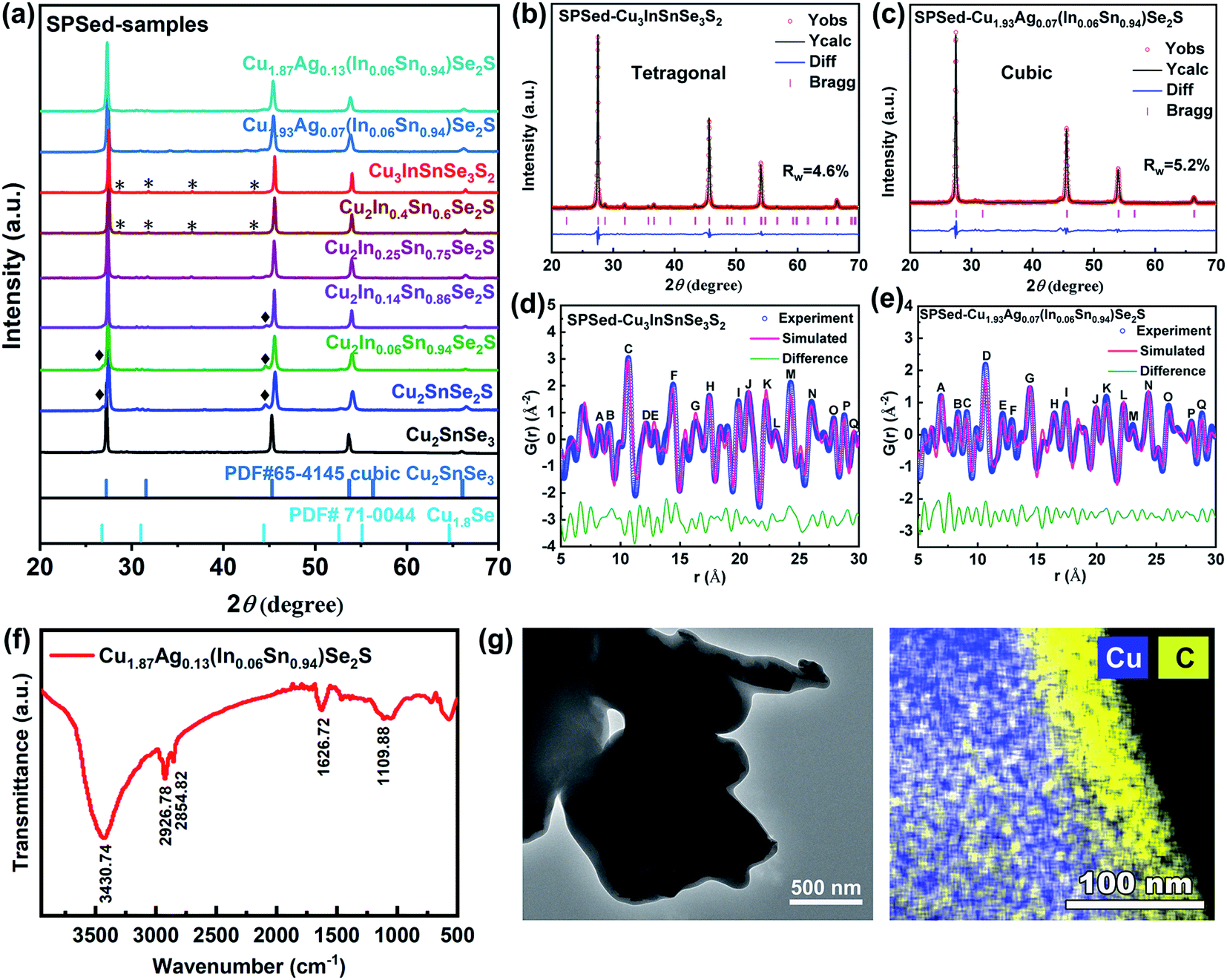 | ||
| Fig. 1 (a) Powder X-ray diffraction (PXRD) patterns of the SPSed-samples. Rietveld refinement results of (b) SPSed-Cu3InSnSe3S2 and (c) SPSed-Cu1.93Ag0.07(In0.06Sn0.94)Se2S. PDF fit to the G(r) function in the range of 5–30 Å using the tetragonal model for (d) SPSed-Cu3InSnSe3S2 and cubic model for (e) SPSed-Cu1.93Ag0.07(In0.06Sn0.94)Se2S. (f) FTIR spectrum of solution-synthesized Cu1.87Ag0.13(In0.06Sn0.94)Se2S. (g) TEM image and EDS element map of Cu and C for SPSed-Cu1.87Ag0.13(In0.06Sn0.94)Se2S. | ||
From a synthetic perspective, a high-entropy system, Cu2−yAgy(InxSn1−x)Se2S (x = 0–0.25, y = 0, 0.07, 0.13), with two metastable phases (wurtzite nanocrystals and cubic nanostructured solids) is obtained, which is hard to realize in their bulk counterparts. Formation energies of the cubic and monoclinic-phase Cu2SnSe3, Cu2SnSe2S, Cu2In0.06Sn0.94Se2S, and Cu1.87Ag0.13(In0.06Sn0.94)Se2S, and tetragonal-phase Cu3InSnSe3S2 are calculated by density functional theory (DFT). Indeed, all monoclinic crystals show lower formation energy than the metastable cubic phase (Table S2†). The colloidal synthetic strategy for monodisperse multinary chalcogenide nanocrystals and the following SPS process are the key factors for the retention of the metastable phase. As shown in Fig. 1f, FTIR spectrometry was performed to verify the surface ligand of OAm in a solution-synthesized Cu1.87Ag0.13(In0.06Sn0.94)Se2S sample. The presence of the OAm molecule is indicated by the symmetric and asymmetric stretching vibrations of –NH2 at 3430.74 cm−1, the bending vibrations of C![[double bond, length as m-dash]](https://www.rsc.org/images/entities/char_e001.gif) C and –NH2 bonds at 1626.72 cm−1, and the bending vibration of the C–N bond at 1109.88 cm−1. During the nanocrystal consolidation process, OAm as a surfactant capping agent at the surface of colloidal nanoparticles can decrease the surface free energy of nanocrystals, simultaneously acting as a controllable molecular solder,45 which might have a dominant effect that restricts the growth of nanoparticles and stabilizes the metastable phase.46–49 Detailed evidence is shown in SEM and TEM images (Fig. 6b andc, and S9a and b†), and the EDS element map of SPSed-Cu1.87Ag0.13(In0.06Sn0.94)Se2S confirms the existence of carbon after sintering (Fig. 1g). In addition, the contents of hydrogen (0.05 wt%) and carbon (1.15 wt%) were measured in the SPSed-Cu1.87Ag0.13(In0.06Sn0.94)Se2S sample, and the results indicate that some of the surface ligands were converted into a mixture of organic hydrocarbons between nanograins of nanostructured solids during the sintering process (Fig. S9c†). Based on size reduction, metastable cubic nanostructured solids Cu2SnSe3 and Cu2−yAgy(InxSn1−x)Se2S (x = 0–0.25, y = 0, 0.07, 0.13) compacted from the corresponding nanoparticles are obtained, which are different from the conventional monoclinic (space group Cc) structure of bulk Cu2SnSe3-based materials.34–36,39–42 In addition, the successful synthesis of Cu2SnSe3 and Cu2SnSe2S cubic nanostructured solids with low configuration entropy provides strong evidence that the metastable cubic phase does not originate from entropy effects, which is different from the strategy for stabilizing the cubic structure by entropy optimization in previous papers.25–27
C and –NH2 bonds at 1626.72 cm−1, and the bending vibration of the C–N bond at 1109.88 cm−1. During the nanocrystal consolidation process, OAm as a surfactant capping agent at the surface of colloidal nanoparticles can decrease the surface free energy of nanocrystals, simultaneously acting as a controllable molecular solder,45 which might have a dominant effect that restricts the growth of nanoparticles and stabilizes the metastable phase.46–49 Detailed evidence is shown in SEM and TEM images (Fig. 6b andc, and S9a and b†), and the EDS element map of SPSed-Cu1.87Ag0.13(In0.06Sn0.94)Se2S confirms the existence of carbon after sintering (Fig. 1g). In addition, the contents of hydrogen (0.05 wt%) and carbon (1.15 wt%) were measured in the SPSed-Cu1.87Ag0.13(In0.06Sn0.94)Se2S sample, and the results indicate that some of the surface ligands were converted into a mixture of organic hydrocarbons between nanograins of nanostructured solids during the sintering process (Fig. S9c†). Based on size reduction, metastable cubic nanostructured solids Cu2SnSe3 and Cu2−yAgy(InxSn1−x)Se2S (x = 0–0.25, y = 0, 0.07, 0.13) compacted from the corresponding nanoparticles are obtained, which are different from the conventional monoclinic (space group Cc) structure of bulk Cu2SnSe3-based materials.34–36,39–42 In addition, the successful synthesis of Cu2SnSe3 and Cu2SnSe2S cubic nanostructured solids with low configuration entropy provides strong evidence that the metastable cubic phase does not originate from entropy effects, which is different from the strategy for stabilizing the cubic structure by entropy optimization in previous papers.25–27
In order to understand the local and long-range structures of the as-obtained nanostructured solids, an X-ray pair distribution function (X-PDF) analysis was performed. The corresponding Rietveld results are shown in Fig. 1d and e, and S1d and e.† It is evident that the global X-PDF structures of simulated structure models provide good descriptions of all the samples, demonstrating the overall crystallographic structure. The peaks with chemical bonding information in the diagrams labeled by letters can be well assigned to the atomic pair distances of the samples (Table S3†). As shown in Fig. 1e and S1e,† the residual curve (green curve) of the cubic model establishes much smoother characteristics in the large range from 10 Å to 30 Å, demonstrating long-range highly crystalline structures. In contrast, the local bonding interactions (5–10 Å) deviate significantly from the simulated profile for the cubic model, as observed from the asymmetric peaks and large fluctuations in the green line. Such a phenomenon is an indication of the local structural distortion with the unbalanced long and short bond lengths. The coexistence of the high-symmetry long-range structure and distorted local structure could be an example of ideal thermoelectric materials based on the ‘phonon-glass, electron-crystal’ concept that could lead to high electrical conductivity and low thermal conductivity and finally achieve a high ZT value.50,51
2.2 Microstructure and composition
The microstructures of the as-synthesized samples were comprehensively characterized. First, the hexagonal (wurtzite) structure of Cu2SnSe3 is confirmed with an average size of around 30 (±10) nm by transmission electron microscopy (TEM) (Fig. S3a and b†). Then, thiol is added to the reaction system as the S source and surfactant capping agent, which can passivate the crystalline facets of the wurtzite nanocrystals, and thus realize size control. As a result, the synthesized Cu2SnSe2S and Cu3InSnSe3S2 nanocrystals show hexagonal structures with an average size of 10 (±2) nm (Fig. S4a and b and S5a†). Elemental mapping measurement was performed to identify the presence of Cu, Ag, In, Sn, Se, and S elements in nanoparticles of Cu2SnSe3, Cu2SnSe2S, SPSed-Cu2SnSe3, SPSed-Cu2SnSe2S, and SPSed-Cu1.87Ag0.13(In0.06Sn0.94)Se2S. All elements in the samples show homogeneous distributions, and no significant local element enrichment is observed (Fig. S3c, S4c, S6b, S7b and S11d†). For nanostructured solids, Fig. S9a and b† show the scanning electron microscopy (SEM) surface micrographs of SPSed-Cu2In0.06Sn0.94Se2S and SPSed-Cu1.87Ag0.13(In0.06Sn0.94)Se2S pellets. A slight grain growth of nanoparticles can be observed during the sintering process and the final average grain sizes are 63.06 (±30) and 131.98 (±50) nm for SPSed-Cu2In0.06Sn0.94Se2S and SPSed-Cu1.87Ag0.13(In0.06Sn0.94)Se2S, respectively. Fig. S10a and d and S11a† show the high-resolution TEM (HRTEM) images of the SPSed-Cu2SnSe3, SPSed-Cu2SnSe2S, and SPSed-Cu1.87Ag0.13(In0.06Sn0.94)Se2S samples. The inverse fast Fourier transform (IFFT) images (Fig. S10b and e and S11b†) clearly show the highly dense dislocation arrays. In order to investigate the strain fields from distorted lattices caused by the strong mismatch of the atomic radius, geometric phase analysis (GPA) was performed based on IFFT images to calculate the strains. As shown in Fig. S10c and f and S11c,† strong strain distribution fluctuations can be observed in the SPSed samples, which should strongly affect the thermal transport process.To further verify the single-phase and high-entropy configuration in the as-synthesized Cu3InSnSe3S2 and SPSed-Cu3InSnSe3S2, high-angle annular dark-field scanning transmission electron microscopy (HAADF-STEM) was conducted. Fig. 2a and e show the HAADF-STEM images of a Cu3InSnSe3S2 nanoparticle and SPSed-Cu3InSnSe3S2 nanostructured solid viewed along the [001] and [110] zone axes, respectively. The atomic models of the hexagonal structure and tetragonal structure are in good agreement with the experimental images, indicating the consistency of the atomic lattices and positions of all atoms (Fig. 2b and f). As shown in Fig. 2d, all elements are distributed in the nanoparticle, and Cu and S are a little bit aggregated in the center of the particle. From our results and some literature reports,52,53 we believe that the copper thiolate in solution could preferentially decompose into a Cu2−xS crystal nucleus due to its higher reactively. Then highly active diphenyl diselenide (PhSeSePh) rapidly decomposes at high temperatures after injection and triggers the growth of nanocrystals, in which Se, Sn and In atoms gradually diffuse into the Cu2−xS crystal nucleus simultaneously with the epitaxial growth and maturation process. Therefore, enrichment of Cu and S elements in the middle of individual nanoparticles can be attributed to the preferential nucleation process of 1-dodecanethiol (both as a ligand and sulfur source) in the precursor solution and Cu before the injection of Se sources. As shown in Fig. 2h and S8,† the EDS mapping of the SPSed-Cu3InSnSe3S2 sample demonstrates that the distribution of all elements is homogeneous in the nanostructured solid.
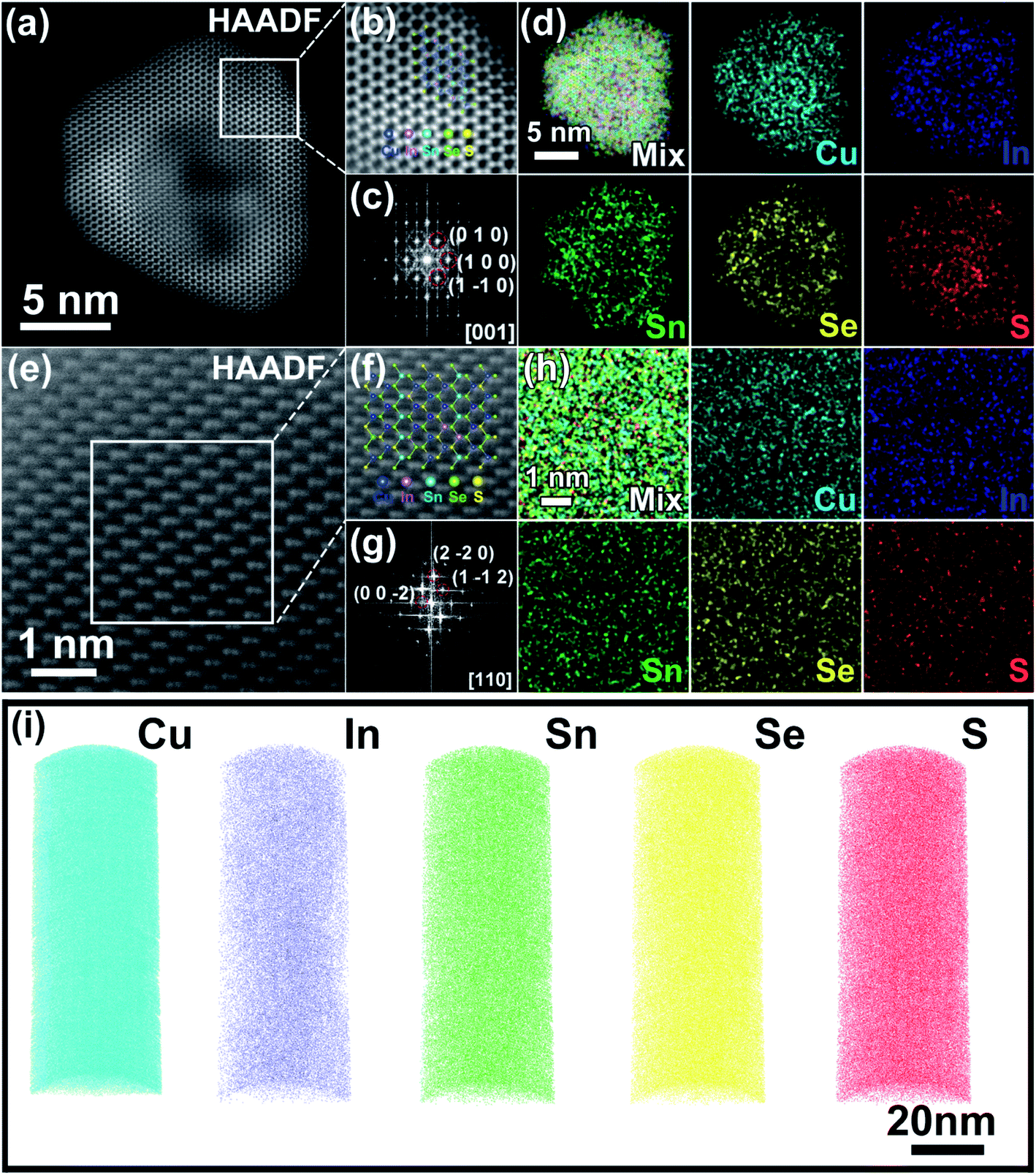 | ||
| Fig. 2 Atomic structure recognition of solution-synthesized and SPSed-Cu3InSnSe3S2. (a) Atomic-resolution HAADF-STEM image, (b) atomic model, (c) corresponding FFT along the [001] zone axis and (d) EDS mapping of the as-synthesized Cu3InSnSe3S2 nanoparticle. (e) Atomic-resolution HAADF-STEM image, (f) atomic model, (g) corresponding FFT along the [110] zone axis and (h) EDS mapping of the SPSed-Cu3InSnSe3S2 sample. (i) 3D-APT images showing the elemental distribution and multicomponent nature in the SPSed-Cu2In0.09Sn0.91Se2S. | ||
Atom probe tomography (APT) analysis provides the mapping of three-dimensional microstructural and compositional information with sub-nanometer spatial accuracy and elemental sensitivity in the range of tens of ppm,54 which can provide solid evidence that these elements are indeed homogeneously distributed in the nanostructured solid at the atomic scale. The 3D atomic maps and the nearest-neighbor (NN) atomic distribution of SPSed-Cu2In0.09Sn0.91Se2S are shown in Fig. 2i and S14,† respectively. The measured NN atomic distance histograms of each element completely overlap with the calculated curves (Fig. S14†) without deviating from the randomized Gaussian peak, revealing the homogeneous distribution of the Cu, In, Sn, Se, and S elements. The homogeneous and disordered distribution of all the elements on the macroscale, nanoscale, and atomic-scale confirms that the as-synthesized nanostructured solid is a high-entropy multinary metal chalcogenide.
2.3 Electronic and phononic band structures
To gain insight into the evolution of electronic states in the conventional monoclinic structure and metastable cubic structure, DFT calculations were performed. Fig. 3a and b show the electronic band structures of monoclinic and cubic Cu1.87Ag0.13(In0.06Sn0.94)Se2S, respectively. Those of Cu2SnSe3, Cu2SnSe2S, and Cu2In0.06Sn0.94Se2S are shown in Fig. S15.† The monoclinic and cubic Cu2SnSe3 are direct-band-gap semiconductors with band gaps (Eg) of 0.12 and 0.11 eV, respectively (Fig. S15a and b†). Eg can be effectively enlarged by alloying S into the anionic site of Cu2SnSe3 (Fig. S15c and d†). In-Doped Cu2SnSe2S pushes the Fermi level (Ef) deep into the multiple bands and turns Cu2In0.06Sn0.94Se2S into a highly degenerate semiconductor (Fig. S15e and f†), which thus increases channels for electrical transport. From the valence bands near the Fermi level that are highlighted by the red circles in Fig. 3a and b and S15,† we find that the top three valence bands at the Γ point of the monoclinic structure display band splitting while the cubic structure is degenerate. The cubic phase with high degeneracy can lead to more energy valleys participating in electrical transport.13 | ||
| Fig. 3 The electronic energy band structures for (a) monoclinic Cu1.87Ag0.13(In0.06Sn0.94)Se2S and (b) cubic Cu1.87Ag0.13(In0.06Sn0.94)Se2S. The phonon dispersions of (c) monoclinic Cu2SnSe3 and (d) cubic Cu2SnSe3. | ||
To gain insight into phonon and thermal properties, we calculated the phonon dispersion relations of monoclinic and cubic Cu2SnSe3 based on DFT, as shown in Fig. 3c and d. The monoclinic phase has 12 atoms in a primitive cell and thus 36 phonon branches (Fig. S16a†). The cubic phase has a zinc blende structure, in which Cu and Sn randomly occupy the cation sites with a ratio of 2![[thin space (1/6-em)]](https://www.rsc.org/images/entities/char_2009.gif) :1, and Se occupies the anion sites (Fig. S16b†). We used the virtual crystal approximation (VCA) to calculate the phonon dispersion of the cubic phase. Under VCA, the cubic phase has a primitive cell that consists of 2 atoms – a virtual atom, made of 2/3 Cu and 1/3 Sn, and a Se atom. The phonon dispersion of the cubic phase does not show any imaginary frequency, indicating that the structure is locally stable. The maximum frequency of the cubic phase is larger than that of the monoclinic phase, indicating that the cubic phase may have stronger bonds. The phonon group velocity, especially for the longitudinal acoustic (LA) branch, of the cubic phase is much larger than that of the monoclinic phase (Fig. S16c†). The volumetric heat capacity of the cubic phase is slightly larger than that of the monoclinic phase (Fig. S16d†), partially because the cubic phase has higher symmetry and packing density. Based on phonon kinetic theory, the lattice thermal conductivity is kL = 1/3cv2τ, in which c is the heat capacity, v is the group velocity, and τ is the phonon relaxation time. Since the cubic phase has larger c and v than the monoclinic phase, its τ must be much smaller, in order to have similar or lower kL. This inference indicates that the disorder and distortion induced by Cu/Sn alloying that was not considered in the VCA in the cubic phase must be strong and induce severe phonon scattering. Additionally, grain boundaries, dislocations, Ag and S alloying and In doping further reduce the phonon relaxation time.
:1, and Se occupies the anion sites (Fig. S16b†). We used the virtual crystal approximation (VCA) to calculate the phonon dispersion of the cubic phase. Under VCA, the cubic phase has a primitive cell that consists of 2 atoms – a virtual atom, made of 2/3 Cu and 1/3 Sn, and a Se atom. The phonon dispersion of the cubic phase does not show any imaginary frequency, indicating that the structure is locally stable. The maximum frequency of the cubic phase is larger than that of the monoclinic phase, indicating that the cubic phase may have stronger bonds. The phonon group velocity, especially for the longitudinal acoustic (LA) branch, of the cubic phase is much larger than that of the monoclinic phase (Fig. S16c†). The volumetric heat capacity of the cubic phase is slightly larger than that of the monoclinic phase (Fig. S16d†), partially because the cubic phase has higher symmetry and packing density. Based on phonon kinetic theory, the lattice thermal conductivity is kL = 1/3cv2τ, in which c is the heat capacity, v is the group velocity, and τ is the phonon relaxation time. Since the cubic phase has larger c and v than the monoclinic phase, its τ must be much smaller, in order to have similar or lower kL. This inference indicates that the disorder and distortion induced by Cu/Sn alloying that was not considered in the VCA in the cubic phase must be strong and induce severe phonon scattering. Additionally, grain boundaries, dislocations, Ag and S alloying and In doping further reduce the phonon relaxation time.
2.4 Thermoelectric properties
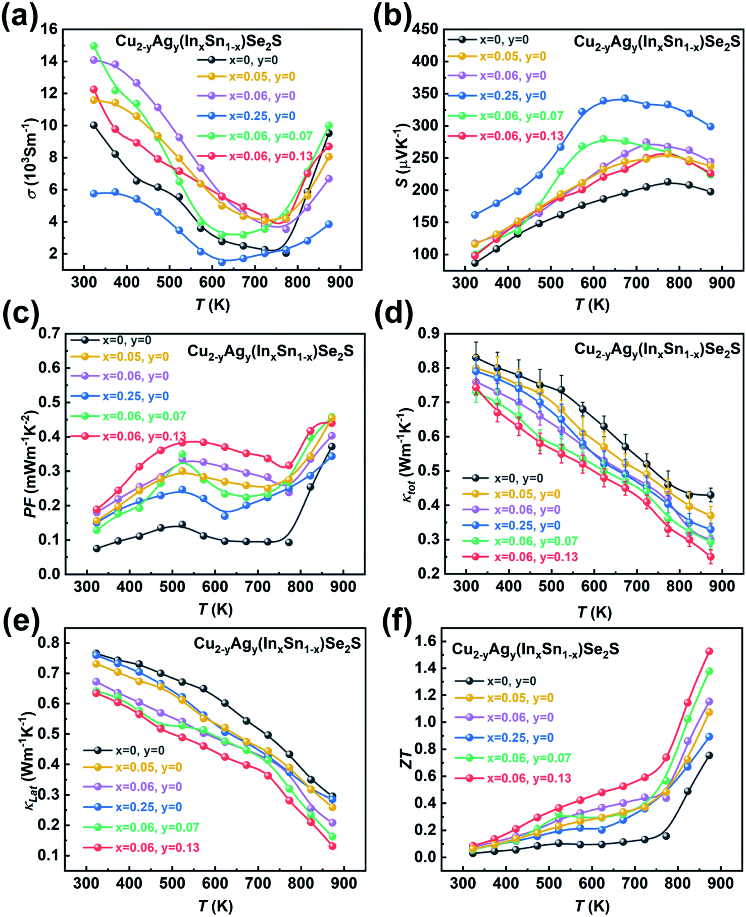 | ||
| Fig. 4 Temperature dependence of (a) electrical conductivity σ, (b) Seebeck coefficient S, (c) power factor PF, (d) total thermal conductivity ktot, (e) lattice thermal conductivity klat and (f) ZT values for Cu2−yAgy(InxSn1−x)Se2S (x = 0, 0.05, 0.06, 0.25, y = 0, 0.07, 0.13). | ||
 | ||
| Fig. 5 (a) Variation of Seebeck coefficient S with carrier concentration p for cubic Cu2In0.06Sn0.94Se2S, in which the blue dotted line is the Pisarenko curve obtained via the SPB model. The previously reported data by Ming et al.35 (monoclinic Cu2Sn1−yInySe2.7S0.3, y = 0–0.21) and Li et al.34 (monoclinic Cu2−xAgxSn1−yInySe3, x = 0–0.15, y = 0–0.15) are depicted by orange triangles and purple half-filled circles, respectively. (b) Schematic illustration of the effect of multiscale defects on phonons, including grain boundaries, point defects, lattice distortion, secondary phase, dislocations and amorphous carbon. Comparison of the reported (c) thermal conductivity and (d) ZT values of Cu2SnSe3-based materials.34–36,39 | ||
The ultralow klat of the as-synthesized samples can be attributed to the following three reasons. First, the intrinsic crystal structure of Cu2SnSe3-based materials leads to low phonon thermal conductivity. More specifically, the Cu–Se bond constructs a conductive framework for controlling hole transport, and cationic doping is allowed to adjust the carrier concentration.58 Such structural characteristics are similar to those of phonon glass electron crystal (PGEC) compounds,50,51 which can be confirmed by low-temperature Cp measurement (Fig. S22†). The plot of Cpvs. T can be fitted by a Debye model combined with three Einstein modes (black line, the detailed calculation is shown in the ESI†), which illustrates that the contribution to Cp at low temperature is dominated by low-energy optical modes resulting from the weakly bound Cu or Ag-rattlers (Einstein oscillators) that suppress lattice thermal conductivity (klat).59–61 Second, the configurational entropy in a material increases through doping and alloying (Fig. S23†). Based on the Boltzmann hypothesis, the configurational entropy (ΔS) is given by:27
 | (1) |
Fig. 4f shows the temperature dependence of ZT values for Cu2−yAgy(InxSn1−x)Se2S. Owing to the high PF and low thermal conductivity, Cu1.87Ag0.13(In0.06Sn0.94)Se2S shows the maximum ZT of 1.52 at 873 K. Compared to the ZT values reported in Cu2SnSe3-based systems in the literature,34–36,39 our value is essentially record-high, as shown in Fig. 5d. Compared with the klat and carrier mobility (μH) at ∼300 K in the monoclinic-phase Cu2Sn0.82In0.18Se2.7S0.3 and Cu1.85Ag0.15Sn0.9In0.1Se3 reported by Ming et al.35 and Li et al.,34 a relatively low klat and μH (Table S5†) are obtained in our cubic Cu2In0.06Sn0.94Se2S sample due to the nano-grain size, which enhances the grain boundary scattering for the charge carrier. The ultralow klat can compensate for the deterioration in electrical conductivity, which can be understood from the quality factor,65β = (μH/klat)(md*/me)3/2 (Table S5†), taking into account the klat and μH in the numerator and denominator, respectively.
The reproducibility of thermoelectric performance for Cu1.87Ag0.13(In0.06Sn0.94)Se2S is provided in Fig. S24.† Besides, the thermal stability is a critical concern for metastable phases in the thermoelectric community. Thus, the XRD patterns of SPSed-Cu2In0.05Sn0.95Se2S before testing and after the 3rd electrical test were measured, and no change in phase structure is found (Fig. 6a). Additionally, after measuring the electrical properties three times, the SPSed-Cu2In0.05Sn0.95Se2S sample could still maintain the same grain size (Fig. 6b and c). The electrical performance was re-measured three times for Cu2In0.05Sn0.95Se2S and shows no deterioration (Fig. 6d–f).
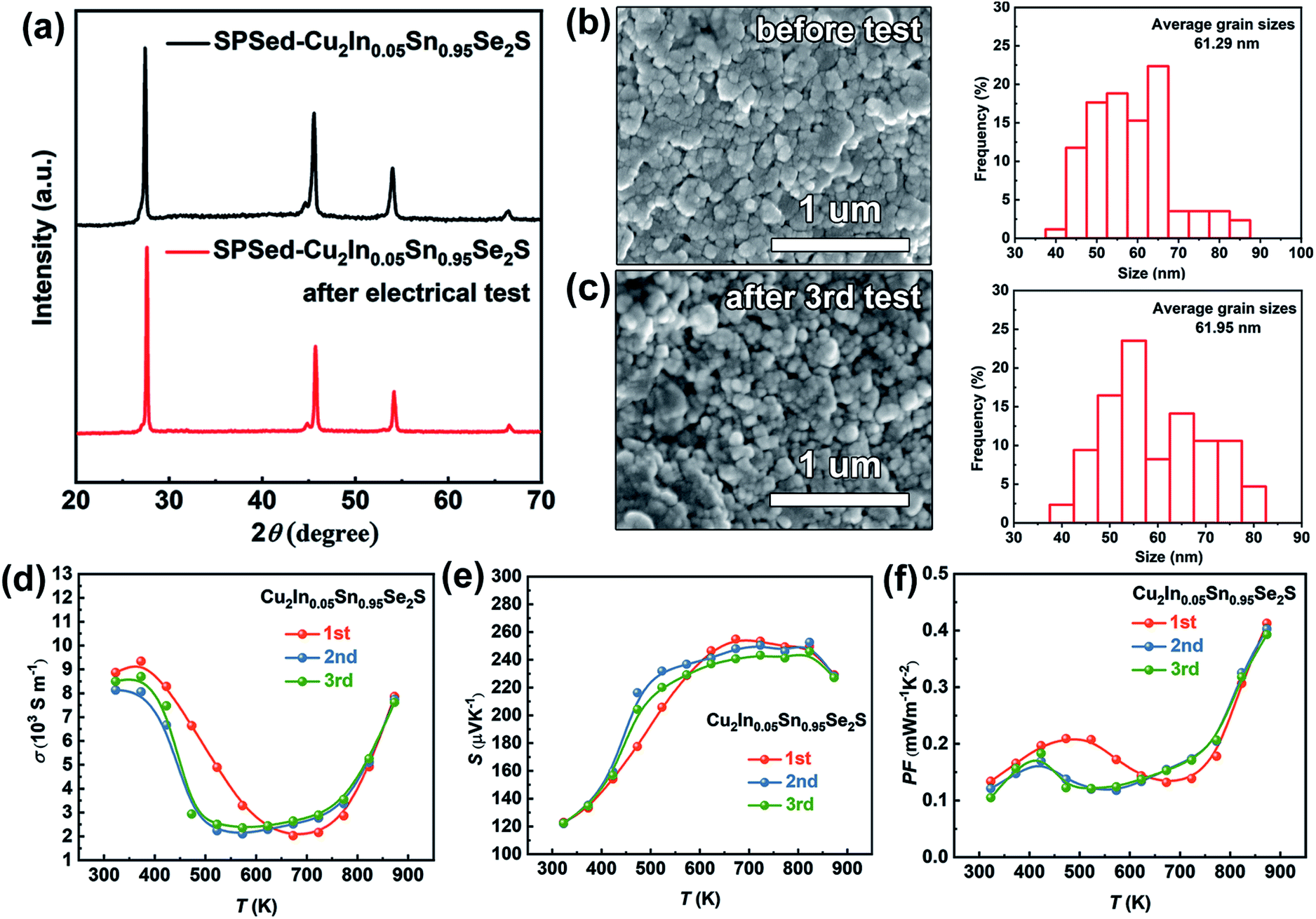 | ||
| Fig. 6 The thermal stability tests for Cu2In0.05Sn0.95Se2S. (a) XRD patterns before testing and after the 3rd electrical test. (b and c) SEM micrographs of sintered pellets before testing and after three rounds of electrical tests. (d–f) Cyclic tests of electrical conductivity σ, Seebeck coefficient S and power factor PF. | ||
3. Conclusions
In summary, we have successfully synthesized a high-entropy system, Cu2−yAgy(InxSn1−x)Se2S (x = 0–0.25, y = 0, 0.07, 0.13), by adopting a hot-injection strategy and characterized the thermoelectric properties of dense materials compacted from those nanoparticles. We propose a new synthetic route for compacting nanocrystals without eliminating long organic ligands and subsequently obtain a series of high-entropy multinary chalcogenide nanocrystals with a metastable cubic phase induced by size-driven structural stabilization. Through phase and entropy design, a high power factor (0.44 mW m−1 K−2) and an ultralow thermal conductivity (0.25 W m−1 K−1) are achieved at 873 K for the Cu1.87Ag0.13(In0.06Sn0.94)Se2S sample. A high ZT of 1.52 is achieved which is about 204% higher than that of pristine Cu2SnSe3. This work provides a new strategy for stabilizing the metastable phase through ligand retention induced small size and may have broader application in various fields such as photocatalysis, electronic devices, and photovoltaics.Data availability
Chemicals, preparation of Cu2SnSe3, Cu2SnSe2S, Cu2InxSn1−xSe2S, Cu3InSnSe3S2 and Cu2−yAgy(In0.06Sn0.94)Se2S nanocrystals, spark plasma sintering, characterization, measurement of thermoelectric properties, DFT calculation, formation energy calculation, the calculation details of Lorentz factor (L) and density of states effective mass (m*d) via single parabolic band (SPB) model, the calculation details of heat capacity Cpvia the Debye-3 Einstein model, crystal structure characterization, microstructure and composition, electronic and phononic band structures and thermoelectric properties are available in the ESI.†Author contributions
Wanjia Zhang: investigation, methodology, data curation, formal analysis, visualization, writing – original draft. Yue Lou: resources, supervision, writing – review & editing. Hongliang Dong: synchrotron X-ray diffraction testing. Fanshi Wu: formal analysis, DFT calculation, writing – original draft. Janak Tiwari: formal analysis, DFT calculation, writing – original draft. Zhan Shi: resources, writing – reviewing. Sokrates T. Pantelides: supervision, writing – reviewing. Tianli Feng: conceptualization, DFT calculation, writing – review & editing, supervision. Biao Xu: conceptualization, writing – review & editing, supervision, project administration, funding acquisition.Conflicts of interest
The authors declare no competing financial interest.Acknowledgements
B. X. is thankful for financial support from Jiangsu Specially Appointed Professorship, the Jiangsu Provincial Innovation and Entrepreneurship Doctor Program, and the 1000 Young Talents Program. Y. L. is thankful for financial support from the Jiangsu Provincial Innovation and Entrepreneurship Doctor Program (JSSCBS20210215). The support and resources from the Center for High-Performance Computing at the University of Utah and the National Energy Research Scientific Computing Center (NERSC) are gratefully acknowledged. We thank the staff of the BL17B1 beamline of the National Facility for Protein Science in Shanghai (NFPS) at the Shanghai Synchrotron Radiation Facility.References
- B. Hu, X.-L. Shi, J. Zou and Z.-G. Chen, Chem. Eng. J., 2022, 437, 135268 CrossRef CAS.
- L. Li, W. D. Liu, Q. Liu and Z. G. Chen, Adv. Funct. Mater., 2022, 32, 2200548 CrossRef CAS.
- Z.-G. Chen and W.-D. Liu, J. Mater. Sci. Technol., 2022, 121, 256–262 CrossRef.
- W.-Y. Chen, X.-L. Shi, J. Zou and Z.-G. Chen, Small Methods, 2022, 6, 2101235 CrossRef PubMed.
- M. Li, M. Hong, M. Dargusch, J. Zou and Z.-G. Chen, Trends Chem., 2021, 3, 561–574 CrossRef CAS.
- Z.-Z. Luo, S. Cai, S. Hao, T. P. Bailey, I. Spanopoulos, Y. Luo, J. Xu, C. Uher, C. Wolverton, V. P. Dravid, Q. Yan and M. G. Kanatzidis, Angew. Chem., Int. Ed., 2021, 60, 268–273 CrossRef CAS PubMed.
- Q. Liu, Z. Zhao, Y. Lin, P. Guo, S. Li, D. Pan and X. Ji, Chem. Commun., 2011, 47, 964–966 RSC.
- D. Sarkar, T. Ghosh, A. Banik, S. Roychowdhury, D. Sanyal and K. Biswas, Angew. Chem., Int. Ed., 2020, 59, 11115–11122 CrossRef CAS PubMed.
- Y. Pei, X. Shi, A. LaLonde, H. Wang, L. Chen and G. J. Snyder, Nature, 2011, 473, 66–69 CrossRef CAS PubMed.
- J. P. Heremans, B. Wiendlocha and A. M. Chamoire, Energy Environ. Sci., 2012, 5, 5510–5530 RSC.
- J. P. Heremans, V. Jovovic, E. S. Toberer, A. Saramat, K. Kurosaki, A. Charoenphakdee, S. Yamanaka and G. J. Snyder, Science, 2008, 321, 554–557 CrossRef CAS PubMed.
- L. Hu, T. Zhu, X. Liu and X. Zhao, Adv. Funct. Mater., 2014, 24, 5211–5218 CrossRef CAS.
- L. Hu, Y. Luo, Y.-W. Fang, F. Qin, X. Cao, H. Xie, J. Liu, J. Dong, A. Sanson, M. Giarola, X. Tan, Y. Zheng, A. Suwardi, Y. Huang, K. Hippalgaonkar, J. He, W. Zhang, J. Xu, Q. Yan and M. G. Kanatzidis, Adv. Energy Mater., 2021, 11, 2100661 CrossRef CAS.
- Y. Kinemuchi, M. Mikami, K. Kobayashi, K. Watari and Y. Hotta, J. Electron. Mater., 2010, 39, 2059–2063 CrossRef CAS.
- K. Peng, H. Wu, Y. Yan, L. Guo, G. Wang, X. Lu and X. Zhou, J. Mater. Chem. A, 2017, 5, 14053–14060 RSC.
- X.-L. Shi, W.-D. Liu, M. Li, Q. Sun, S.-D. Xu, D. Du, J. Zou and Z.-G. Chen, Adv. Energy Mater., 2022, 12, 2200670 CrossRef CAS.
- M. Li, Q. Sun, S.-D. Xu, M. Hong, W.-Y. Lyu, J.-X. Liu, Y. Wang, M. Dargusch, J. Zou and Z.-G. Chen, Adv. Mater., 2021, 33, 2102575 CrossRef CAS PubMed.
- W.-D. Liu, Y. Yu, M. Dargusch, Q. Liu and Z.-G. Chen, Renewable Sustainable Energy Rev., 2021, 141, 110800 CrossRef CAS.
- W.-D. Liu, L. Yang and Z.-G. Chen, Nano Today, 2020, 35, 100938 CrossRef CAS.
- Y. Sun, C.-A. Di, W. Xu and D. Zhu, Adv. Electron. Mater., 2019, 5, 1800825 CrossRef CAS.
- B. Bai, M. Xu, N. Li, W. Chen, J. Liu, J. Liu, H. Rong, D. Fenske and J. Zhang, Angew. Chem., Int. Ed., 2019, 58, 4852–4857 CrossRef CAS PubMed.
- H. F. Cheng, N. L. Yang, Q. P. Lu, Z. C. Zhang and H. Zhang, Adv. Mater., 2018, 30, 1707189 CrossRef PubMed.
- J. Liu, J. Huang, W. Niu, C. Tan and H. Zhang, Chem. Rev., 2021, 121, 5830–5888 CrossRef CAS PubMed.
- Y. Chen, Z. Lai, X. Zhang, Z. Fan, Q. He, C. Tan and H. Zhang, Nat. Rev. Chem., 2020, 4, 243–256 CrossRef CAS.
- Y. Luo, T. Xu, Z. Ma, D. Zhang, Z. Guo, Q. Jiang, J. Yang, Q. Yan and M. G. Kanatzidis, J. Am. Chem. Soc., 2021, 143, 13990–13998 CrossRef CAS PubMed.
- S. Roychowdhury, T. Ghosh, R. Arora, U. V. Waghmare and K. Biswas, Angew. Chem., Int. Ed., 2018, 57, 15167–15171 CrossRef CAS PubMed.
- H. Zhu, T. Zhao, B. Zhang, Z. An, S. Mao, G. Wang, X. Han, X. Lu, J. Zhang and X. Zhou, Adv. Energy Mater., 2021, 11, 2003304 CrossRef CAS.
- L. Hu, Y. Zhang, H. Wu, J. Li, Y. Li, M. Mckenna, J. He, F. Liu, S. J. Pennycook and X. Zeng, Adv. Energy Mater., 2018, 8, 1802116 CrossRef.
- B. Jiang, Y. Yu, J. Cui, X. Liu, L. Xie, J. Liao, Q. Zhang, Y. Huang, S. Ning, B. Jia, B. Zhu, S. Bai, L. Chen, S. J. Pennycook and J. He, Science, 2021, 371, 830–834 CrossRef CAS PubMed.
- Y. Luo, S. Hao, S. Cai, T. J. Slade, Z. Z. Luo, V. P. Dravid, C. Wolverton, Q. Yan and M. G. Kanatzidis, J. Am. Chem. Soc., 2020, 142, 15187–15198 CrossRef CAS PubMed.
- H. Duan, Z. Cheng, Y. Xue, Z. Cui, M. Yang and S. Wang, J. Electroanal. Chem., 2021, 882, 115037 CrossRef CAS.
- M. Wang, Z. Cui, Y. Xue, A. Yan, X. Yu, X. Song and H. Li, Electroanalysis, 2019, 31, 1316–1323 CrossRef CAS.
- C. Wang, Z. Cui, Y. Xue, Y. Wang, M. Wang, B. Ji, J. Chen, Y. Xue and L. Zhang, Thermochim. Acta, 2022, 708, 179140 CrossRef CAS.
- Y. Li, G. Liu, T. Cao, L. Liu, J. Li, K. Chen, L. Li, Y. Han and M. Zhou, Adv. Funct. Mater., 2016, 26, 6025–6032 CrossRef CAS.
- H. Ming, G. Zhu, C. Zhu, X. Qin, T. Chen, J. Zhang, D. Li, H. Xin and B. Jabar, ACS Nano, 2021, 15, 10532–10541 CrossRef PubMed.
- H. Ming, C. Zhu, X. Qin, J. Zhang, D. Li, B. Zhang, T. Chen, J. Li, X. Lou and H. Xin, ACS Appl. Mater. Interfaces, 2020, 12, 19693–19700 CrossRef CAS PubMed.
- E. J. Skoug, J. D. Cain and D. T. Morelli, J. Alloys Compd., 2010, 506, 18–21 CrossRef CAS.
- R. Ma, G. Liu, Y. Li, J. Li, K. Chen, Y. Han, M. Zhou and L. Li, J. Asian Ceram. Soc., 2018, 6, 13–19 CrossRef.
- X. Cheng, Z. Li, Y. You, T. Zhu, Y. Yan, X. Su and X. Tang, ACS Appl. Mater. Interfaces, 2019, 11, 24212–24220 CrossRef CAS PubMed.
- Y. Zhou, H. Wu, D. Wang, L. Fu, Y. Zhang, J. He, S. J. Pennycook and L. D. Zhao, Mater. Today Phys., 2018, 7, 77–88 CrossRef.
- G. Marcano, C. Rincón, S. A. López, G. Sánchez Pérez, J. L. Herrera-Pérez, J. G. Mendoza-Alvarez and P. Rodríguez, Solid State Commun., 2011, 151, 84–86 CrossRef CAS.
- H. Ming, C. Zhu, X. Qin, B. Jabar, T. Chen, J. Zhang, H. Xin, D. Li and J. Zhang, Nanoscale, 2021, 13, 4233–4240 RSC.
- Y. Lou, W. Zhao, C. Li, H. Huang, T. Bai, C. Chen, C. Liang, Z. Shi, D. Zhang, X.-B. Chen and S. Feng, ACS Appl. Mater. Interfaces, 2017, 9, 18046–18053 CrossRef CAS PubMed.
- Y. Liu, M. Calcabrini, Y. Yu, S. Lee, C. Chang, J. David, T. Ghosh, M. C. Spadaro, C. Xie, O. Cojocaru-Mirédin, J. Arbiol and M. Ibáñez, ACS Nano, 2022, 16, 78–88 CrossRef CAS PubMed.
- F.-J. Fan, L. Wu and S.-H. Yu, Energy Environ. Sci., 2014, 7, 190–208 RSC.
- X. Wang, X. Liu, D. Yin, Y. Ke and M. T. Swihart, Chem. Mater., 2015, 27, 3378–3388 CrossRef CAS.
- W. W. Yu, Y. A. Wang and X. Peng, Chem. Mater., 2003, 15, 4300–4308 CrossRef CAS.
- M. E. Norako, M. J. Greaney and R. L. Brutchey, J. Am. Chem. Soc., 2012, 134, 23–26 CrossRef CAS PubMed.
- J. Jeong, H. Chung, Y. C. Ju, J. Moon, J. Roh, S. Yoon, Y. R. Do and W. Kim, Mater. Lett., 2010, 64, 2043–2045 CrossRef CAS.
- M. Beekman, D. T. Morelli and G. S. Nolas, Nat. Mater., 2015, 14, 1182–1185 CrossRef CAS PubMed.
- CRC Handbook of Thermoelectrics, ed. G. A. Slack and D. M. Rowe, CRC Press, Boca Raton, FL, USA, 1995 Search PubMed.
- M. B. Sigman, A. Ghezelbash, T. Hanrath, A. E. Saunders, F. Lee and B. A. Korgel, J. Am. Chem. Soc., 2003, 125, 16050–16057 CrossRef CAS PubMed.
- W. P. Lim, C. T. Wong, S. L. Ang, H. Y. Low and W. S. Chin, Chem. Mater., 2006, 18, 6170–6177 CrossRef CAS.
- Y. Yu, C. Zhou, S. Zhang, M. Zhu, M. Wuttig, C. Scheu, D. Raabe, G. J. Snyder, B. Gault and O. Cojocaru-Mirédin, Mater. Today, 2020, 32, 260–274 CrossRef CAS.
- S. Roychowdhury, T. Ghosh, R. Arora, M. Samanta, L. Xie, N. K. Singh, A. Soni, J. He, U. V. Waghmare and K. Biswas, Science, 2021, 371, 722–727 CrossRef CAS PubMed.
- Q. D. Gibson, T. Zhao, L. M. Daniels, H. C. Walker, R. Daou, S. Hébert, M. Zanella, M. S. Dyer, J. B. Claridge, B. Slater, M. W. Gaultois, F. Corà, J. Alaria and M. J. Rosseinsky, Science, 2021, 373, 1017–1022 CrossRef CAS PubMed.
- W. Lin, J. He, X. Su, X. Zhang, Y. Xia, T. P. Bailey, C. C. Stoumpos, G. Tan, A. J. E. Rettie, D. Y. Chung, V. P. Dravid, C. Uher, C. Wolverton and M. G. Kanatzidis, Adv. Mater., 2021, 33, 2104908 CrossRef CAS PubMed.
- X. Shi, L. Xi, J. Fan, W. Zhang and L. Chen, Chem. Mater., 2010, 22, 6029–6031 CrossRef CAS.
- M. K. Jana, K. Pal, A. Warankar, P. Mandal, U. V. Waghmare and K. Biswas, J. Am. Chem. Soc., 2017, 139, 4350–4353 CrossRef CAS PubMed.
- J. L. Baker, J. T. White, A. Chen, T. Ulrich, R. R. Roback and H. Xu, J. Nucl. Mater., 2021, 557, 153282 CrossRef CAS.
- B. Koley, A. Lakshan, P. R. Raghuvanshi, C. Singh, A. Bhattacharya and P. P. Jana, Angew. Chem., Int. Ed., 2021, 60, 9106–9113 CrossRef CAS PubMed.
- R. Liu, H. Chen, K. Zhao, Y. Qin, B. Jiang, T. Zhang, G. Sha, X. Shi, C. Uher, W. Zhang and L. Chen, Adv. Mater., 2017, 29, 1702712 CrossRef PubMed.
- G. Yang, L. Sang, F. F. Yun, D. R. G. Mitchell, G. Casillas, N. Ye, K. See, J. Pei, X. Wang, J.-F. Li, G. J. Snyder and X. Wang, Adv. Funct. Mater., 2021, 31, 2008851 CrossRef CAS.
- M. Li, D. L. Cortie, J. Liu, D. Yu, S. M. K. N. Islam, L. Zhao, D. R. G. Mitchell, R. A. Mole, M. B. Cortie, S. Dou and X. Wang, Nano Energy, 2018, 53, 993–1002 CrossRef CAS.
- L.-P. Hu, T.-J. Zhu, Y.-G. Wang, H.-H. Xie, Z.-J. Xu and X.-B. Zhao, NPG Asia Mater., 2014, 6, e88 CrossRef CAS.
Footnotes |
| † Electronic supplementary information (ESI) available: List of chemicals, preparation of Cu2SnSe3, Cu2SnSe2S, Cu2InxSn1−xSe2S, Cu3InSnSe3S2 and Cu2−yAgy(In0.06Sn0.94)Se2S nanocrystals, spark plasma sintering, characterization, measurement of thermoelectric properties, DFT calculation, formation energy calculation, the calculation details of the Lorentz factor (L) and density of states effective mass (md*) via the single parabolic band (SPB) model, the calculation details of heat capacity Cpvia the Debye-3 Einstein model, crystal structure characterization, microstructure and composition, electronic and phononic band structures and thermoelectric properties. See https://doi.org/10.1039/d2sc02915d |
| ‡ These two authors contributed equally. |
| This journal is © The Royal Society of Chemistry 2022 |