
 Open Access Article
 This Open Access Article is licensed under a
 Creative Commons Attribution 3.0 Unported Licence
Atomic and structural modifications of two-dimensional transition metal dichalcogenides for various advanced applications
Balakrishnan
Kirubasankar†
 ab,
Yo Seob
Won†
ac,
Laud Anim
Adofo†
ac,
Soo Ho
Choi
c,
Soo Min
Kim
*b and
Ki Kang
Kim
*ac
ab,
Yo Seob
Won†
ac,
Laud Anim
Adofo†
ac,
Soo Ho
Choi
c,
Soo Min
Kim
*b and
Ki Kang
Kim
*ac
aDepartment of Energy Science, Sungkyunkwan University, Suwon 16419, South Korea. E-mail: kikangkim@skku.edu
bDepartment of Chemistry, Sookmyung Women's University, Seoul 14072, South Korea. E-mail: soominkim@sookmyung.ac.kr
cCenter for Integrated Nanostructure Physics (CINAP), Institute for Basic Science (IBS), Sungkyunkwan University, Suwon 16419, South Korea
First published on 18th May 2022
Abstract
Two-dimensional (2D) transition metal dichalcogenides (TMDs) and their heterostructures have attracted significant interest in both academia and industry because of their unusual physical and chemical properties. They offer numerous applications, such as electronic, optoelectronic, and spintronic devices, in addition to energy storage and conversion. Atomic and structural modifications of van der Waals layered materials are required to achieve unique and versatile properties for advanced applications. This review presents a discussion on the atomic-scale and structural modifications of 2D TMDs and their heterostructures via post-treatment. Atomic-scale modifications such as vacancy generation, substitutional doping, functionalization and repair of 2D TMDs and structural modifications including phase transitions and construction of heterostructures are discussed. Such modifications on the physical and chemical properties of 2D TMDs enable the development of various advanced applications including electronic and optoelectronic devices, sensing, catalysis, nanogenerators, and memory and neuromorphic devices. Finally, the challenges and prospects of various post-treatment techniques and related future advanced applications are addressed.
1. Introduction
Since the discovery of monolayer graphene (Gr) in 2004,1 two-dimensional (2D) transition metal dichalcogenides (TMDs) and their heterostructures have gained significant attention owing to their numerous unique physical and chemical properties, such as high electron mobility,2 thermal conductivity,3 topological insulation,4 Moiré superlattices,5 unconventional superconductivity,6,7 piezoelectricity,8,9 giant magnetoresistance,10 non-linear optics,11–13 and Weyl semimetals.14,15 These unique properties have numerous applications in electronics, optoelectronics, spintronics, valleytronics, energy harvesting, and quantum computation. However, the physical and chemical properties of as-grown 2D TMDs often do not meet the specific requirements for advanced applications.For example, monolayer molybdenum disulfide flakes grown by chemical vapor deposition (CVD) do not exhibit high carrier mobility in field-effect transistors (FETs) because of intrinsic sulfur vacancies (SV) (SV density ≈ 1.24 × 1013 cm−2), which limits electronic device applications.16 This shortcoming can be easily solved by using post-treatment techniques such as thermal annealing under a sulfur-rich atmosphere. Therefore, post-treatment is a promising method of controlling the physicochemical properties of TMDs and, thus, enables the development of various advanced applications.
Although the post-treatment of TMDs and their heterostructures are important for numerous device applications, only specific topics related to defect engineering, phase engineering, and substitutional doping have been reviewed.17–19 Furthermore, applications have not been comprehensively discussed in conjunction with post-treatment methods. Therefore, post-treatment methods for TMDs and their heterostructures must be investigated by focusing on atomic-scale and structural modifications along with their device applications.
In this review, various post-treatment approaches for the atomic-scale and structural modifications of TMDs are summarized (Fig. 1). Atomic-scale modification is classified into four categories: (I) vacancy generation, (II) substitutional doping, (III) functionalization, and (IV) repair. Structural modification consists of two categories: (V) phase transition and (VI) heterostructures. These modifications modulate the material properties including optical, electronic, catalytic, magnetic properties and so on. Therefore, various advanced applications including electronic and optoelectronic devices, catalysis, energy storage, sensors, piezoelectricity, nanogenerators, and memory and neuromorphic devices according to each post-treatment are discussed. Finally, the challenges and prospects of post-treatment techniques and important issues to be resolved in near future are addressed.
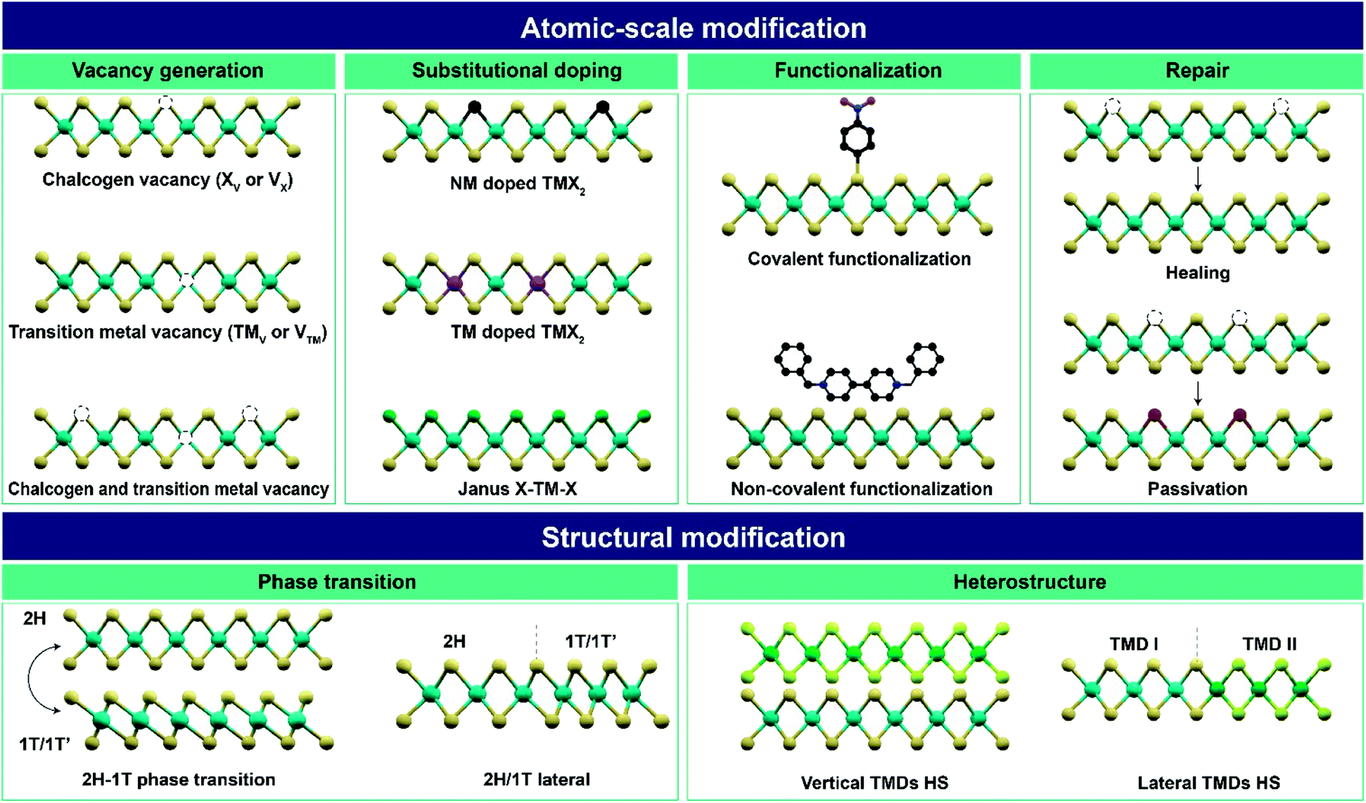 | ||
| Fig. 1 Overview of atomic-scale and structural modifications of 2D TMDs and vdW heterostructures via various post-treatment techniques (X – chalcogen; TM – transition metal; V – vacancy; NM – non-metal; HS – heterostructure). | ||
2. Atomic-scale modification of TMDs
This section details various atomic-scale modifications (namely, vacancy generation, substitutional doping, functionalization, and repair) of TMDs for device applications. In the first sub-section, vacancy generation methods, including plasma treatment, electron-beam irradiation, thermal annealing, and chemical treatment, are introduced for FETs, electrocatalysts, CO2 hydrogenation, and Li–air batteries. The second sub-section describes the substitutional doping of non-metals and metals for applications, such as FETs, biosensors, catalysis, and piezoelectricity. In the third sub-section, covalent and non-covalent functionalizations are discussed for CoVID-19 sensors, triboelectric nanogenerators (TENGs), multifunctional optoelectronic devices, and memory and neuromorphic device applications. The last sub-section describes the repair of atomic defects in TMDs for high-performance flexible piezoelectric nanogenerators (PENGs), photodiodes, superconductors, and low contact resistance in FETs.2.1. Vacancy generation
Vacancy generation in TMDs is highly desirable for controlling the performance of catalytic, electronic, and optoelectronic devices via modulating the carrier concentration and tuning the catalytic activity. The focus in most of the previous studies was chalcogen vacancy generation (hereafter, S and Se vacancies are denoted as SV and SeV, respectively). Vacancy generation can be categorized into (i) dry etching processes, including plasma treatment, electron/ion-beam irradiation, and thermal annealing, and (ii) wet chemical etching processes.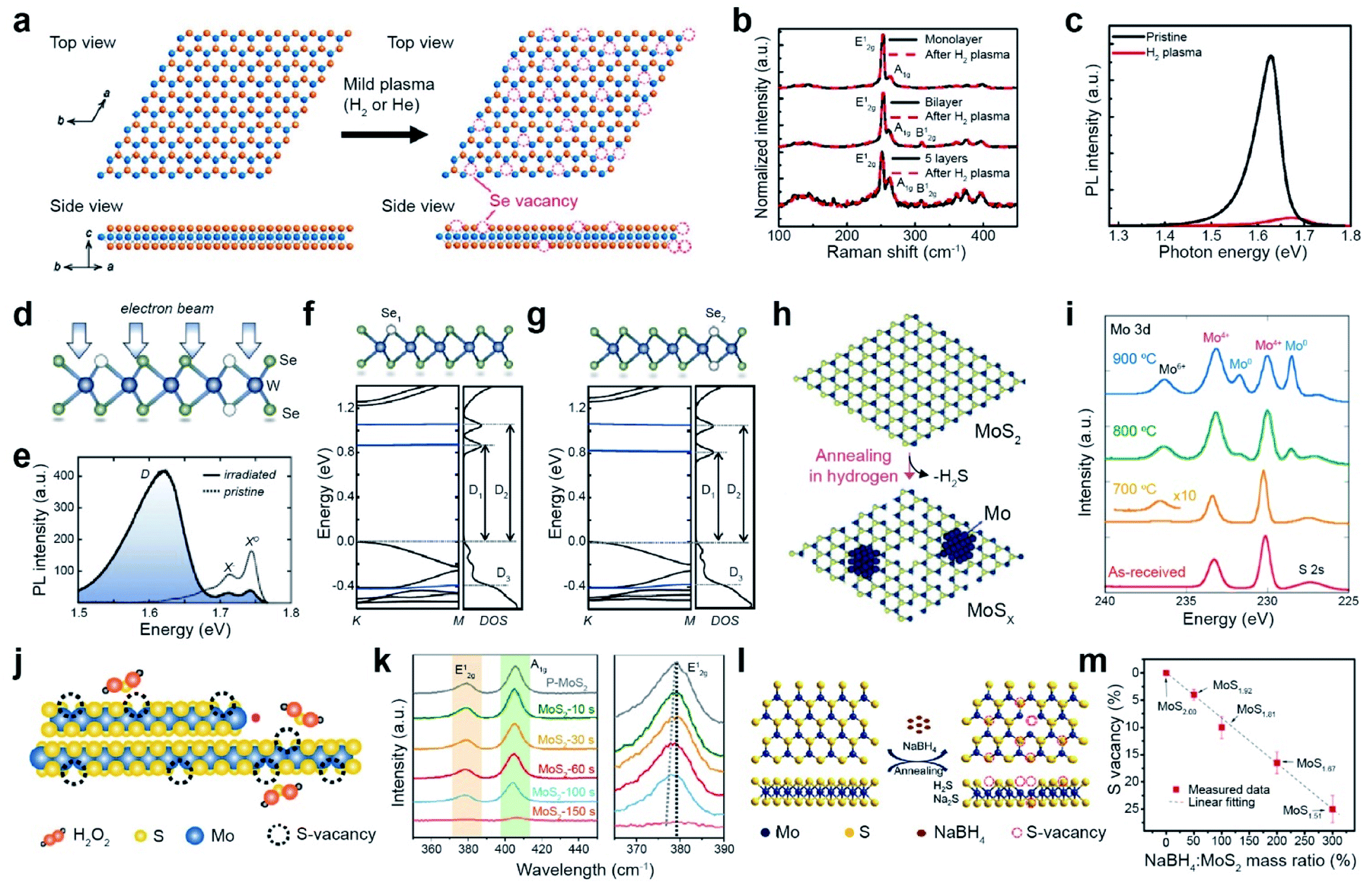 | ||
Fig. 2 Vacancy generation of 2D TMDs with dry (plasma treatment, electron beam irradiation, and thermal annealing) and wet chemical etching processes. Plasma treatment: (a) atomic structure of WSe2 layers before and after the H2 plasma treatment, illustrating the creation of Se vacancies. (b) Raman spectra of monolayer, bilayer, and five-layer WSe2 before and after H2 plasma treatment, respectively. (c) PL spectra of the WSe2 monolayer before and after H2 plasma treatment at room temperature. Electron beam irradiation: (d) illustration of the atomic structure of WSe2 with a single selenium vacancy (Se1) and double selenium vacancy (Se2) after electron beam irradiation. (e) PL spectra of the pristine and electron beam irradiated WSe2, taken at 5 K. (f and g) DFT band structures of Se1 and Se2. Thermal annealing: (h) schematic illustration of the thermal texturization process of MoS2 by thermal annealing under a H2 atmosphere. With increasing SV density, a Mo cluster is also generated. (i) XPS spectra of the Mo 3d core level for as-received and annealed bulk MoS2 samples. Chemical etching: (j) schematic of the chemical etching process with H2O2. (k) Raman spectra of MoS2 with different etching times with H2O2. Right Raman spectra show a red-shift of the E12g peak according to the etching time. (l) Schematic of the desulfurization process of MoS2via solid-phase reduction. (m) SV content variation as a function of mass ratio of NaBH4![[thin space (1/6-em)]](https://www.rsc.org/images/entities/char_2009.gif) :MoS2, obtained from XPS measurement. (a–c) Adapted with permission.27 Copyright 2016, American Chemical Society. (d–g) Adapted with permission.35 Copyright 2021, American Physical Society. (h and i) Adapted with permission.51 Copyright 2016, American Chemical Society. (j and k) Adapted with permission.52 Copyright 2020, American Chemical Society. (l and m) Adapted with permission.54 Copyright 2019, American Chemical Society. :MoS2, obtained from XPS measurement. (a–c) Adapted with permission.27 Copyright 2016, American Chemical Society. (d–g) Adapted with permission.35 Copyright 2021, American Physical Society. (h and i) Adapted with permission.51 Copyright 2016, American Chemical Society. (j and k) Adapted with permission.52 Copyright 2020, American Chemical Society. (l and m) Adapted with permission.54 Copyright 2019, American Chemical Society. | ||
Electron beam irradiation can precisely control the generation of chalcogen vacancies via several mechanisms such as the knock-on effect, ionization, beam-induced chemical etching, and ballistic displacement.33,34 The atomic structure of electron-beam-irradiated WSe2 presents both single (Se1) and double selenium vacancies (Se2) (Fig. 2d).35 The neutral (X0) and negatively charged (X−) exciton peaks of pristine WSe2 are observed in its PL spectra. The additional broad defect band (D) with attenuated X0 and X− intensities are observed for irradiated WSe2 by performing scanning electron microscopy (SEM) with ∼107 electrons per μm2 (Fig. 2e). The density functional theory (DFT) band structures of Se1 and Se2 represent the formation of unoccupied midgap bands (D1 and D2), in addition to the occupied one below the valence-band maximum (D3) (Fig. 2f and g).35 The number of chalcogen vacancies in MoS2 and MoSe2 can be precisely controlled by an electron beam in in situ transmission electron microscopy (TEM).36,37 In addition to electron beams, ion beams such as argon,38,39 helium,40–42 manganese,43 gallium,44,45 and gold,46 can be employed to generate vacancies. For example, the SV content in MoS2 and WS2 monolayers gradually increases with Ar+ ion beam irradiation.47–50
Thermal annealing is a simple method for creating chalcogen vacancies via thermal desorption. A H2 atmosphere is commonly used during thermal annealing to etch away chalcogen atoms via H2S and H2Se formation (Fig. 2h). The thermal texturization process of MoS2 flakes is also observed.51 The XPS spectra of the Mo 3d core level for MoS2 after annealing at elevated temperatures (700, 800, and 900 °C) shows the gradual evolution of peaks at 232 and 229 eV (assigned to the Mo0 doublet) and 236.5 eV (assigned to Mo6+), in addition to a doublet at 233 and 230 eV (assigned to Mo4+ 3d3/2 and 3d5/2, respectively) for pristine MoS2 (Fig. 2i). Such evolution of a Mo0 doublet and Mo6+ peaks is attributed to the formation of Mo metal clusters (by the removal of S atoms) and MoO3 at SV sites (due to Mo oxidation under air), respectively. In contrast, the S 2p doublet in the S 2p core-level spectra is still present, indicating that some MoS2 can be maintained, regardless of the annealing temperature.
:MoS2, indicating that the concentration of vacancies can be efficiently controlled by the amount of reagent (Fig. 2m). Hydrazine is used to donate electrons to WS2, in addition to creating SV.57
Although various types of dry etching processes (i.e. plasma treatment, electron/ion beam irradiation, and thermal annealing) are employed for vacancy engineering, the detailed mechanisms of vacancy generation are still not well-understood. Plasma or ion beams are more desirable for patterned device applications, whereas thermal annealing is preferable for catalytic applications. Chemical wet etching frequently induces the formation of undesired vacancies and oxides.
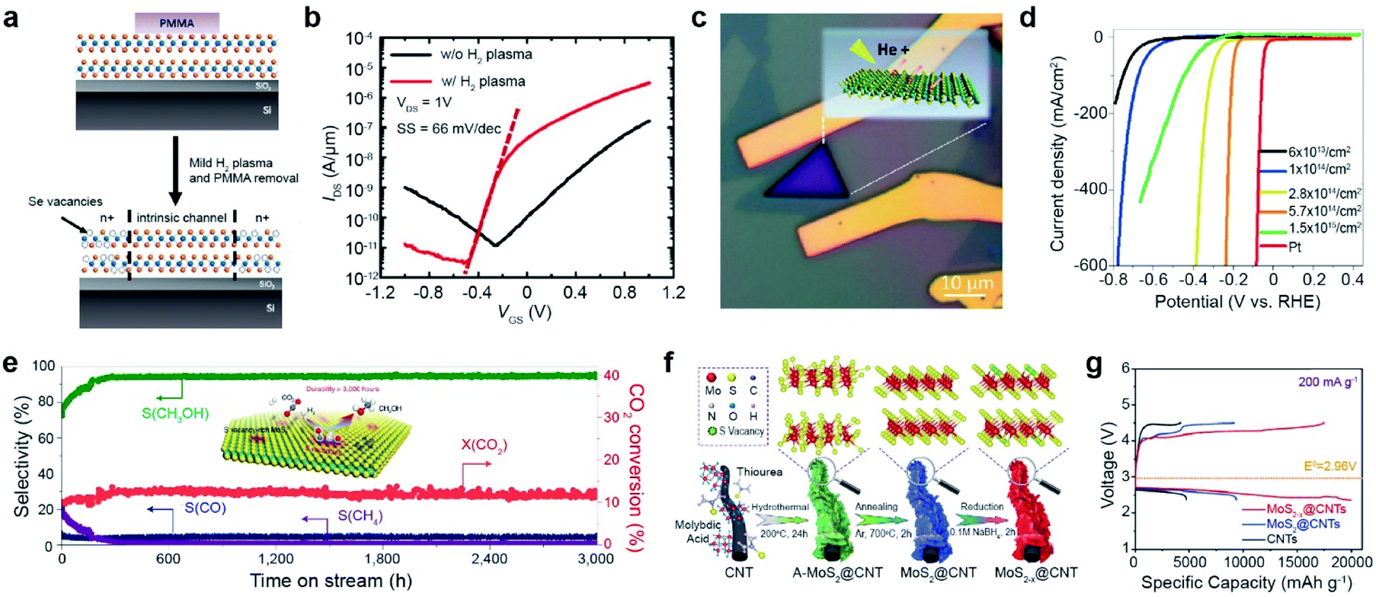 | ||
| Fig. 3 Vacancy-driven applications: FET, electrocatalyst for hydrogen evolution, CO2 hydrogenation catalyst, and Li–air battery. FET: (a) schematic of selective vacancy generation with H2 plasma treatment and (b) corresponding IDS–VGS curves of the WSe2 FET with/without plasma treatment, measured under 1 × 10⁻⁵ Torr. Electrocatalyst for hydrogen evolution: (c) optical image of He+ ion beam irradiated MoS2. (d) LSV curves of MoS2 at various SV concentrations and Pt wire. CO2hydrogenation catalyst: (e) long term stability test of the SV-MoS2 nanosheet catalyst in the hydrogenation of CO2 at 3000 mL gcat.−1 h−1, measuring the selectivity (S) of CH3OH, CO, and CH4 and conversion (X) of CO2 over 3000 h. Li–air battery: (f) synthesis process of MoS2−x@CNTs. (g) Charge/discharge profiles at 200 mA g−1 in the voltage range from 2.35 to 4.5 V. (a and b) Adapted with permission.27 Copyright 2016, American Chemical Society. (c and d) Adapted with permission.68 Copyright 2019, American Chemical Society. (e) Adapted with permission.73 Copyright 2021, Springer Nature Limited. (f and g) Adapted with permission.76 Copyright 2022, Wiley-VCH. | ||
The edge of 2H-MoS2 acts as an active site for hydrogen evolution, whereas the basal plane is inactive.64 In addition, low electrical conductivity limits the electrocatalytic activity of MoS2. Vacancy generation in MoS2 is very useful for activating its basal plane for the hydrogen evolution reaction (HER) and increasing its electrical conductivity.65–67 For example, the basal plane of MoS2 was irradiated with a He+ beam (Fig. 3c). Consequently, with increasing SV concentration, the linear sweep voltammetry (LSV) curves shifted toward the Pt reference up to an optimum concentration of 5.7 cm14 cm−2,68 which is clear evidence of the activation of the basal plane by vacancy generation. When the SV concentration was increased above this threshold, the LSV curves shifted backward (Fig. 3d), attributed to the collapse of the MoS2 structure. Many approaches, including NaClO treatment,69 ozone treatment,70 and laser treatment,71 have been used for vacancy generation to enhance the HER activity of TMDs. In quantum information applications, single-photon emission from the defects of the WSe2 monolayer induced by e-beam irradiation has recently been reported.72
The basal plane of SV-MoS2 is an ideal active site for low-temperature hydrogenation of CO2 to selectively produce methanol via the following reaction mechanism: (i) dissociation of CO2 to surface-bound CO* and O* at SV sites, (ii) hydrogenation of CO* to CH3O*, and (iii) synthesis of CH3OH (inset of Fig. 3e). As a result, SV-rich MoS2 nanosheet catalysts showed a high methanol selectivity of 94.3% and CO2 conversion of 12.5%. Furthermore, they were stable over 3000 h at 180 °C (Fig. 3e).73 SV in MoS2 nanoflowers prepared by thermal annealing in a hydrogen environment also improves solar-driven CO2 photoreduction.74 The rate of CO production was enhanced approximately 2-fold after SV generation.
Chalcogen vacancies provide abundant active sites for the intercalation/deintercalation of guest ions (Li+, Na+, and K+), which leads to enhanced reaction kinetics and improved specific capacities. For example, sulfur vacancies in MoS2 can intrinsically promote O2 adsorption, enhancing the electrochemical performance of Li–O2 batteries.75 The core–shell MoS2−x@CNT composite synthesized by hydrothermal and thermal annealing was treated with NaBH4 to increase SV concentration (Fig. 3f). The initial discharge/charge profile at 200 mA g−1 was significantly boosted up to discharge/charge specific capacities of 19989/17705 mA h g−1 with an overpotential of 0.99/0.26 V (Fig. 3g).76 Furthermore, SV improves polysulfide conversion kinetics in Li–S batteries,77 facilitates the absorption of Na+/Zn+, and increases the conductivity of Na/Zn-ion batteries.78,79
2.2. Substitutional doping
The substitution doping of TMDs is classified into two main categories: impurity doping with partial substitution and Janus structures with full replacement of chalcogen atoms of the top layer (out of three atomic layers) in TMDs. Impurity doping is an important technique for precisely controlling the electrical and other intrinsic properties of TMDs for next-generation high-end electronics, optoelectronics, medicine, and energy harvesting applications.80,81 Several approaches have been developed to tune the characteristics of TMDs by substituting chalcogen atoms (X) or transition metals (M) via atomic doping.82,83 Depending on the relative valency of the dopant atoms, they act as electron donors or acceptors. When a Janus group-VI chalcogenide MXY (top layer X, bottom layer Y = S, Se, and Te; X ≠ Y) is formed, the out-of-plane mirror symmetry is broken. This unique asymmetrical feature of Janus structures arises from different atomic radii and electronegativities of X and Y atoms, thus enabling novel applications such as piezoelectric devices and electrocatalysts.84,85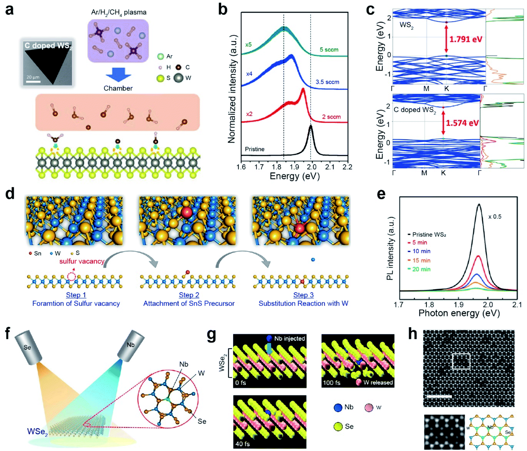 | ||
| Fig. 4 Non-metallic and metallic impurity doping in TMDs: plasma-assisted, thermal annealing, and beam epitaxy. Non-metallic doping: (a) schematic of the plasma-assisted doping experiment (right) and SEM image (left) of the carbon-doped monolayer WS2. (b) PL spectra of the pristine and carbon-doped monolayer WS2 with different methane flow rates (2, 3.5, and 5 sccm, respectively). (c) Band structure and density of states (DOS) of monolayer pristine WS2 and CH-doped WS2. Transition metal doping: (d) doping mechanism of Sn substituting into the W site in the WS2 layers. (e) PL spectrum of monolayer WS2 before and after 5, 10, 15, and 20 min of Sn doping. (f) Schematic representation of Nb doping in WSe2 with a dopant (Nb) and a chalcogen (Se) beam. (g) Snapshots of the Nb substitutional doping process in WSe2 after 0, 40, and 100 fs, respectively, obtained by ab initio molecular dynamics simulation. (h) Representative HAADF-STEM image of monolayer WSe2 after doping of Nb. The scale bar corresponds to 2 nm. Cut out from the white squares is matched with the structural model as shown. In the structural model, blue, green, and yellow balls represent W, Nb, and Se atoms, respectively. (a–c) Adapted with permission.95 Copyright 2019, American Association for Advancement of Science. (d and e) Adapted with permission.101 Copyright 2019, American Chemical Society. (f–h) Adapted with permission.102 Copyright 2021, American Chemical Society. | ||
Transition metal (TM) doping at the M site of a TMD is conducted in three steps: (i) generation of chalcogen vacancies, (ii) replacement of transition metal-adjacent chalcogen vacancy sites, and (iii) healing of chalcogen vacancies.96–100 For example, WS2 monolayers were first grown with SV sites, followed by subsequent exposure to a Sn-rich atmosphere using SnS as a precursor at 550 °C (Fig. 4d).101 The characteristic PL peak of WS2 was gradually attenuated with doping time and dopant concentration (Fig. 4e). Moreover, Sn dopants in the WS2 lattice act as electron donors (i.e., n-type dopants). Another strategy for TM doping is the direct use of a metal flux with the aid of electron beam evaporation (Fig. 4f).97,102 In this case, dopant beams (such as Nb and Re) with low kinetic energy are generated by thermal evaporation of high-melting-point metals on an exposed TMD. The beam flux is modulated to supply metal dopants during the entire doping process to enhance structural reconstruction and regulate the formation of metal-doped TMDs. Concurrently, a Se beam is continuously supplied to heal possible Se vacancies during the doping process. Accurate and position-selective doping can be achieved when patterned TMD materials are used.102 Molecular dynamics (MD) simulations showed a gradual structural change with Nb and Se exposure (Fig. 4g). When a Nb atom hit a W atom with substantial energy (simulation time is varied from 0 to 100 fs), the W atom was released from the original position. Simultaneously, the Nb atom replaced the vacancy created by the released W atom. Fig. 4h displays an atomic-resolution high-angle annular dark-field (HAADF)-scanning transmission electron microscopy (STEM) image of monolayer WSe2 after exposure to a Nb beam. The cutouts from the white squares in Fig. 4h clearly show the atomic structure of Nb-doped WSe2: bright and dark spots at W sites in the hexagonal lattice are assigned to W and Nb atoms (as shown in the structural model). A summary of impurity doping in CVD-grown monolayers and exfoliated TMDs is presented in Table 1.
| Category | Doping sites | Dopants | Host | Type | Doping method | Application | References |
|---|---|---|---|---|---|---|---|
| X | X site | Te | MoS2, WS2 | p | NaOH assisted Te deposition | — | 87 |
| X | X site | Te | MoS2 | — | Te vapor deposition | — | 88 |
| H | X site | Cl | MoS2, MoSe2 | n | Cl ion implantation | Electronics | 89 |
| NM | X site | N | MoS2, WS2 | p | N2 plasma treatment | Electronics | 91 |
| NM | X site | P | MoS2, WS2 | p | PH3 plasma treatment | Electronics | 93 |
| H | X site | F | MoS2 | p | SF6 plasma treatment | Electronics | 94 |
| NM | X site | C | WS2 | p | CH4 plasma treatment | FET | 95 |
| TM | M site | V | MoTe2 | p | Vapor | Ferromagnetism | 96 |
| TM | M site | Nb | WSe2 | p | Molecular beam epitaxy | — | 97 |
| TM | M site | Nb, Co | WSe2 | — | Physical ion implantation | Ferromagnetism | 98 |
| TM | M site | Co | WSe2 | — | Physical ion implantation | Ferromagnetism | 99 |
| TM | M site | Mo/Ti | MoS2, MoTe2 | — | Mo/Ti diffusion | — | 100 |
| TM | M site | Sn | WS2 | n | SnS vapor | Electronics | 101 |
In the past, Janus structures were constructed by a thermal-annealing process under a secondary chalcogen atmosphere. For example, Janus MoSSe and MoSeS structures were produced by annealing MoSe2 and MoS2 at temperatures of ∼800 and ∼450 °C under S and Se atmospheres, respectively.103,104 However, high temperatures are unfavorable for 2D Janus monolayers because of a high probability of alloy or defect formation, such as chalcogen vacancies and cracks.
Remote plasma-assisted chalcogenization consists of two consecutive steps: (i) remote hydrogen plasma treatment of a CVD-grown MoS2 monolayer to strip off sulfur atoms from the top layer and replace them with hydrogen atoms and (ii) replacement of H atoms with Se through a thermal selenization process at ∼450 °C to form a structurally stable Janus MoSSe monolayer (Mo atoms are covalently bonded to the underlying S and top-layer Se atoms) (Fig. 5a).103 Similarly, a room-temperature atomic layer substitution (RT-ALS) process was recently developed (Fig. 5b–i).107 This less disruptive technique employs hydrogen radicals produced by a remote plasma to strip chalcogen atoms on the top layer of an as-grown TMD. Concurrently, vaporized chalcogens (Se or S) are supplied to substitute stripped atoms, resulting in an asymmetric Janus structure at room temperature in the form of MXY (M = Mo or W, X = S or Se, and Y = Se or S). Fig. 5b(ii) depicts the formation of a Janus structure: (I) before H and chalcogen adsorption, (II) adsorption and diffusion of two H atoms to the same S, (III) formation of H2S, (IV) desorption of H2S, and (V) Se occupation of the S vacancy. The free energy values for each step are shown in Fig. 5b(iii). The tilted ADF-STEM image reveals that Se atoms are located on one side of the monolayer MoSSe, while S atoms are on the opposite side. This is direct evidence of a Janus structure (Fig. 5c). The corresponding intensity profile in Fig. 5d clearly shows individual Mo, Se, and S atoms with peak intensities proportional to their atomic numbers. Furthermore, the MoS2 A1g (404 cm−1) and E2g (383 cm−1) modes in the Raman spectra shifted to 288 cm−1 and 355 cm−1, respectively, due to disrupted symmetry in the vertical direction caused by the formation of a Janus structure (Fig. 5e). After further selenization processing of Janus MoSSe was performed, a sharp peak at ∼239 cm−1 and a broad peak at ∼284 cm−1 were formed, which are the signature peaks of the A1g and E2g modes in monolayer MoSe2. In addition, the PL shifts from 1.85 eV (pristine MoS2) to 1.72 eV (Janus MoSSe) and finally to 1.60 eV (converted MoSe2) are clearly observed (Fig. 5f).103,105
 | ||
| Fig. 5 Janus formation via remote plasma-assisted chalcogenization. (a) Atomic structure (top), optical (bottom left), and AFM (bottom right) images of CVD-grown MoS2, hydrogenated MoS2, and Janus MoSSe2 monolayer after two steps of H2 plasma stripping and thermal selenization. (b) (i) Schematic of the room temperature atomic layer substitution (RT-ALS) process of monolayer MoS2. (ii) Schematic of the five key reaction steps in the RT-ALS process (cartoons from left to right): (I) before H adsorption, (II) two H atom adsorption and diffusion to the same S, (III) formation of H2S, (IV) desorption of H2S, and (V) Se occupation of the S vacancy. Purple, yellow, red, and green balls are Mo, S, Se, and H atoms, respectively. (iii) Free energy of each step in B, relative to that of the first step. (c) Tilted STEM image of MoSSe (seen from a vertical direction). Corresponding Mo, Se, and S atoms are shown with blue, red, and yellow circles, respectively. (d) Intensity profile for the atomic structure in the blue box in (c) shows the different intensities of individual Mo, Se, and S atoms. (e and f) Raman and PL spectra of pristine monolayer MoS2, Janus MoSSe, and fully converted MoSe2 respectively. (a) Adapted with permission.103 Copyright 2017, Springer Nature Limited. (b–f) Adapted with permission.107 Copyright 2021, National Academy of Sciences. | ||
Room-temperature doping with remote plasma-assisted chalcogenization offers the possibility of producing high-quality TMDs and 2D Janus structures, which will advance the fabrication techniques for industrial applications as a desirable emerging platform.
Impurity doping is widely used to modulate the electrical properties of TMD materials.91 For example, the I–V transfer curve of n-type-doped multilayer MoS2 obtained by N2 plasma exposure distinctly shows a positive threshold voltage (Vth) shift, which is consistent with the p-type dopant behavior of nitrogen in MoS2 (Fig. 6a). Moreover, Mn-doped MoS2 (Mn-MoS2) was used to selectively detect dopamine (DA) levels in serum and artificial sweat.108 Abnormal levels of dopamine in the body can be symptomatic of several disorders such as Alzheimer's disease, schizophrenia, and Parkinson's disease.109 Previously, DA detection was achieved by employing highly sophisticated methods, such as mass spectrometry, liquid chromatography, and electrochemical detection measurements.110 Therefore, a low-cost but accurate diagnostic tool for the detection of DA levels is essential. A wearable DA sensor was fabricated on a flexible polyimide (PI) sheet with a Mn-MoS2 working electrode (WE), a pyrolytic graphite sheet (PGS) counter electrode (CE), and an Ag paste reference electrode (RE) (Fig. 6b). DA concentrations as low as 50 nM were successfully detected in artificial sweat containing 5 mM glucose (Fig. 6c). Furthermore, Co-doped defective MoS2 (Co-MoS2) exhibits superior dinitrogen-to-ammonia conversion activity compared with pristine MoS2 and CoS2 (Fig. 6d).111 Such a high faradaic efficiency and production rate are attributed to the effective activation of the dinitrogen molecule for the dissociation of the N![[triple bond, length as m-dash]](https://www.rsc.org/images/entities/char_e002.gif) N triple bond in defective MoS2−x.
N triple bond in defective MoS2−x.
 | ||
| Fig. 6 Applications of substitutionally doped TMDs: electronic, biosensor, catalysis, and piezoelectricity. Electronic: (a) schematic of covalent nitrogen doping in MoS2 upon N2 plasma surface treatment (left) and IDS–VGS characteristics of a multilayer nitrogen-doped MoS2 FET (right). Biosensor: (b) assembled integrated sensor for detecting dopamine (DA) levels. (c) Differential pulse voltammetry results with DA in biologically complex samples (artificial sweat containing 5 mM glucose). Nitrogen and CO2reduction catalysis: (d) NRR performance of MoS2−x, Co-doped MoS2−x, and CoS2 at 0.3 V overpotential. Co doping of MoS2−x dramatically increases its faradaic efficiency. CoS2 is inactive for the NRR. (e) Schematic representation of Nb-MoS2 and reduction of CO2 (left), in addition to the calculated CO formation TOF at different applied potentials for Ag NPs, VA-MoS2, and VA-Mo0.95Nb0.05S2 in a CO2 environment (right). Piezoelectricity: (f) schematics and isolated Janus MoSSe monolayers measured by resonance-enhanced piezoresponse force microscopy. HER electrocatalyst: (g) HER polarization curves of monolayer MoS2, MoSe2, SMoSe, and SeMoS. Electronic: (h) four-probe output characteristics (current density (ID/W) versus bias voltage (VM)) with various back-gate voltages (VG) for MoSSe–MoS2. (a) Reproduced with permission.91 Copyright 2016, American Chemical Society. (b and c) Reproduced with permission.108 Copyright 2020, the American Association for Advancement of Science. (d) Reproduced with permission.111 Copyright 2019, American Chemical Society. (e) Reproduced with permission.112 Copyright 2019, American Chemical Society. (f) Reproduced with permission.103 Copyright 2017, Springer Nature Limited. (g) Reproduced with permission.104 Copyright 2017, American Chemical Society. (h) Reproduced with permission.107 Copyright 2021, National Academy of Sciences. | ||
The electrocatalytic conversion of CO2 into sustainable fuels is considered the most efficient approach for achieving carbon neutrality.112 Nb-doped MoS2 can reduce CO2 to produce useful hydrocarbon derivatives, such as methane and ethanol, along with H2 (Fig. 6e). The CO formation turnover frequency (TOF) of Nb-doped MoS2 in an ionic liquid is one order of magnitude higher than that of Ta-doped MoS2 or Ag NPs in the overpotential range of 50–150 mV. Furthermore, the current density of Nb-doped MoS2 in LSV experiments was approximately 2 and 50 times higher than that of pristine MoS2 and Ag NPs, respectively.
The Janus structure of TMDs has been reported to possess piezoelectric properties due to its non-symmetrical structure, which generates electrical polarization in response to externally applied mechanical stress.103 The resonance-enhanced piezoresponse force microscopy image of Janus MoSSe shows the presence of piezoelectric properties (Fig. 6f), which are not observed in pristine MoS2. In addition, Janus TMD monolayers effectively activate TMD basal planes for the HER.104 Janus SMoSe (for MoSSe) and its reverse configuration of SeMoS (for MoSeS) were constructed by atomic substitution of pure MoS2 and MoSe2, respectively (Fig. 6g). Both Janus SMoSe and SeMoS monolayers exhibit lower overpotentials in the LSV curves than pure MoS2 and MoSe2. Moreover, the HER activity of SeMoS surpasses that of SMoSe, which is attributed to the greater thermoneutral Gibbs free energy (ΔGH) for SeMoS in the presence of SeV (−0.007 eV for SeMoS and 0.060 eV for SMoSe). The unique structure of Janus TMDs enables band edge modulation and electronic transfer when heterostructures are designed. Taking advantage of the type-II band alignment of MoSSe–MoS2, a back-gate transistor was fabricated to measure the four-probe output characteristics (Fig. 6h).107 A plot of current density (ID/W) versus bias voltage (VM) at various applied back-gate voltages (VG) shows weak rectification behavior at the lateral junction.
2.3. Functionalization
Functionalization leads to improvement in the optical, electronic, and sensing characteristics of TMDs for next-generation devices. Functionalization with organic molecules is categorized into (i) covalent functionalization via chemisorption and (ii) non-covalent functionalization via physisorption.113,114 Functional groups in an organic molecule effectively tune the Fermi level of TMDs via an electron-donating or electron-withdrawing mechanism. Hydroxyl (–OH), alkoxyl (–OR), and amine groups (–NH2) donate electrons (i.e., they are n-type dopants) to TMDs, while nitro (–NO2), cyano (–CN), and tri-halogenated methyl (–CX3) groups withdraw electrons (i.e., they are p-type dopants) from TMDs.115–118Semiconducting 2H-TMDs, such as MoS2, WS2, and MoSe2, are chemically unreactive because they are free from dangling bonds on their surfaces. However, after the phase transition from 2H to negatively charged metallic 1T-TMDs via lithiation, they become reactive to covalent functionalizations with alkyl halides and diazonium salts (Fig. 7a).119 For example, the MoS2 exciton peak in the PL spectra almost completely disappeared after the phase transition (Fig. 7b) and two prominent peaks evolved in functionalized 1T-MoS2 (Fct-1T-MoS2). The peak at ∼1.6 eV may be attributed to the band structure modification by covalent functionalization, while the peak at ∼1.9 eV is related to the up-shift of the MoS2 exciton emission.119 The appearance of PL peaks indicates that the metallic 1T phase is converted to the semiconducting 1T one after functionalization. This was further confirmed by the characteristics of the fabricated field-effect transistor.
 | ||
| Fig. 7 Covalent functionalization of 2D TMDs: direct functionalization on metallic TMDs, aryl diazonium salt functionalization, and thiol derivative molecule functionalization. Direct functionalization on metallic TMDs: (a) schematic of the conversion of 2H-MoS2 to a negatively charged 1T phase via phase transition using n-butyl lithium (n-BuLi) (top) and subsequent covalent functionalization with alkyl halides (2-iodoacetamide and iodomethane) (bottom). (b) PL spectra of 2H-MoS2, 1T-MoS2 and functionalized MoS2 (Fct-1T-MoS2). Aryl diazonium salt functionalization: (c) schematic representation of MoS2 functionalized by 4-nitrobenzene diazonium (4-NBD) tetrafluoroborate (BF4) via reduction of a diazonium salt, resulting in a nitrophenyl (NP) radical grafting. (d) Schematic illustration of the reaction mechanism of MoS2 with 4-NBD as a function of defect concentration and time. (e) Schematic representation of the direct functionalization of MoS2 with 4-nitrobenzene diazonium (4-NBD) using KI activation. (f) Schematic representation of functionalized 1T′-MoS2 with various diazonium salts including different functional groups (NO2Ph, Cl2Ph, BrPh, MeOPh, and Et2NPh). (g) Work function of functionalized MoS2 with various diazonium salts as a function of the functional group Hammett parameter. Thiol derivative molecule functionalization: (h) schematic representation of the chemisorption of thiol molecules onto SV-MoS2 and the molecular structures of mercaptoethylamine (MEA) and perfluorodecanethiol (FPT). (a and b) Adapted with permission.119 Copyright 2015, Springer Nature Limited. (c and d) Adapted with permission.120 Copyright 2018, American Chemical Society. (e) Adapted with permission.123 Copyright 2021, Royal Society of Chemistry. (f and g) Adapted with permission.125 Copyright 2018, American Chemical Society. (h) Adapted with permission.130 Copyright 2015, American Chemical Society. | ||
Aryl diazonium functionalization can occur at the nearest SV sites of MoS2. SV sites, where charge is accumulated, reduce 4-nitrobenzenediazonium tetrafluoroborate (4-NBD), resulting in nitrophenyl (NP) radical grafting after N2 release (Fig. 7c).120 Localized charge density adjacent to the grafting sites is renormalized after functionalization, further triggering a chain-like growth propagation of subsequent NP molecules over MoS2 sulfur sites (top panels in Fig. 7d). A higher SV density promotes numerous initiation reaction sites for the propagation of NP molecules over the entire MoS2 basal plane (bottom panels in Fig. 7d). The semiconducting nature of MoS2 is still maintained after functionalization. The NP functionalization of SV-MoS2 obeys pseudo-second-order (adsorbate–surface and adsorbate–adsorbate interactions) reaction kinetics,121 whereas the functionalization of Gr obeys first-order (adsorbate–surface interactions) reaction kinetics.122 On the other hand, S sites in MoS2 can be directly functionalized with NP radicals via active chemical reduction of 4-NBD ions, using potassium iodide as an electron donor (Fig. 7e).123 Similarly, alkyl halide-functionalized 1T′-MoS2 is activated using metallocene reducing agents, which facilitate high surface coverage with alkyl halide groups.124 In addition, n-type doping with KI (reducing agent) itself has been observed, providing advantages for low contact resistance and increased charge carrier mobility for FET devices.123
One of the advantages of diazonium salts, in terms of functionalization, is the controllability of the terminated molecules, which enables the engineering of the MoS2 electronic structure. 1T-MoS2 readily reacts with various diazonium salts, including different functional groups (NO2Ph, Cl2Ph, BrPh, MeOPh, and Et2NPh) (Fig. 7f).125 Each functional group has a particular Hammett parameter (Fig. 7g). The measured work function of the functionalized MoS2 increased almost linearly with the Hammett parameter, indicating that the work function of MoS2 can be controlled by functional groups. This surface energy change strongly influences HER catalytic activity. In fact, HER performance is significantly improved by electron-donating Et2NPh groups.125 Furthermore, covalent functionalization of 1T′-MoS2 with Et2NPh improves the stability of electronic transport properties for at least two weeks under atmospheric conditions.126
Another approach is the selective functionalization of TMD chalcogen vacancies or edge sites with thiol derivative molecules via a conjugation reaction.127–129 MoS2 can be functionalized with thiol molecules (2-mercaptoethylamine, MEA, and 1H,1H,2H,2H-perfluorodecanethiol, FDT) at SV sites by soaking for 72 h (Fig. 7f). The charge density of functionalized MoS2 was strongly affected by the terminated molecules. NH2 groups in MEA donate electrons to MoS2 (charge density from 9.4 × 10¹¹ to 1.4 × 1012 cm−2), whereas F groups in FDT withdraw electrons from MoS2 (charge density −7.0 × 10¹¹ to −1.8 × 1011 cm−2).130 Likewise, functionalization with aromatic or alkyl thiols tunes the electronic structure of MoS2. For example, in the case of alkyl thiols, the Fermi energy level (EF) upshifts with increasing chain length, such as for 1-propanethiol, 1-nonanethiol, and 1-dodecanethiol.131
Phase transition requires harsh chemical treatment of TMDs with a highly pyrophoric compound (n-butyllithium), which deteriorates the quality of the material.132,133 The diazonium salt functionalization approach is commonly used to engineer the electronic structure of TMDs. Thiol-derivative functionalization with TMDs is inherently limited by the number of vacancy sites.
Chemical doping of organic molecules on carbon nanotubes (CNTs) and Gr has been extensively studied using two main approaches: (i) modulating the reduction potential of molecules (water bucket model)137 and (ii) controlling electron-donating (e.g., amine, –NH2, and hydroxyl, –OH) and electron-withdrawing groups (e.g., nitro, –NO2, and trihalogenated methyl, –CX3). Analogous strategies have been widely adopted for TMDs. The water bucket model describes the charge transfer between molecules and host materials induced by the difference in reduction potentials. Species with a lower reduction potential give electrons to those with a higher one.137 Material's reduction potential can be calculated by using the following equation: φ/e = V (V vs. SHE) + 4.44 V, where φ, e, V, and SHE denote the work function, electron, reduction potential, and standard hydrogen electrode, respectively.138 For MoS2, the reduction potentials of 0.84 eV (vs. SHE) for 2,3,5,6-tetrafluoro-7,7,8,8-tetracyanoquinodimethane (F4TCNQ) and 0.46 eV (vs. SHE) for 7,7,8,8-tetracyanoquinodimethane (TCNQ) indicate that they withdraw electrons from MoS2 (p-type doping), whereas −0.32 eV (vs. SHE) for nicotinamide adenine dinucleotide (NADH) indicates that they donate electrons (n-type doping) (Fig. 8a).139,140 A drastic enhancement in the PL intensity was observed for MoS2 after functionalization with F4TCNQ and TCNQ (Fig. 8b). In contrast, after functionalization with NADH an attenuation of the PL intensity was detected (Fig. 8c).141 These experimental results demonstrate the EF shift of MoS2 according to p-type and n-type dopants.
 | ||
| Fig. 8 Noncovalent functionalization of 2D TMDs through chemical doping and heterojunction formation. Chemical doping: (a) reduction potentials (vs. SHE) of F4TCNQ and TCNQ for p-type doping and NADH for n-type doping. PL spectra of MoS2 after (b) p-type and (c) n-type doping. (d) Schematic of PFS and AHAPS. (e–g) Schematic of PFS-doped WSe2, AHAPS-doped WSe2, and double-side doped bilayer WSe2 with PFS and AHAPS (top) and their corresponding I–V transfer curves (bottom). Heterojunction formation: (h) illustration of the MoS2/pentacene p–n heterojunction probed by transient absorption spectroscopy. (i and j) Exciton dynamics of a type-II heterojunction. (a–c) Adapted with permission.141 Copyright 2013, American Chemical Society. (d–g) Adapted with permission.142 Copyright 2019, American Chemical Society. (h–j) Adapted with permission.145 Copyright 2017, American Chemical Society. | ||
Molecules with distinct functional groups can be n- or p-type dopants of TMDs. For example, mechanically exfoliated WSe2 flakes were exposed to vapors of trichloro(1H,1H,2H,2H-perfluorooctyl)silane (PFS) with –CF3 functional groups for p-type doping, and N-[3-(trimethoxysilyl)propyl]ethylenediamine (AHAPS) with –NH2 functional groups for n-type doping (Fig. 8d). Before this, however, WSe2 flakes were treated with ozone (UVO3) to improve the functionalization uniformity and ensure high surface coverage. The I–V transfer curves of the WSe2/PFS and WSe2/AHAPS FETs, fabricated on Si/SiO2 with Au contact electrodes, show p-type and n-type characteristics with enhanced hole and electron mobilities of 150 cm2 V−1 s−1 and 17.9 cm2 V−1 s−1, respectively (Fig. 8e and f). Moreover, asymmetric doping obtained by sandwiching bilayer WSe2 with AHAPS (bottom) and PFS (top) shows distinct ambipolar transport properties with electron and hole mobilities of 5.7 cm2 V−1 s−1 and 20 cm2 V−1 s−1, respectively (Fig. 8g).142 To achieve better ambipolar transport characteristics, monolayer WSe2 was subjected to a hybrid functionalization (covalent and non-covalent functionalizations) using two different dopants, 4-NBD and diethylenetriamine. It drastically enhanced the hole and electron mobilities to 82 cm2 V−1 s−1 and 25 cm2 V−1 s−1, respectively.143 In addition, a reduction in the energy bandgap (∼0.24 eV) was observed for WSe2, with asymmetric doping with C60F48 and graphite. This behavior is a consequence of the accumulation of holes and electrons at the bottom and top Se layers.144
Various heterojunctions can be easily constructed by the deposition of organic layers on TMD surfaces. Fig. 8h shows a typical prototype of a type-II organic/TMD heterojunction (pentacene/MoS). When an electron in MoS2 is excited by a photon, a hole is transferred to the p-type pentacene layer within a very short time (τ2 = 6.7 ps) (Fig. 8i). This enables the extension of the interlayer exciton lifetime to as long as ∼5 ns at the pentacene/MoS2 interface (Fig. 8j).145 This dynamic process originates from the quenching of the PL intensity of pentacene/MoS2 when compared to pristine MoS2. Similarly, MoS2/PTCDA, WS2/PTCDA, and MoS2/rubrene also exhibit a type-II p–n heterojunction.134,146,147 Such an extended charge recombination time can improve the quantum efficiency of optoelectronic devices such as diodes, bipolar transistors, photodiodes, and so on.148–150
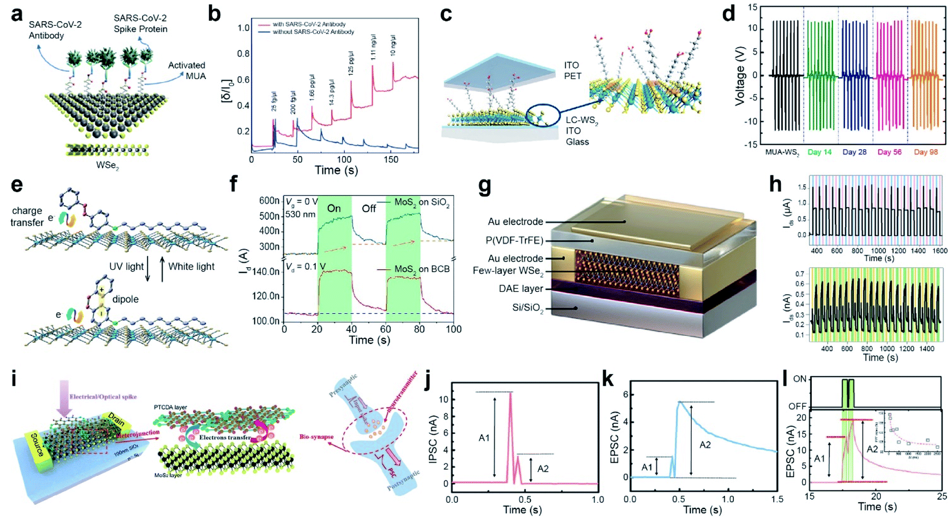 | ||
| Fig. 9 Functionalization for various advanced applications: CoVID-19 sensors, TENGs, multifunctional optoelectronic device, and memory and neuromorphic devices. CoVID-19 sensors: (a) schematic of 11-MUA-functionalized WSe2 for a CoVID-19 sensor. (b) Real-time detection of various SARS-CoV-2 antigen spike proteins with (red curve) and without antibodies (blue curve) using VDS = 1 V and VGS = −0.5 V with a functionalized WSe2 FET. TENGs: (c) Schematic of a ligand-conjugated WS2 TENG device. (d) Output voltages of pristine WS2 and ligand-conjugated WS2 TENG devices. Multifunctional optoelectronic device: (e) schematic of a photomolecular switch device with photochromic molecules (4-(decyloxy)azobenzene) on MoS2. (f) Time-resolved photoresponse of MoS2 FETs on BCB and SiO2 substrates under 530 nm light illumination. Memory device: (g) schematic of the DAE/WSe2/FeFET device. (h) Switching behavior for 20 cycles induced by applying a cyclic ±60 V pulse bias (top) and UV-Vis illumination (bottom). Neuromorphic device: (i) schematic of a MoS2/PTCDA heterojunction operated under both electrical/optical pulses (presynaptic input) and corresponding output current (postsynaptic output). The electron transfer process at the heterojunction interface is analogous to the release of neurotransmitters in biosynapses. (j and k) IPSC/EPSC behavior triggered by a pair of relatively negative Vcg (gate voltage) pulses. (l) EPSC behavior stimulated by a pair of laser pulses. The inset shows the corresponding PPF index A2/A1 as a function of laser pulse interval time. (a and b) Adapted with permission.154 Copyright 2021, American Chemical Society. (c and d) Adapted with permission.158 Copyright 2021, American Chemical Society. (e and f) Adapted with permission.160 Copyright 2019, American Chemical Society. (g and h) Adapted with permission.162 Copyright 2021, Wiley-VCH. (i–l) Adapted with permission.163 Copyright 2019, Wiley-VCH. | ||
With the rapid development of the Internet of Things (IoT), over 50 billion IoT sensors already exist and are expected to surpass 200 billion by 2025.156,157 Among various energy harvesters, TENGs can convert waste mechanical energy into electrical energy under ambient conditions. WS2 nanosheets were functionalized via thiol conjugation reactions at SV sites with various alkanethiol molecules, such as mercaptopropionic acid (MPA), mercaptohexanoic acid (MHA), mercaptooctanoic acid (MOA), and MUA. A TENG device was fabricated using functionalized WS2 and poly(ethylene terephthalate) (PET) as the negative and positive active layers, respectively. Indium tin oxide was used as an electrode (Fig. 9c). Thiol-containing ligands with different alkane chain lengths act as triboelectrification layers in TENGs. A high-precision micromechanical tester was used to press and release a TENG device with a vertical force of 6 N and a frequency of 1 Hz. Pristine WS2 and alkanethiol-functionalized WS2 TENGs exhibited an output voltage of 1.1 V, 8.8 V (MPA), 10.6 V (MHA), 11.4 V (MOA), and 12.2 V (MUA) under open-circuit conditions (Fig. 9d). The MUA-WS2 TENG exhibited a maximum power density of 138 mW m−2. The persistent output voltage of the MUA-WS2 TENG device was maintained after 14, 28, 56, and 98 days, confirming high stability and durability.158 This indicates that alkanethiol functionalization of defective WS2 surfaces via ligand conjugation suppresses reactions with reactive oxygen and reduces the number of catalytically active sites. Moreover, a stable triboelectric output voltage was observed for the MUA-WS2 TENG device even after 10000 cycles. Several 2D materials, including MoS2, WS2, MoSe2, Gr, and Gr oxide (GO)-based TENGs, were fabricated to utilize their triboelectric charging nature. The work functions of the materials decreased in the following order: MoS2 (4.85 eV) > MoSe2 (4.70 eV) > Gr (4.65 eV) > GO (4.56 eV) > WS2 (4.54 eV). Hence, MoS2 is likely to be triboelectrically more negative than the other materials. Furthermore, MoS2 is functionalized with benzyl viologen (BV, n-type) and gold chloride (AuCl3, p-type), resulting in positive and negative values over a triboelectric series (by changing the work function accordingly). These results suggest that triboelectric charging can be tuned through functionalization.159
Another example of the application is a photomolecular switch device, which was fabricated using thin photochromic azobenzene (AZO) physisorbed on MoS2 that was a trap-free benzocyclobutene (BCB)/SiO2/Si substrate (Fig. 9e). The AZO molecules on MoS2 undergo reversible isomerization between the cis and trans states upon exposure to white and UV light illumination, which efficiently modulates the charge transfer process between AZO and the underlying 2D MoS2. The photoresponse of the MoS2 FET device on BCB represents a fast saturation under 530 nm light illumination for 20 s, whereas it shows a steady increase for MoS2 on a SiO2/Si substrate (Fig. 9f). This high response originates from the suppression of the persistent photoconductivity (PPC) effect. Furthermore, a high thermal stability of over 15 h was demonstrated for the photomolecular switching of metastable cis/trans states.160 In addition, a type-II heterojunction phototransistor was developed using an organic phosphonic acid monolayer (12-(benzo[b]benzo[4,5]thieno[2,3-d]thiophen-2-yl)dodecyl) (BTBT) stacked over a MoS2 monolayer. It exhibits an unprecedented responsivity of 475 A W−1 and high external quantum efficiency of 1.45 × 10⁵%. BTBT provides effective charge transfer via π–π interactions and successfully eliminates recombination and charge scattering.161
A ternary-responsive multilevel memory device was fabricated with few-layer WSe2via asymmetric non-covalent functionalization. A photochromic diarylethene (DAE) layer functionalized WSe2 at the bottom, while a ferroelectric poly(vinylidene fluoride-trifluoroethylene) (P(VDF-TrFE)) layer was placed on the top of WSe2 to form a multi-stimuli-responsive Janus WSe2 FET device (Fig. 9g). The device successfully generated two states because of the polarization of P(VDF-TrFE) in the downward/upward direction for a cyclic ±60 V pulse bias. One cycle consisted of +60 V for 2 s (blue region), 0 V for 30 s, −60 V for 2 s (violet region) and 0 V for 30 s (Fig. 9h (top)). Switching with a photochromic DAE was also demonstrated under UV-Vis illumination, where one cycle consisted of 5 s under UV illumination (orange region), 20 s in the dark, 20 s under Vis light (green region), and 20 s without illumination (Fig. 9h (bottom)). Moreover, a multistimuli-responsive asymmetrically functionalized Janus WSe2 device was successfully achieved by modulating the population ratio of polarized P(VDF-TrFE) and photoisomerization DAE. This generated nine unique ferroelectric states and 84 photogenerated states, respectively. The overall maximum of 756 current levels was stored in a single device. The cyclic endurance (10 cycles) and data retention (over 1000 h) confirm the consistency of the device and present high-density non-volatile memory devices.162
A multifunctional neuromorphic device was fabricated via non-covalent functionalization of perylene-3,4,9,10-tetracarboxylic dianhydride (PTCDA) on MoS2, which forms a type-II heterostructure (Fig. 9i). The charge transfer phenomenon between MoS2 and PTCDA mimics neurotransmitter release in biological synapses (right panel of Fig. 9i). The MoS2/PTCDA hybrid synaptic transistor was operated under an electrical field by applying a pair of negative gate voltage (Vcg) pulses (−12 V for 25 ms and −20 V for 25 ms). It exhibited inhibitory post-synaptic current (IPSC) behavior (A2 < A1) and excitatory post-synaptic current (EPSC) behavior (A2 > A1), which correspond to synaptic paired-pulse depression (PPD) and paired-pulse facilitation (PPF) behavior, respectively (Fig. 9j and k). Similarly, a typical EPSC behavior is observed by applying a pair of 532 nm laser pulses (green irradiation with a pulse width of 400 ms, an interval of 100 ms, and a VDS of 0.1 V) (Fig. 9l). Under both operating modes, the type-II MoS2/PTCDA hybrid heterojunction synaptic device performed consistently and successfully mimicked biological synapse functions by an efficient charge transfer process at the hybrid interface.163
2.4. Repair
Atomic chalcogen vacancies in TMDs attenuate their electrical and optical properties (as seen by low PLQY, high Schottky barriers, and limited carrier mobility), which is translated to poor electronic and optoelectronic device performances.164–169 Therefore, the repair of atomic defects is critical for the realization of high-performance devices. Atomic chalcogen vacancies can be repaired using the same chalcogens for healing and other elements for passivation.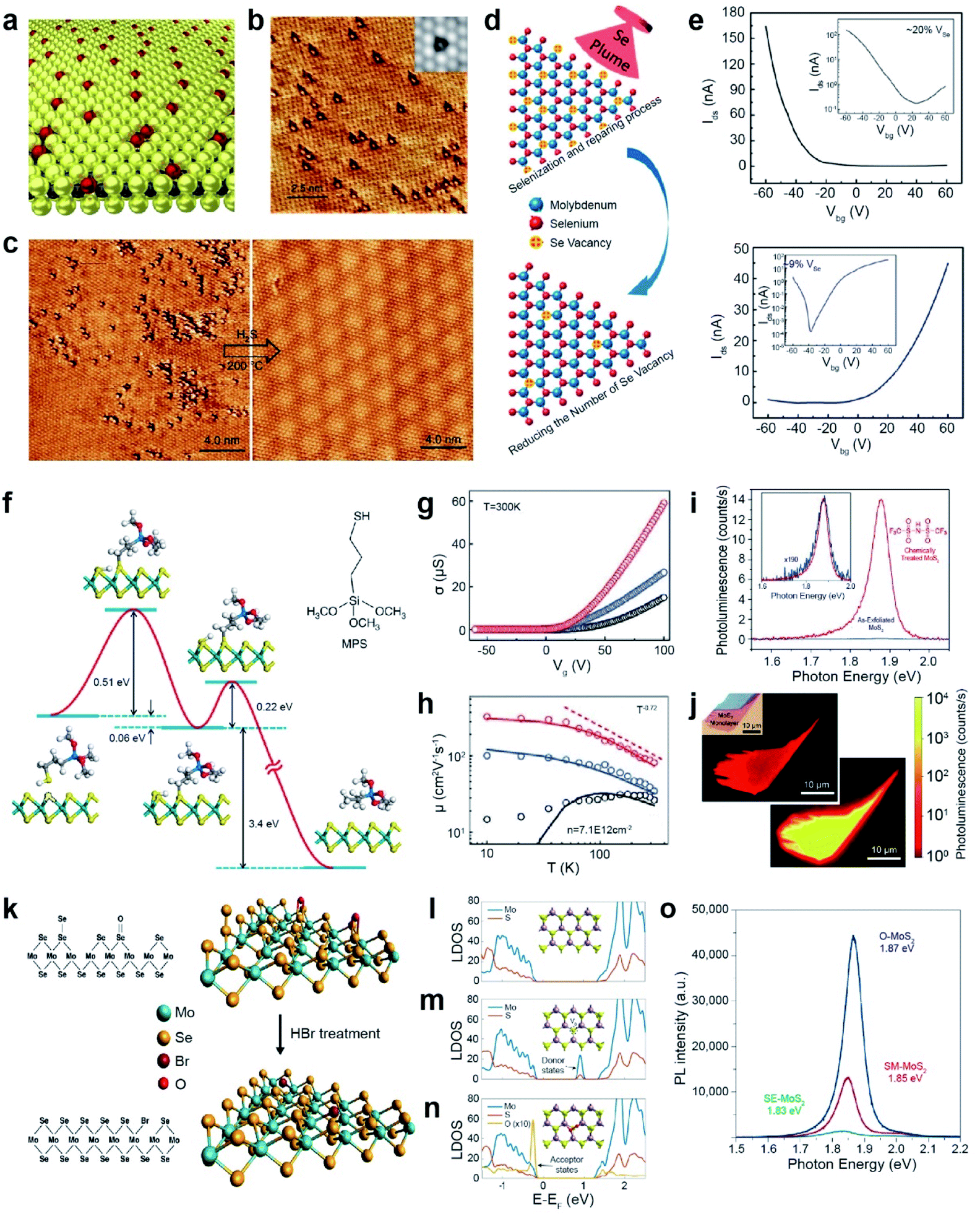 | ||
| Fig. 10 Repair of 2D TMDs: healing and passivation. Healing: (a) schematic representation of atmospheric oxygen atoms getting adsorbed on a MoS2 monolayer. (b) STM image of O atoms (bright spots) absorbed at SV (dark triangles) sites. Inset: simulated STM image. (c) STM images of MoS2 before and after H2S healing at 200 °C. (d) Schematic illustration for post-selenization repair of SeV in MoSe2. (e) Transfer curves of high SeV (∼20%) (top) and healed SeV (∼9%) (bottom) samples. (f) Illustration of reaction pathways for repairing SV-MoS2 using 3-MPS organic molecules. (g and h) Electrical conductance (σ) as a function of gate voltage, carrier mobility and measurement temperature of exfoliated (black), single side treated (blue) and double side treated (red) samples. (i) PL spectra of exfoliated MoS2 (blue) and TFSI-treated MoS2 (red). The inset shows the 190× magnified PL spectra of as-exfoliated MoS2. (j) Confocal PL mapping image of exfoliated MoS2 (top) and TFSI-treated MoS2 (bottom). Passivation: (k) schematic of SeV passivation with Br in MoSe2 by HBr treatment and the corresponding atomic structures. (l–n) LDOS of (l) pristine MoS2 (top), (m) SV-MoS2 (middle), and (n) O-MoS2 (bottom). (o) PL spectra of SE-MoS2, SM-MoS2, and O-MoS2 grown under oxygen conditions (O-MoS2), sulfur-mild conditions (SM-MoS2) and sulfur-excess conditions (SE-MoS2), respectively. (a–c) Adapted with permission.173 Copyright 2018, Springer Nature Limited. (d and e) Adapted with permission.174 Copyright 2016, American Chemical Society. (f–h) Adapted with permission.177 Copyright 2014, Springer Nature Limited. (i and j) Adapted with permission.180 Copyright 2015, American Association for the Advancement of Science. (k) Adapted with permission.182 Copyright 2016, American Chemical Society. (l–o) Adapted with permission.186 Copyright 2022, Springer Nature Limited. | ||
The post-selenization process is performed on defected monolayer MoSe2via pulsed laser vaporization of selenium to repair SeV (Fig. 10d). The temperature plays a crucial role in selenization, where the optimum temperature range is between 600 and 700 °C. The I–V transfer curves show major carrier type conversion from p-type characteristics for high Se vacancies (∼20% VSe) to n-type characteristics for healed Se vacancies (∼9% VSe). Moreover, the obtained hole and electron mobilities were ∼0.011 and 0.021 cm2 V−1 s−1, respectively (Fig. 10e).174 Selective post-sulfuration on patterned MoSe2 readily forms MoSe2/MoS2 heterojunctions and exhibits a type-I band alignment.175
Another healing method for SV in MoS2 (SV-MoS2) involves the use of S-containing organic molecules.176 For example, SV-MoS2 was coated with 3-mercaptopropyl trimethoxysilane (MPS) and subsequently annealed at 350 °C under a H2/Ar atmosphere. The healing process involves the following reaction: HS(CH2)3Si(OCH3)3 + SV-MoS2 → CH3(CH2)2Si(OCH3)3 + MoS2. The reaction kinetics of SV-MoS2 and MPS involve two representative steps of chemical adsorption between SV and thiol groups in MPS and dissociation of the S–C bond with an energy barrier of 0.51 and 0.22 eV, respectively (Fig. 10f). The SV density was dramatically reduced from ∼6.5 × 10¹³ to ∼1.6 × 1013 cm−2, for topside MPS treatment. Electrical transport properties were measured for three FET samples on Si/SiO2: exfoliated MoS2 (black), top-side-treated MoS2 (blue), and double-side-treated MoS2 (red) (Fig. 10g). The double-sided MPS treatment further reduced short-range scattering and charge impurities and thus enhanced the carrier mobility of 81 cm2 V−1 s−1 at room temperature.177 The carrier mobility of these samples at low temperature (10 K) was further increased to 14 cm2 V−1 s−1, 106 cm2 V−1 s−1, and 320 cm2 V−1 s−1, respectively (Fig. 10h). The catalytic properties of MPS-treated MoS2 drastically decrease due to the depletion of electrochemically active sites, thereby increasing the overpotential and the Tafel slope.178
As an alternative, bis(trifluoromethane) sulfonamide (TFSI) was employed to heal SV in MoS2 and WS2.179 The exfoliated MoS2 that was treated with TFSI exhibited a 190-fold increase in the magnitude of the PL peak intensity (Fig. 10i), consisting of a brighter PL image than that of the pristine one (Fig. 10j).180 An increased quantum yield QY (>95%) and longer lifetime (∼10 ns) were also observed due to the elimination of the non-radiative recombination. TFSI-treated MoSe2 and WSe2 exhibited a moderately reduced QY. TEM analysis revealed that SeV sites in WSe2 were not passivated by S atoms.181
The healing of atomic chalcogen vacancies using organic thiol molecules is still under debate. Three possible reaction mechanisms include repair, functionalization, and dimerization.187 The energy barrier rate-determining steps for both functionalization and repair mechanisms are almost similar, indicating that these are competing reactions.188 Moreover, numerous factors, such as the nature of thiol molecules, concentration of SV, reaction temperature, and time, are critical in determining the reaction mechanism. Furthermore, thiophenol molecules (C6H5SH) can heal and adsorb on SeV in WSe2. The adsorbed thiophenol molecule displays a vertical configuration, which is consistent with experimental STM images.189 The mechanisms of defect passivation and/or healing are still not clearly understood for TFSI-treated TMDs. TFSI treatment increases the PL lifetime but limits the carrier mobility by the charge scattering mechanism.181,190 In order to overcome this issue, exfoliated MoS2 and WS2 were first treated with thiol molecules (3-n-octylthiophene, dipropyl sulfide, or ethanethiol) to control SV, followed by TFSI treatment. The two-step treatment effectively eliminates sub-gap states and lowers the Fermi level, which greatly improves the PL lifetime and enhances carrier mobility.191
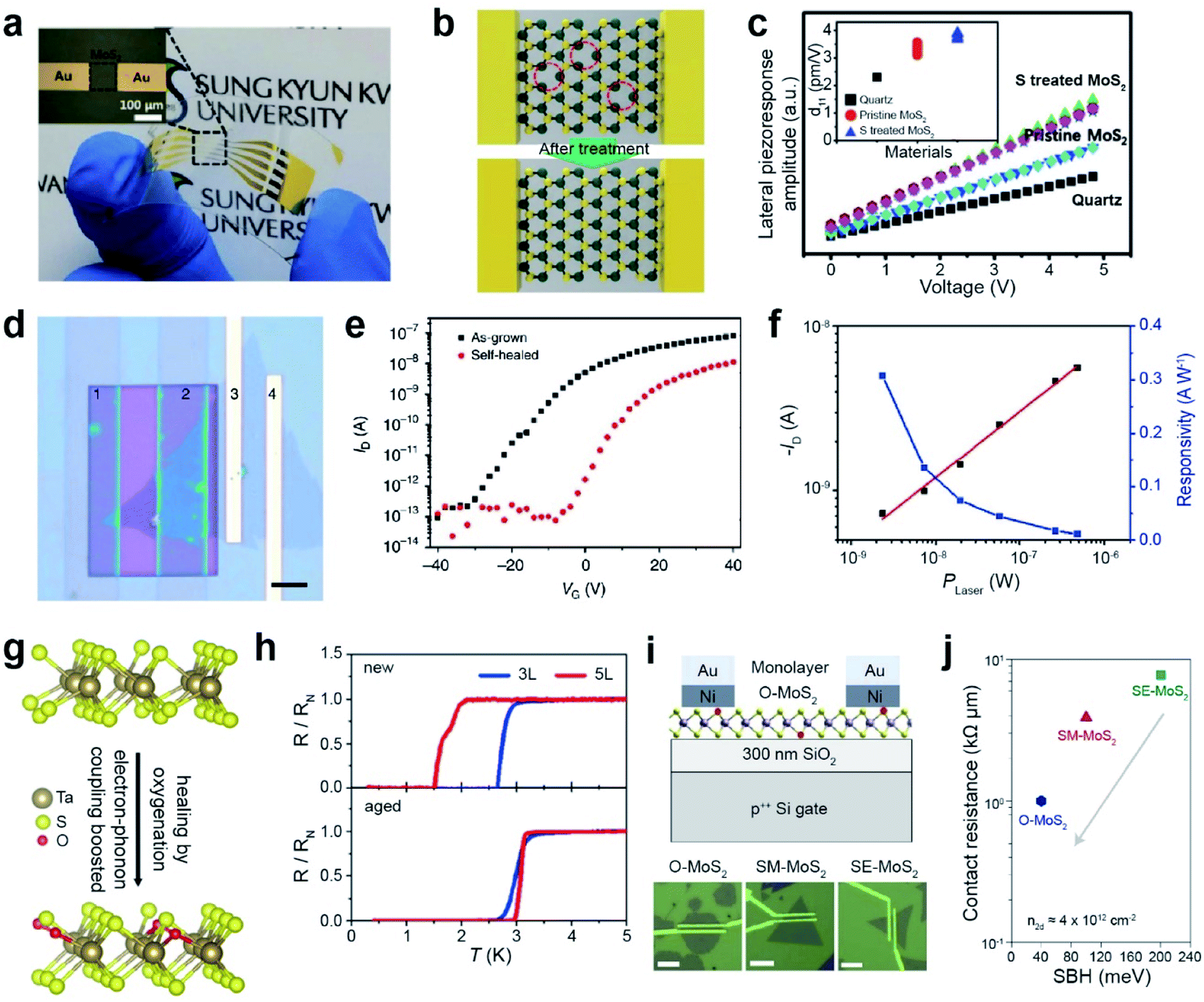 | ||
| Fig. 11 Repair-based various applications: PENG, photodiode, superconductors, and contact resistance in FETs. PENG: (a) photograph of a flexible PENG device on a PET substrate. (b) Schematic of SV healing in MoS2via H2S treatment. (c) Lateral piezoelectric effect of quartz, SV-MoS2, and SV-treated MoS2 samples. Photodiode: (d) optical image of (1–2) a selectively self-healed (PEDOT:PSS) MoS2 FET, (2–3) a self-healed MoS2/as-grown MoS2 homojunction, and (3–4) as-grown MoS2 FET devices (scale bar: 5 μm). (e) I–V transfer curve of as-grown MoS2 (black) and self-healed MoS2 (red). (f) Photocurrent and responsivity on the (2–3) MoS2 homojunction device. Superconductors: (g) schematic of oxygen passivated TaS2. (h) Normalized resistance as a function of temperature for new and aged (after 3 weeks) devices. Contact resistance in FETs: (i) schematic of the as-fabricated oxygen-rich MoS2 (O-MoS2) FET on SiO2/Si and the corresponding optical images of O-MoS2, SM-MoS2 and SE-MoS2 with a 1 μm channel length. (j) Contact resistance (RC) versus Schottky barrier height (SBH) for the three devices. (a–c) Adapted with permission.193 Copyright 2018, Wiley-VCH. (d–f) Adapted with permission under a Creative Commons CC-BY License.194 Copyright 2017, Springer Nature Limited. (g and h) Adapted with permission.198 Copyright 2020, American Chemical Society. (i and j) Adapted with permission.186 Copyright 2022, Springer Nature Limited. | ||
A photodiode was fabricated using selective healing of patterned MoS2. Self-healing is carried out by the hydrogenation of poly(3,4-ethylenedioxythiophene)–poly(4-styrenesulfonate) (PEDOT:PSS). Fig. 11d displays the optical image of the selectively healed MoS2 FETs, where regions 1 and 2 are healed MoS2, regions 3 and 4 are as-grown MoS2 FETs, and regions 2 and 3 indicate homojunctions. The transfer characteristics of the as-grown MoS2 and self-healed MoS2 are shown in Fig. 11e. VT shifted toward zero after self-healing, indicating unipolar n-type electrical transport behavior. The MoS2 homojunction photodiode exhibits a high photoresponsivity of 308 mA W−1 (observed at zero source-drain bias) with excellent air stability (Fig. 11f), as a result of efficient electron–hole separation at the homojunction.194
Recently, research on ultrathin superconductors has been exclusively conducted after the advancement in exfoliation (from bulk down to monolayer) and encapsulation techniques of 2D materials. However, monolayer TMDs possess a high density of defects, eventually resulting in the localization of Cooper pairs and decreasing transition temperature (Tc) for metal-to-insulator transitions.195–197 SV sites in ultrathin TaS2 are passivated by oxygen to form oxygenated TaS2 in air (Fig. 11g). Theoretical calculations predict that oxygen passivation in monolayer TaS2 significantly decreases the carrier density of pure TaS2. Transport measurements were performed for three- (3L) and five-layered (5L) TaS2 devices, either in a fresh (denoted by new) or oxygenated (denoted by aged) form (Fig. 11h). The Tc values of both 3L and 5L TaS2 increase with oxygen, owing to the increase in electron–phonon coupling.198
FETs were fabricated using three different types of monolayer MoS2: those grown under oxygen conditions (O-MoS2), mild sulfur conditions (SM-MoS2), and excess sulfur conditions (SE-MoS2) (Fig. 11i). The I–V transfer curves of O-MoS2 display a positive Vth (+21.0 ± 4.6 V), whereas a negative Vth was observed for SE-MoS2 (−17.0 ± 9.7 V) and SM-MoS2 (2.8 ± 4.9 V). The contact resistance (RC) of the three devices was determined using the Schottky barrier height (SBH) at the interface (Fig. 11j).186 The O-MoS2 FET exhibits a low RC value of ∼1 kΩ μm, whereas high RC values of 3.9 and 7.8 kΩ μm are observed for SM-MoS2 and SE-MoS2 FETs, respectively (at the same carrier density (n2D) of 4 × 1012 cm−2). This is ascribed to the reduced SBH in O-MoS2 owing to the absence of donor states and the Fermi level closer to the CBM of MoS2.
3. Structural modification
This section presents a discussion on two structural modifications of TMDs for various device applications: (i) phase transition and (ii) heterostructure formation. In the first sub-section, the structural phase transition from trigonal prismatic 2H to octahedral 1T or distorted 1T′ is addressed, with potential applications in wireless energy harvesting, solar cells, electrocatalysts, Li-ion batteries, and memory and neuromorphic devices. In the second sub-section, the construction of vertical van der Waals and lateral heterostructures is described, with several applications, such as photocatalysts, photodetectors, solar cells, magnetic applications, and sensors.3.1. Phase transition
TMDs exist in a wide range of crystalline phases, from trigonal prismatic 2H to octahedral 1T or distorted 1T.199 The stability and the free energy between the phases differ, depending on the material. For example, 2H-MoS2 is more stable than 1T′-MoS2 under ambient conditions and the free energy difference between the two phases is very large (ΔE > 0.8 eV). In contrast, MoTe2 exhibits a small free energy difference (ΔE < 50 meV) between the 2H and 1T′ phases.200,201 Therefore, techniques for phase transition are unique for each material. Metallic phase accelerates the electron transport to obtain low contact resistance of FETs and enhances their performance in electrocatalysis, supercapacitors, and batteries.Li intercalation effectively reduces the energy barrier of the phase transition from 2H-MoS2 to 1T-MoS2 and stabilizes the metallic phase.202n-Butyllithium in hexane was employed for Li intercalation in MoS2 and it induced a phase transition from 2H to 1T. This was followed by sonication of LiMoS2 to exfoliate 1T MoS2 (∼1–3 nm film) in water (Fig. 12a).203 The 1T-MoS2 thin films, prepared by drop-casting on a DVD disc, were reverted to the 2H phase by IR laser irradiation, as confirmed by XRD (Fig. 12b). The characteristic (002) peaks for 2H-MoS2 disappeared after 60 min, and new diffraction peaks (indicated by stars) appeared, which correspond to the 1T phase. Furthermore, electrochemical lithiation has been proposed to replace the flammable and dangerous n-butyllithium. Li foil and MoS2 were used as anodes and cathodes, respectively.204,205 Alternatively, alkali metals (lithium, potassium, or sodium) and naphthalene can be used for phase transitions.206–209
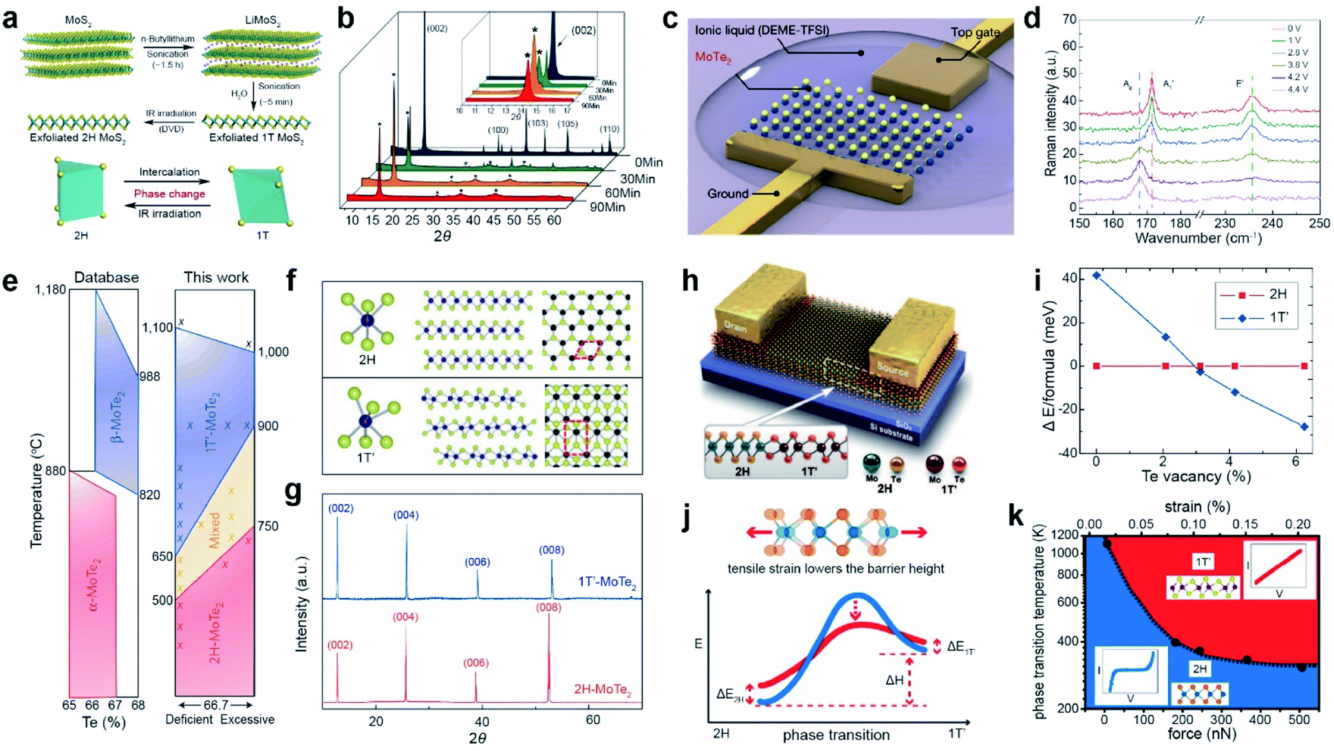 | ||
| Fig. 12 Phase transition of 2D TMDs with Li intercalation, electrostatic doping, thermal annealing, laser, and tensile strain. Li intercalation: (a) schematic illustration of Li intercalation into MoS2. (b) XRD patterns obtained during the sonication-assisted lithium intercalation of MoS2 for different times. Electrostatic doping: (c) schematic of a monolayer MoTe2 FET. (d) Raman spectra of phase transition from the 2H to the 1T′ phase with bias changed from 0 V to 4.4 V. Thermal annealing: (e) phase diagram of MoTe2 from the ASM alloy phase diagram database (left) and the new phase diagram based on experiment (right). (f) Ball-and-stick models for 2H- and 1T′-MoTe2. (g) XRD patterns of 1T′-MoTe2 (blue) and 2H-MoTe2 (red) single crystals. Laser treatment: (h) schematic of a 1T′/2H MoTe2 homojunction device. (i) DFT-calculated energy difference between the 2H and 1T′ phases as a function of TeV concentration. Tensile strain: (j) schematic of the strain-dependent phase transition barrier. (k) Temperature- and force-dependent phase diagram of semiconducting 2H and metallic 1T′ MoTe2. (a and b) Adapted with permission.203 Copyright 2011, American Chemical Society. (c and d) Adapted with permission.210 Copyright 2017, Springer Nature Limited. (e–g) Adapted with permission.216 Copyright 2015, Springer Nature Limited. (h and i) Adapted with permission.222 Copyright 2015, American Association for the Advancement of Science. (j and k) Adapted with permission.224 Copyright 2016, American Chemical Society. | ||
A low free energy difference (<50 meV) between the 2H and 1T′ phases in MoTe2 enables a reversible phase transition. For example, electrostatic doping with an ionic liquid (N,N-diethyl-N-(2-methoxyethyl)-N-methylammoniumbis(trifluoromethyl sulphonyl-imide) and DEME-TFSI) gating in a FET triggers a reversible phase transition (Fig. 12c).210,211 The Raman spectra of MoTe2 exhibit the gradual disappearance of the A′1 mode (171.5 cm−1) and E′ mode (236 cm−1) of 2H MoTe2 with increasing gate voltage from 0 V to 4.4 V, in addition to the appearance of the Ag mode (165.5 cm−1) of 1T′ MoTe2 (Fig. 12d). A fully reversible phase transition of MoTe2 can be achieved by increasing or decreasing the gate voltage. Similarly, the electrochemical phase transition of MoTe2 (from a monolayer to a 73 nm thick sample) was achieved using ionic liquid gating at room temperature in air.212 The phase transition of T-TaS2 (from T to H) and NbSe2 (from 2H to 1T) was achieved by applying a high bias voltage under a scanning tunneling microscope (STM) tip at low temperatures.213,214 The high density of electron doping from the 2D electrode [Ca2N]+·e− drives the phase transition from the 2H to the 1T′ phase in a long MoTe2 (up to ∼100 nm) sample.215
In addition, the phase diagram of MoTe2 indicates that the phase stability of 2H and 1T′ strongly depends on temperature and Te deficiency (Fig. 12e). Only the 1T′ phase was obtained by rapid cooling at 900 °C during the flux synthesis process, whereas the 2H phase was obtained by slow cooling to room temperature, as confirmed by XRD patterns (Fig. 12f and g).216 On the other hand, a phase transition from 1T′ to 2H MoTe2 has been demonstrated with thermal annealing at 650 °C under a Te rich atmosphere.217 Recently, single-crystal multilayer 2H MoTe2 films were successfully synthesized via a phase transition from a polycrystalline multilayer 1T′ MoTe2 film initiated from single-crystal 2H MoTe2 seeds.218 The phase transitions of other TMDs, such as TaS2, PtSe2, and PdSe2, were also demonstrated with thermal annealing processes.219–221
A homojunction between the 2H and 1T′ phases in the MoTe2 FET was realized by a laser-driven phase transition (Fig. 12h). The metallic 1T′ phase was induced by selective laser irradiation of the 2H region to introduce Te vacancies (Fig. 12i). This homojunction in MoTe2 FET devices significantly reduces the contact resistance by forming an ohmic contact between the 1T′ and 2H regions.222 Similarly, the metastable 1T/1T phase of MoS2 is changed to a stable 2H phase via continuous-wave laser and femtosecond pulsed laser radiation.223
The introduction of strain is another strategy for inducing a phase transition. The tensile strain lowered the barrier height for the phase transition from 2H-MoTe2 to 1T′-MoTe2 (Fig. 12j). The temperature is further required to overcome the energy barrier for the phase transition under tensile strain (Fig. 12k). Experimentally, the reversible phase transition between 2H and 1T′ of MoTe2 was confirmed using an atomic force microscope (AFM) tip.224 Supercritical CO2 treatment can also induce a phase transition in TMDs via the formation of local strain in MoS2.225,226 A chalcogen vacancy is also used to induce local strain, resulting in the spatial phase transition of MoS2 and PdSe2.227,228
Phase transitions in TMDs can be achieved by alkali metal intercalation, electrostatic doping, electron transfer, thermal treatment, external irradiation, and strain. A summary of the phase transitions of the TMDs is listed in Table 2. Reversible phase transition between 2H and 1T (1T′) can be induced by Li intercalation/annealing as well as ionic liquid gating. However, Li intercalation, plasma treatment, and supercritical CO2 can't reach 100% yield of metallic phase TMDs.
| Materials | Phase | Methods | Application | References |
|---|---|---|---|---|
| MoS2 | 2H → 1T | Li intercalation | — | 203 |
| MoS2 | 2H → 1T | Na and naphthalenide intercalation | — | 206 |
| MoS2 | 2H → 1T′ | Li intercalation | — | 207 |
| MoS2 | 2H → 1T | Electrochemical Li | HER | 208 |
| MoS2 | 2H → 1T/1T′ | K intercalation | — | 209 |
| MoTe2 | 2H → 1T′ | Electrostatic doping | — | 211 |
| NbSe2 | 2H → 1T | Electrostatic doping | — | 214 |
| MoTe2 | 2H → 1T′ | Electron transfer ([Ca2N]+·e−) | — | 215 |
| MoTe2 | 2H → 1T′ | Thermal treatment | — | 216 |
| TaS2 | 1T → 2H | Thermal treatment | — | 219 |
| PtSe2 | 1T ↔ 1H | Thermal treatment | — | 220 |
| MoTe2 | 2H → 1T′ | Laser irradiation | FET | 222 |
| MoS2 | 1T/1T′ → 2H | Laser irradiation | — | 223 |
| MoTe2 | 2H → 1T′ | Tensile strain (AFM tip) | — | 224 |
| MoS2 | 2H → 1T′ | Supercritical CO2 | HER | 225 |
| MoS2 | 2H → 1T | Ar plasma | FET | 227 |
| MoS2xSe2(1−x) | 2H → 1T | Electrochemical Li | Solar cell | 231 |
| MoS2 | 2H → 1T | Li intercalation | Supercapacitor | 238 |
| WS2/Gr | 2H → 1T | Li intercalation | Supercapacitor | 239 |
| MoS2 | 2H → 1T′ | Li intercalation | Neuromorphic computing | 241 |
| WS2 | 2H →1T | Li intercalation | HER | 243 |
| ReS2xSe2(1−x) | 2H →1T′ | Li intercalation | HER | 248 |
| MoSe2 | 2H →1T | Li intercalation | HER | 249 |
For wireless energy harvesting from the Wi-Fi band (2.45 and 5.9 GHz), a rectifier device is fabricated using MoS2 on a flexible Kapton substrate. Fig. 13a illustrates a lateral MoS2 semiconducting–metallic (2H–1T/1T′) Schottky diode with palladium and gold layers forming Schottky and ohmic contacts, respectively. Nonlinear I–V characteristics were observed for a given input radio frequency (RF) power owing to the presence of a Schottky junction between Pd and 2H-MoS2, which is attributed to the rectification behavior. For an input RF power of 5 mW, the device exhibited a cutoff frequency of 10 GHz and an output voltage of 3.5 V, because of the rectified voltage increase (Vout) (Fig. 13b). Hence, a high cut-off frequency is sufficient to cover both Wi-Fi bands.229 A flexible Wi-Fi band antenna integrated with a MoS2 phase junction (2H–1T/1T′) Schottky diode can achieve wireless energy harvesting of electromagnetic radiation, which is efficiently used for self-powered systems.
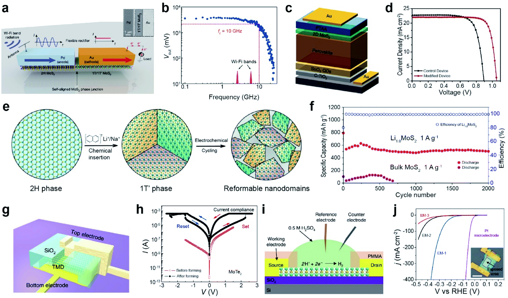 | ||
| Fig. 13 Phase transition for various applications: wireless energy harvesting, solar cell, Li-ion battery, resistive memory, and electrocatalytic applications. Wireless energy harvesting: (a) schematic of a lateral MoS2 semiconducting–metallic (2H–1T/1T′) Schottky diode with palladium and gold layers forming a Schottky and an ohmic contact, respectively. The antenna receives a Wi-Fi signal and converts it into an AC signal. The Schottky MoS2 diode rectifies the AC signal to the DC one. (b) Device output voltage as a function of frequency. Solar cell: (c) scheme of a solar cell architecture. (d) J–V curves of CsFAMA devices. Li-ion battery: (e) schematic of crystalline domain formation after chemical lithiation of bulk 2H-MoS2. (f) The cycling performance of Li1.0MoS2 and bulk MoS2 at 1 A g−1 for 2000 cycles, respectively. Resistive memory: (g) schematic of a vertical MoTe2 resistive random access memory (RRAM) device. (h) I–V curves of a MoTe2 RRAM device with a flake thickness of 24 nm and an area of (520 nm × 330 nm). Bipolar resistive switching behavior of MoTe2 before (red) and after (black) formation. Arrows indicate the sweep direction. HER electrocatalyst: (i) schematic of the electrochemical microcell for HER measurements. (j) Polarization curves of the current density obtained with EM-1, EM-2 and EM-3. (a and b) Adapted with permission.229 Copyright 2019, Springer Nature Limited. (c and d) Adapted with permission.230 Copyright 2020, Elsevier B.V. (e and f) Adapted with permission under a Creative Commons CC-BY License.233 Copyright 2016, American Chemical Society. (g and h) Adapted with permission.240 Copyright 2019, Springer Nature Limited. (i and j) Adapted with permission.245 Copyright 2018, Springer Nature Limited. | ||
A perovskite solar cell was fabricated with 1T-MoS2 as the hole transport layer (HTL) in the device architecture of FTO/c-TiO2/SnO2QD/Cs0.1FAPbI3(0.81)MAPbBr3(0.09)/MoS2/PTAA/Au (Fig. 13c). 1T-MoS2 reduced the mismatch between the energy-band alignment and trap density of perovskite, which increased the carrier concentration and improved the fill factor. The power conversion efficiency (PCE) of 1T-MoS2 increased from 15.05% to 18.54% (Fig. 13d).230 In other work, a single-layer MoS2xSe2(1−x) nanosheet with the 1T phase (≈66%) was synthesized by electrochemical Li intercalation and exfoliation. The metallic 1T MoS2xSe2(1−x) phase facilitates electron transport to the counter electrode surface in dye-sensitized solar cells (DSSCs).231 A higher PCE of 8.94% with 1T-MoS2@HCS (hollow carbon sphere) was attained compared to those of 2H-MoS2@HCS (8.16%) and Pt (8.87%).232
Metallic-phase TMDs are promising electrodes for metal-ion batteries. Electrochemical cycling for the phase transition from bulk 2H-MoS2 to 1T′-LixMoS2via Li intercalation/deintercalation induced the formation of reformable nanodomains (Fig. 13e). Li1.0MoS2 showed a high specific capacity of 636 mA h g−1 at 1 A g−1 with a capacity retention of 80% and coulombic efficiency of 100%, whereas the capacity of bulk MoS2 collapsed very sharply (Fig. 13f). The domain boundaries between nanodomains facilitate the mass transport of Li+ ions and charge/discharge reaction: S + 2Li+ + 2e− ↔ Li2S.233 Another example is the TiO–1T-MoS2 nanoflower composite for Na-ion batteries, which exhibits a high reversible capacity, attributed to the well-distributed conductive TiO with 1T-MoS2. This improves the electrical conductivity and stability.234,235 In Li–S batteries, metallic 1T-MoS2 nanodots suppressed the diffusion of polysulfides and accelerated redox kinetics, which was confirmed by in situ XRD and EIS characterization.236 In supercapacitors, metallic 1T-MoS2 displays an intrinsic capacitance of 14.9 μF cm−2, which is 10-fold higher than that of 2H-MoS2 in an aqueous electrolyte (1 M NaF).237 Metallic 1T-MoS2 nanosheets contributed to the efficient absorption/desorption of various aqueous electrolyte ions (H+, Na+, K+, and Li+), which resulted in a high capacitance (∼400 to 700 F cm−3).238 1T-WS2/GO shows high performance in supercapacitors owing to the fast reversible reaction of W with proton insertion.239
A resistive random access memory (RRAM) device was fabricated by sandwiching TMD materials between top (Ti/Ni) and bottom (Ti/Au) electrodes on a SiO2 isolation layer, which ensured vertical transport (Fig. 13g).240 The switching behavior of MoTe2 was attributed to the formation of a conductive filament by the gradual phase transition from a 2H phase to a distorted transient (2Hd; intermediate state) and Td conductive orthorhombic (1T) phase with an applied electrical field. The I–V curves of a MoTe2 device (∼24 nm thick) demonstrate a resistive switching behavior after forming the conductive filament over 2.3 V (Fig. 13h). The device exhibited highly reproducible resistive switching within 10 ns between a low and a high resistive state. The thickness of MoTe2 varied with the set voltage of the device. In the case of the Mo1−xWxTe2 alloy, the set voltage can be reduced by increasing the concentration of W, as a result of the reduction in the energy barrier for the phase transition. The Au/LixMoS2/Au device shows typical memristive behavior due to the reversible phase transition between 2H and 1T′-MoS2 films, which is controlled by the redistribution of Li+ ions under an electric field.241
Phase transitions are also useful for electrocatalytic applications. The basal planes of 2H-MoS2 and 2H-WS2 are effectively activated for the HER via a phase transition to the 1T phase.242–244 An electrochemical microcell was used to study the HER mechanism (Fig. 13i).245 The HER activity of 1T′ (EM-1) and a mixture of 1T′-2H (EM-2) and 2H (EM-3) phases was tested in an acidic medium. The LSV curves of EM-1 exhibited the highest HER activity, with a low onset potential of 200 mV and a high current density of 607 mA cm−2 at 400 mV compared to other samples (Fig. 13j). Another study demonstrated that the grain boundary between 2H and 1T phases acted as an active site for the HER.246 Furthermore, mesoporous 1T-MoS2 nanosheets with many edge sites and S vacancies provided superior HER activity owing to their high conductivity and abundant catalytically active sites.247 1T-phase ReS2xSe2(1−x) nanodots outperformed ReS2 and ReSe2 in terms of the HER performance.248 Superior HER performance was also observed for molybdenum dichalcogenides (MoSe2) over their tungsten counterparts (WS2 and WSe2) after BuLi exfoliation.249 In photocatalytic H2 evolution, the lateral 1T@2H-MoS2 heterostructure demonstrates an improved photocatalytic efficiency because the 1T phase serves as an electron acceptor and transporter to suppress a charge recombination process.225 During the HER, the 1T phase in the hybrid TiO2@1T-MoS2 is irreversibly converted into a more active 1T′ phase, providing more active sites and improving the HER activities.250
3.2. Heterostructures
Heterostructures are essential elements in the modern semiconductor industry and play a crucial role in high-speed electronics and optoelectronic devices.251–256 This wide range of applications stem from the tunable band alignment which enables electron and hole transfer across the heterojunction. TMD-based heterostructures consist of vertical van der Waals and lateral heterostructures.257–261 The former is constructed by the layer-by-layer stacking of 2D TMD materials, and the latter is formed by the lateral growth of another TMD at the edge of an initial TMD. The construction of a vertical heterostructure by applying the “pick-up” and “drop-down” methods with the mechanical exfoliation approach has been described in another study.262–267 The direct growth of heterostructures on pristine TMDs by employing CVD is focused on in this review. | ||
| Fig. 14 Defect and edge mediated growth for vertical van der Waals heterostructures (vdWH) and lateral heterostructures. Vertical van der Waals heterostructures: (a) schematic demonstration of large-area WSe2 selectively patterned to create periodic defect arrays as nucleation sites for site-specific growth of VSe2 to form VSe2/WSe2 vdWH arrays. (b) I–V transfer curves of VSe2/WSe2 vdWH compared with a WSe2 FET, obtained at VDS = −0.1 V. (c) Schematics of a two-step epitaxy growth of the WSe2/SnS2 heterostructure. (d) Corresponding optical image of as-grown monolayer WSe2 obtained after step 1 and the as-grown WSe2/SnS2 vertical heterostructure after the second step by using the same WSe2 flake. (e) Schematic illustrations of the band structure and photoexcitation processes at the type-III WSe2/SnS2 heterojunction. Lateral heterostructures: (f) schematics of MoS2 growth at the edge or surface of the pre-synthesized VS2 nanosheets. (g) Optical images of the VS2/MoS2 stitching. (h) SHG imaging showing the distribution of MoS2 domains surrounding VS2 nanosheets (top) and proposed illustration of the stitching growth mechanism of MoS2 at the vertices of VS2 flakes (bottom) (blue lines indicate the growth pattern of MoS2). (i) IDS–VDS characteristics of the VS2/MoS2 device compared with the Ni-MoS2 contact, at varying VG (0 to 50 V). (a and b) Reproduced with permission.268 Copyright 2020, Springer Nature Limited. (c–e) Reproduced with permission under a Creative Commons CC-BY License.270 Copyright 2017, Springer Nature Limited. (f–i) Reproduced with permission.271 Copyright 2018, American Chemical Society. | ||
Furthermore, unstable edges or vertices of the TMD flakes can be utilized as nucleation seed sites. As an example, epitaxial growth of the SnS2 overlayer from a vertex of a triangular WSe2via a two-step CVD process flake was observed in the optical image, forming vdW WSe2/SnS2 vertical bilayer heterostructures (Fig. 14c and d).270 A type-III heterojunction between WSe2 and SnS2 was established (Fig. 14e). Therefore, photo-excited electrons and holes in WSe2 prefer to transfer to low-energy states in SnS2, rather than forming excitons in WSe2, resulting in significant PL quenching of WSe2.
Overall, this section consolidates recent advances in post-processing techniques for the synthesis of lateral and vertical heterostructures. By considering the respective thermal decomposition temperatures of TMDs, a vast number of vdW heterostructures can be synthesized. A summary of the growth of these heterostructures is given in Table 3. vdW heterostructures grown in a one-step process using mixed precursors have been reported; however, there is a high probability of forming alloys or mixed heterostructures with this method, degrading the unique physical and chemical properties of heterostructures.
| Host | Incorporated material | Processing temperature | Heterostructure type | Reference |
|---|---|---|---|---|
| WS2 | NbS2 | 750–800 °C | Vertical and lateral | 251 |
| WS2 | CuI nanosheets | 450 °C | Vertical | 252 |
| WS2 | Sb2Se3 nanowires | 600 °C | Vertical | 253 |
| WS2 | FAPBI3 (2D perovskite) | 360 °C | Vertical | 254 |
| WSe2 | CoSe | 535 °C | Lateral | 255 |
| WS2 | CdI2 | 315–325 °C | Vertical | 256 |
| WS2(1−x)Se2x | SnS2 | 550 °C | Vertical | 257 |
| MoS2 | Sb2Te3 | 600 °C | Vertical | 258 |
| MoS2 | MoSe2 | 600 °C | Vertical | 259 |
| MoS2 | NiTe2 | 550 °C | Vertical | 260 |
| MoSe2 | InSe2 | 660 °C | Vertical | 261 |
| MoSe2 | GaSe | 710 °C | Vertical and lateral | 273 |
MoS2/WS2 and WS2/MoS2 vertical heterostructures (type-II heterojunctions) were explored as photocatalysts for hydrogen evolution (Fig. 15a).272 For MoS2/WS2/Au, the photoexcited electrons in WS2 were injected into the conduction band of MoS2via stepwise band alignment and contributed to the reduction of H+ to evolve H2, whereas the holes in the monolayer WS2 were neutralized by electrons from the electrode. Such effective separation of the photo-excited electron–hole pairs in the MoS2/WS2 stacks greatly promoted H2 evolution, leading to the highest H2 evolution content after 6 h (Fig. 15b).
 | ||
| Fig. 15 Applications of heterostructures: photocatalysis, solar cell, magnetism, and sensors. Photocatalysis: (a) effective electron transfer mechanism for enhanced photocatalytic H2 evolution in MoS2/WS2 vertical heterostructures under light irradiation. (b) Photocatalytic H2 evolution curves of MoS2, WS2, MoS2/WS2, and WS2/MoS2 under an irradiation time of 6 h. Solar cell: (c) SEM image of a device consisting of a 1 L GaSe/MoSe2 heterostructure. Marked positions 1 and 2 indicate GaSe/MoSe2, while position 3 is for MoSe2. Inset shows the corresponding optical image. (d) JDS–VDS curves (Vbg = 0 V) with (red solid curve) and without (black solid curve) white light illumination across the heterojunction. The area with orange shading indicates Pmax. The inset shows the IDS–VDS curves on a larger scale. Magnetism: (e) atomic force microscopy images of monolayer CrSe2 on WS2 after exposure in air up to 45 days (scale bars: 3 μm). (f) Remnant anomalous Hall resistance (RrAHE) as a function of temperature with 4, 7, and 13 layers of CrSe2. Sensors: (g) AFM image of the Bi2Se3/MoS2 2D heterostructure and corresponding line profile, demonstrating the growth of Bi2Se3 on MoS2 crystals. (h) Variation of PL intensity under alternating air and nitrogen environments while a focused laser is applied, demonstrating that a nitrogen environment restores the interlayer coupling. (a and b) Reproduced with permission.272 Copyright 2016, Wiley-VCH. (c and d) Reproduced with permission.273 Copyright 2016, American Association for Advancement of Science. (e and f) Reproduced with permission.274 Copyright 2021, Springer Nature Limited. (g and h) Reproduced with permission.275 Copyright 2019, American Chemical Society. | ||
A vertically stacked vdW GaSe/MoSe2 heterostructure was constructed to create a p–n junction for photodetector and solar-cell applications (Fig. 15c).273 To test the photovoltaic response of vdW GaSe/MoSe2, a FET was fabricated. The I–V transfer characteristics reveal diode behavior, which is ascribed to p-type GaSe and n-type MoSe2. Furthermore, the photovoltaic characteristics of the heterostructure under white light illumination were investigated. While negligible photoresponse (black solid curve) is observed in the dark, the output current (red solid curve) under light shows an open-circuit voltage (Voc) of ∼0.57 V and a short circuit current density (Jsc) of ∼0.35 mA cm−2 at Vbg = 0 V (Fig. 15d). Ultimately, the resulting solar energy conversion performances, such as photo-to-electron conversion efficiency, fill factor, and photoresponsivity, are estimated to be 0.12%, 0.38 and 5.5 mA W−1, respectively, at Vbg = 0 V.
The poor stability of TMDs under ambient conditions is often a bottleneck for scalable device applications. Recent studies have shown that 2D TMD heterostructures can significantly improve their air stability through interlayer coupling. 2D CrSe2 nanosheets, with varying thicknesses (down to a monolayer), were grown on a dangling bond-free WSe2 monolayer via a two-step CVD process.274 Atomic force microscopy images of the heterostructures revealed that monolayer CrSe2 exhibited an outstanding air stability for up to 45 days (Fig. 15e), with no apparent change in the surface roughness or magnetic properties. Theoretical calculations suggested that charge transfer for the WSe2 substrate and interlayer coupling within CrSe2 play a critical role in the magnetic order of few-layered CrSe2 nanosheets. Notably, magnetotransport measurements revealed that the layer thickness of CrSe2 exhibits differential magnetic properties. A thickness of up to three layers exhibits weak magnetic characteristics, whereas an increase in ferromagnetic (FM) properties was observed for four layers.274Fig. 15f shows that the remnant anomalous Hall resistance (RrAHE) of the layer thickness of CrSe2 decreases with increasing temperature and vanishes at around the Curie temperature (TC). The TC values of the 7 and 13 L devices were found to be significantly higher than those of the 4 L device, indicating that the FM properties increased significantly with layer thickness.
Finally, the interlayer coupling of post-deposited Bi2Se3 on MoS2 heterostructures can be modulated by regulating the presence of oxygen with controlled thermal energy.275Fig. 15g shows an AFM image of a Bi2Se3/MoS2 heterostructure with a height of 3.5 nm. While the PL intensity is significantly quenched under a N2 atmosphere, it increases in air (Fig. 15h), indicating that intercalated oxygen interrupts the interlayer coupling between Bi2Se3 and MoS2. This characteristic can be applied to gas sensors.
4. Summary and prospects
We reviewed the recent developments and state-of-the-art atomic and structural modifications of TMDs with their unique physical/chemical properties. High performance device applications were discussed for post-treated TMDs, such as electronics, catalysis, energy storage, wearable biosensors, piezoelectricity, CoVID-19 sensors, TENGs, flexible PNGs, superconductor devices, wireless energy harvesting, solar cells, and memory and neuromorphic devices. The outlook for each topic is as follows.4.1. Selectivity and scalability of vacancy generation
Expansion from a laboratory to an industrial scale is critical. Therefore, homogeneous vacancy generation by using a cost-effective process over a large area of TMDs should be considered. During post-treatment of TMDs, unintended defects such as the coexistence of metal and chalcogen vacancies, line defects and degradation can be generated under high power or temperature. Selective vacancy engineering plays a critical role in the research of the effect of chalcogen vacancies on the properties of TMDs. More research is needed to improve selective vacancy generation (SV or TMV).4.2. Unclear catalytic mechanism by spontaneous oxygen passivation at vacancy sites
Several studies have been conducted to enhance the electrocatalytic performance owing to chalcogen vacancies in TMDs. However, STEM analysis of chalcogen vacancies has revealed that oxygen passivation at the vacancies is unavoidable due to spontaneous incorporation of oxygen. The actual active sites for catalytic reactions are still ambiguous. DFT calculations have been successfully used to analyze the Gibbs free energy of the HER and adsorption of metal ions on the vacancies. Most structural models are monolayers, whereas synthesized energy conversion and storage materials are multilayers. Therefore, a comparison of experimental results with theoretical ones shows apparent differences. A precise model that is consistent with multilayer materials is required. Moreover, in situ/operando characterization and advanced techniques are needed to understand the intermediate reactions and electrochemical reactions on vacancies for more diverse applications.4.3. Dopant's homogeneity and its position
Studies on achieving substitutional impurity doping in TMDs have progressed considerably over the past year. Several innovative techniques for incorporating dopants have been studied; however, a few challenges remain. Efforts to modulate and control the homogenous distribution of dopants are still daunting. As the homogeneity of dopants varies from the basal planes to the edges, the physical and chemical properties of the doped TMD tend not to be uniform. Therefore, a critical look is required during the generation of defects to ensure the uniformity of the defect distribution, as they will serve as nucleation sites for dopants. Furthermore, the control of the dopant position is very important for some applications, such as single-photon emission and diluted magnetic 2D semiconductors, but it has not yet been resolved.4.4. Broader research for Janus 2D materials
The progress is still in its infancy. Although several theoretical predictions have been performed for numerous Janus structures, only MoSSe and WSSe have been experimentally investigated. Furthermore, the uniqueness of the Janus structures should trigger new breakthrough applications in the field of science. Therefore, efforts should be made to improve the fabrication skills and applications of Janus 2D TMDs in the future.4.5. Hybrid and asymmetric functionalization
In covalent functionalization approaches, the high coverage and uniform distribution of functional molecules on TMDs are limited, and hence, they deserve special attention. A special focus on the functionalization of Janus or heterostructure TMDs with organic molecules is needed, which will eventually offer some interesting physical and chemical properties based on the functional molecules. In addition, hybrid and asymmetric/Janus functionalization of TMDs have recently provided enriched electronic and optical properties of pristine TMDs.276 Therefore, this will facilitate the fabrication of next-generation multi-storage memory devices.4.6. Optimization of functionalization techniques
Conventional techniques (drop-casting, dip-coating or soaking, spin-coating, and thermal evaporation) are predominantly used for organic functionalization of TMDs.277–280 These techniques consist of some disadvantages such as thick coatings, non-uniformity, aggregation, solvent evaporation dynamics, uncontrollable surface dewetting, and material accumulation at drop edges (coffee ring effect). Spin-coating has many adjustable parameters (concentration of organic molecules, boiling point of the solvent, and rotation speed) to optimize.281–283 In the future, direct printing can be applied to overcome many issues found in other techniques. Currently, functional organic molecules are dispersed in solvents to form the desired functional ink. As a result, the integration of organic molecule printing techniques with TMDs can be effectively used for large-scale fabrication at low-cost, lightweight wearable biosensors, flexible photodetectors, micro-energy storage devices, and memory elements.284–287 Therefore, it will provide a pathway for developing next-generation electronic technologies.4.7. Unclear repair mechanism
Currently, few methods are employed to repair atomic chalcogen vacancies in TMD materials. The repair mechanism for healing TMDs with organic molecules (i.e. thiol molecules and bis(trifluoromethane) sulfonamide (TFSI)) are still unclear.187 Therefore, more research, using advanced techniques such as STEM and in situ TEM, is required.4.8. Quantum application for oxygen passivation
Furthermore, passivating TMDs with oxygen atoms showed promising applications in electronic devices. Similarly, oxygen passivation offers some interesting quantum phenomena such as elevated electron–phonon interaction, breaking structural symmetry and anisotropy, Rashba spin–orbit interaction, enhanced piezoelectricity, and improved Ising superconductivity.1984.9. Stability and scalability of phase transition
Phase engineering has been studied to prepare metallic (1T or 1T′) phases from semiconducting (2H) phases. In the field of energy applications, the most widely studied technique for phase transition is Li intercalation through Li or organolithium reagents, which are highly corrosive and flammable, hindering industrial scalability. Furthermore, long lithiation times at high temperatures result in excess lithium and organic residues. The thermodynamic instability of the synthesized 1T/1T′ phase is a major drawback that hinders its further application. Thus, the yield and stability of the 1T/1T′ phase are important challenges that need to be overcome. Finally, it is necessary to develop a different phase-selective route to prepare metallic TMDs with a high phase purity.4.10. Large scale synthesis of vertical heterostructures
The scalable growth of heterostructures has been a challenge, restricting extensive applications. At present, high-quality vdW heterostructures with sizes of only a few micrometers are achievable. The fabrication of large-area 2D heterostructures has been reported by sequential atomic layer deposition, molecular beam epitaxy, and exfoliation transfer techniques. However, clean and sharp interfaces were not obtained using these fabrication methods. Hence, continuous research on the realization of high-quality vdW heterostructures is necessary for the development of novel optoelectronic, electronic, and solar-cell devices. CVD is one of the most promising methods for producing high-quality, large-size TMDs. This is because of the ease in designing the growth parameters and revamping home-built CVD systems.288 In the future, further advances are required to improve the synthesis of wafer-scale high-quality vdW heterostructures for manufacturing lines in the semiconducting industry.Author contributions
B. K., L. A. A., S. M. K. and K. K. K. designed the scope of the review. B. K., Y. S. W., L. A. A. and S. H. C. collected the references, organized the images and wrote the initial manuscript. Y. S. W. and S. H. C. modified and arranged the figures. S. M. K. and K. K. K. supervised and revised the manuscript. All the authors participated in the revision of the manuscript.Conflicts of interest
There are no conflicts to declare.Acknowledgements
K. K. K. acknowledges support from the Institute for Basic Science (IBS-R011-D1), Samsung Research Funding & Incubation Center of Samsung Electronics under Project Number SRFC-MA1901-04, and the Basic Science Research Program through the National Research Foundation of Korea (NRF) funded by the Ministry of Science, ICT & Future Planning (2018R1A2B2002302, 2020R1A4A3079710 and 2022R1A2C2009292). This work was supported by the Advanced Facility Center for Quantum Technology. S. M. K. acknowledges support from the Basic Science Research Program through the National Research Foundation of Korea (NRF) funded by the Ministry of Science, ICT & Future Planning (2020R1A2B5B03002054).Notes and references
- K. S. Novoselov, A. K. Geim, S. V. Morozov, D. Jiang, Y. Zhang, S. V. Dubonos, I. V. Grigorieva and A. A. Firsov, Science, 2004, 306, 666–669 CrossRef CAS PubMed.
- Y. Zhao, J. Qiao, Z. Yu, P. Yu, K. Xu, S. P. Lau, W. Zhou, Z. Liu, X. Wang, W. Ji and Y. Chai, Adv. Mater., 2017, 29, 1604230 CrossRef PubMed.
- X. Qian, P. Jiang, P. Yu, X. Gu, Z. Liu and R. Yang, Appl. Phys. Lett., 2018, 112, 241901 CrossRef.
- X. Li, S. Zhang and Q. Wang, Nanoscale, 2017, 9, 562–569 RSC.
- H. Yin, K. Xing, Y. Zhang, D. M. A. S. Dissanayake, Z. Lu, H. Zhao, Z. Zeng, J. H. Yun, D. C. Qi and Z. Yin, Chem. Soc. Rev., 2021, 50, 6423–6482 RSC.
- X. Xi, Z. Wang, W. Zhao, J.-H. Park, K. T. Law, H. Berger, L. Forró, J. Shan and K. F. Mak, Nat. Phys., 2016, 12, 139–143 Search PubMed.
- J. M. Lu, O. Zheliuk, I. Leermakers, N. F. Q. Yuan, U. Zeitler, K. T. Law and J. T. Ye, Science, 2015, 350, 1353–1357 CrossRef CAS PubMed.
- W. Wu, L. Wang, Y. Li, F. Zhang, L. Lin, S. Niu, D. Chenet, X. Zhang, Y. Hao, T. F. Heinz, J. Hone and Z. L. Wang, Nature, 2014, 514, 470–474 CrossRef CAS PubMed.
- P. Ares, T. Cea, M. Holwill, Y. B. Wang, R. Roldán, F. Guinea, D. V. Andreeva, L. Fumagalli, K. S. Novoselov and C. R. Woods, Adv. Mater., 2020, 32, 1905504 CrossRef CAS PubMed.
- J. Zhou, J. Qiao, C.-G. Duan, A. Bournel, K. L. Wang and W. Zhao, ACS Appl. Mater. Interfaces, 2019, 11, 17647–17653 CrossRef CAS PubMed.
- A. Autere, H. Jussila, Y. Dai, Y. Wang, H. Lipsanen and Z. Sun, Adv. Mater., 2018, 30, 1705963 CrossRef PubMed.
- S.-Y. Xu, Q. Ma, Y. Gao, A. Kogar, A. Zong, A. M. Mier Valdivia, T. H. Dinh, S.-M. Huang, B. Singh, C.-H. Hsu, T.-R. Chang, J. P. C. Ruff, K. Watanabe, T. Taniguchi, H. Lin, G. Karapetrov, D. Xiao, P. Jarillo-Herrero and N. Gedik, Nature, 2020, 578, 545–549 CrossRef CAS PubMed.
- B. Huang, J. Cenker, X. Zhang, E. L. Ray, T. Song, T. Taniguchi, K. Watanabe, M. A. McGuire, D. Xiao and X. Xu, Nat. Nanotechnol., 2020, 15, 212–216 CrossRef CAS PubMed.
- L. Huang, T. M. McCormick, M. Ochi, Z. Zhao, M.-T. Suzuki, R. Arita, Y. Wu, D. Mou, H. Cao, J. Yan, N. Trivedi and A. Kaminski, Nat. Mater., 2016, 15, 1155–1160 CrossRef CAS PubMed.
- M.-X. Guan, E. Wang, P.-W. You, J.-T. Sun and S. Meng, Nat. Commun., 2021, 12, 1885 CrossRef CAS PubMed.
- J. Hong, Z. Hu, M. Probert, K. Li, D. Lv, X. Yang, L. Gu, N. Mao, Q. Feng, L. Xie, J. Zhang, D. Wu, Z. Zhang, C. Jin, W. Ji, X. Zhang, J. Yuan and Z. Zhang, Nat. Commun., 2015, 6, 6293 CrossRef CAS PubMed.
- Q. Zhang, A. T. S. Wee, Q. Liang, X. Zhao and M. Liu, ACS Nano, 2021, 15, 2165–2181 CrossRef PubMed.
- X. Yin, C. S. Tang, Y. Zheng, J. Gao, J. Wu, H. Zhang, M. Chhowalla, W. Chen and A. T. S. Wee, Chem. Soc. Rev., 2021, 50, 10087–10115 RSC.
- L. Loh, Z. Zhang, M. Bosman and G. Eda, Nano Res., 2021, 14, 1668–1681 CrossRef CAS.
- H. Nan, R. Zhou, X. Gu, S. Xiao and K. Ostrikov, Nanoscale, 2019, 11, 19202–19213 RSC.
- P. K. Chow, R. B. Jacobs-Gedrim, J. Gao, T.-M. Lu, B. Yu, H. Terrones and N. Koratkar, ACS Nano, 2015, 9, 1520–1527 CrossRef CAS PubMed.
- L. Tao, X. Duan, C. Wang, X. Duan and S. Wang, Chem. Commun., 2015, 51, 7470–7473 RSC.
- H. Li, C. Tsai, A. L. Koh, L. Cai, A. W. Contryman, A. H. Fragapane, J. Zhao, H. S. Han, H. C. Manoharan, F. Abild-Pedersen, J. K. Nørskov and X. Zheng, Nat. Mater., 2016, 15, 48–53 CrossRef CAS PubMed.
- K. Chen, A. Roy, A. Rai, A. Valsaraj, X. Meng, F. He, X. Xu, L. F. Register, S. Banerjee and Y. Wang, ACS Appl. Mater. Interfaces, 2018, 10, 1125–1131 CrossRef CAS PubMed.
- Z. Wu, W. Zhao, J. Jiang, T. Zheng, Y. You, J. Lu and Z. Ni, J. Phys. Chem. C, 2017, 121, 12294–12299 CrossRef CAS.
- M. S. Shawkat, J. Gil, S. S. Han, T.-J. Ko, M. Wang, D. Dev, J. Kwon, G.-H. Lee, K. H. Oh, H.-S. Chung, T. Roy, Y. Jung and Y. Jung, ACS Appl. Mater. Interfaces, 2020, 12, 14341–14351 CrossRef CAS PubMed.
- M. Tosun, L. Chan, M. Amani, T. Roy, G. H. Ahn, P. Taheri, C. Carraro, J. W. Ager, R. Maboudian and A. Javey, ACS Nano, 2016, 10, 6853–6860 CrossRef CAS PubMed.
- M. R. Islam, N. Kang, U. Bhanu, H. P. Paudel, M. Erementchouk, L. Tetard, M. N. Leuenberger and S. I. Khondaker, Nanoscale, 2014, 6, 10033–10039 RSC.
- N. Kang, H. P. Paudel, M. N. Leuenberger, L. Tetard and S. I. Khondaker, J. Phys. Chem. C, 2014, 118, 21258–21263 CrossRef CAS.
- S. I. Khondaker and M. R. Islam, J. Phys. Chem. C, 2016, 120, 13801–13806 CrossRef CAS.
- J. Shim, A. Oh, D.-H. Kang, S. Oh, S. K. Jang, J. Jeon, M. H. Jeon, M. Kim, C. Choi, J. Lee, S. Lee, G. Y. Yeom, Y. J. Song and J.-H. Park, Adv. Mater., 2016, 28, 6985–6992 CrossRef CAS PubMed.
- N. Ling, S. Zheng, Y. Lee, M. Zhao, E. Kim, S. Cho and H. Yang, APL Mater., 2021, 9, 061108 CrossRef CAS.
- J. C. Meyer, F. Eder, S. Kurasch, V. Skakalova, J. Kotakoski, H. J. Park, S. Roth, A. Chuvilin, S. Eyhusen, G. Benner, A. V. Krasheninnikov and U. Kaiser, Phys. Rev. Lett., 2012, 108, 196102 CrossRef PubMed.
- R. F. Egerton, Ultramicroscopy, 2013, 127, 100–108 CrossRef CAS PubMed.
- G. Moody, K. Tran, X. Lu, T. Autry, J. M. Fraser, R. P. Mirin, L. Yang, X. Li and K. L. Silverman, Phys. Rev. Lett., 2018, 121, 057403 CrossRef CAS PubMed.
- W. M. Parkin, A. Balan, L. Liang, P. M. Das, M. Lamparski, C. H. Naylor, J. A. Rodríguez-Manzo, A. T. C. Johnson, V. Meunier and M. Drndić, ACS Nano, 2016, 10, 4134–4142 CrossRef CAS PubMed.
- X. Zhao, J. Dan, J. Chen, Z. Ding, W. Zhou, K. P. Loh and S. J. Pennycook, Adv. Mater., 2018, 30, 1707281 CrossRef PubMed.
- Y. Chen, S. Huang, X. Ji, K. Adepalli, K. Yin, X. Ling, X. Wang, J. Xue, M. Dresselhaus, J. Kong and B. Yildiz, ACS Nano, 2018, 12, 2569–2579 CrossRef CAS PubMed.
- B. Xia, T. Wang, X. Jiang, T. Zhang, J. Li, W. Xiao, P. Xi, D. Gao, D. Xue and J. Ding, ACS Energy Lett., 2018, 3, 2167–2172 CrossRef CAS.
- D. S. Fox, Y. Zhou, P. Maguire, A. O'Neill, C. Ó’Coileáin, R. Gatensby, A. M. Glushenkov, T. Tao, G. S. Duesberg, I. V. Shvets, M. Abid, M. Abid, H.-C. Wu, Y. Chen, J. N. Coleman, J. F. Donegan and H. Zhang, Nano Lett., 2015, 15, 5307–5313 CrossRef CAS PubMed.
- V. Iberi, L. Liang, A. V. Ievlev, M. G. Stanford, M.-W. Lin, X. Li, M. Mahjouri-Samani, S. Jesse, B. G. Sumpter, S. V. Kalinin, D. C. Joy, K. Xiao, A. Belianinov and O. S. Ovchinnikova, Sci. Rep., 2016, 6, 30481 CrossRef CAS PubMed.
- M. G. Stanford, P. R. Pudasaini, A. Belianinov, N. Cross, J. H. Noh, M. R. Koehler, D. G. Mandrus, G. Duscher, A. J. Rondinone, I. N. Ivanov, T. Z. Ward and P. D. Rack, Sci. Rep., 2016, 6, 27276 CrossRef CAS PubMed.
- S. Mignuzzi, A. J. Pollard, N. Bonini, B. Brennan, I. S. Gilmore, M. A. Pimenta, D. Richards and D. Roy, Phys. Rev. B: Condens. Matter Mater. Phys., 2015, 91, 195411 CrossRef.
- Y. Liu, Z. Gao, Y. Tan and F. Chen, ACS Nano, 2018, 12, 10529–10536 CrossRef CAS PubMed.
- J. P. Thiruraman, K. Fujisawa, G. Danda, P. M. Das, T. Zhang, A. Bolotsky, N. Perea-López, A. Nicolaï, P. Senet, M. Terrones and M. Drndić, Nano Lett., 2018, 18, 1651–1659 CrossRef CAS PubMed.
- Z. He, R. Zhao, X. Chen, H. Chen, Y. Zhu, H. Su, S. Huang, J. Xue, J. Dai, S. Cheng, M. Liu, X. Wang and Y. Chen, ACS Appl. Mater. Interfaces, 2018, 10, 42524–42533 CrossRef CAS PubMed.
- Q. Ma, P. M. Odenthal, J. Mann, D. Le, C. S. Wang, Y. Zhu, T. Chen, D. Sun, K. Yamaguchi, T. Tran, M. Wurch, J. L. McKinley, J. Wyrick, K. Magnone, T. F. Heinz, T. S. Rahman, R. Kawakami and L. Bartels, J. Phys.: Condens. Matter, 2013, 25, 252201 CrossRef PubMed.
- S. Bertolazzi, S. Bonacchi, G. Nan, A. Pershin, D. Beljonne and P. Samorì, Adv. Mater., 2017, 29, 1606760 CrossRef PubMed.
- E. Mitterreiter, B. Schuler, K. A. Cochrane, U. Wurstbauer, A. Weber-Bargioni, C. Kastl and A. W. Holleitner, Nano Lett., 2020, 20, 4437–4444 CrossRef CAS PubMed.
- L. Ma, Y. Tan, M. Ghorbani-Asl, R. Boettger, S. Kretschmer, S. Zhou, Z. Huang, A. V. Krasheninnikov and F. Chen, Nanoscale, 2017, 9, 11027–11034 RSC.
- D. Kiriya, P. Lobaccaro, H. Y. Y. Nyein, P. Taheri, M. Hettick, H. Shiraki, C. M. Sutter-Fella, P. Zhao, W. Gao, R. Maboudian, J. W. Ager and A. Javey, Nano Lett., 2016, 16, 4047–4053 CrossRef CAS PubMed.
- X. Wang, Y. Zhang, H. Si, Q. Zhang, J. Wu, L. Gao, X. Wei, Y. Sun, Q. Liao, Z. Zhang, K. Ammarah, L. Gu, Z. Kang and Y. Zhang, J. Am. Chem. Soc., 2020, 142, 4298–4308 CrossRef CAS PubMed.
- B. Kirubasankar, S. Vijayan and S. Angaiah, Sustainable Energy Fuels, 2019, 3, 467–477 RSC.
- C. Wei, W. Wu, H. Li, X. Lin, T. Wu, Y. Zhang, Q. Xu, L. Zhang, Y. Zhu, X. Yang, Z. Liu and Q. Xu, ACS Appl. Mater. Interfaces, 2019, 11, 25264–25270 CrossRef CAS PubMed.
- S. Geng, W. Yang, Y. Liu and Y. Yu, J. Catal., 2020, 391, 91–97 CrossRef CAS.
- W.-J. Xie, X. Li and F.-J. Zhang, Chem. Phys. Lett., 2020, 746, 137276 CrossRef CAS.
- S.-S. Chee, C. Oh, M. Son, G.-C. Son, H. Jang, T. J. Yoo, S. Lee, W. Lee, J. Y. Hwang, H. Choi, B. H. Lee and M.-H. Ham, Nanoscale, 2017, 9, 9333–9339 RSC.
- T. Ali, W. Qiao, D. Zhang, W. Liu, S. Sajjad, C. Yan and R. Su, J. Phys. Chem. C, 2021, 125, 12707–12712 CrossRef CAS.
- M. R. Islam, N. Kang, U. Bhanu, H. P. Paudel, M. Erementchouk, L. Tetard, M. N. Leuenberger and S. I. Khondaker, Nanoscale, 2014, 6, 10033 RSC.
- S. Yim, D. M. Sim, W. I. Park, M.-J. Choi, J. Choi, J. Jeon, K. H. Kim and Y. S. Jung, Adv. Funct. Mater., 2016, 26, 5631–5640 CrossRef CAS.
- B. Huang, F. Tian, Y. Shen, M. Zheng, Y. Zhao, J. Wu, Y. Liu, S. J. Pennycook and J. T. L. Thong, ACS Appl. Mater. Interfaces, 2019, 11, 24404–24411 CrossRef CAS PubMed.
- X. Zhang, Q. Liao, Z. Kang, B. Liu, X. Liu, Y. Ou, J. Xiao, J. Du, Y. Liu, L. Gao, L. Gu, M. Hong, H. Yu, Z. Zhang, X. Duan and Y. Zhang, Adv. Mater., 2021, 33, 2007051 CrossRef CAS PubMed.
- M. G. Stanford, P. R. Pudasaini, E. T. Gallmeier, N. Cross, L. Liang, A. Oyedele, G. Duscher, M. Mahjouri-Samani, K. Wang, K. Xiao, D. B. Geohegan, A. Belianinov, B. G. Sumpter and P. D. Rack, Adv. Funct. Mater., 2017, 27, 1702829 CrossRef.
- T. F. Jaramillo, K. P. Jørgensen, J. Bonde, J. H. Nielsen, S. Horch and I. Chorkendorff, Science, 2007, 317, 100–102 CrossRef CAS PubMed.
- J. Xie, H. Zhang, S. Li, R. Wang, X. Sun, M. Zhou, J. Zhou, X. W. D. Lou and Y. Xie, Adv. Mater., 2013, 25, 5807–5813 CrossRef CAS PubMed.
- G. Ye, Y. Gong, J. Lin, B. Li, Y. He, S. T. Pantelides, W. Zhou, R. Vajtai and P. M. Ajayan, Nano Lett., 2016, 16, 1097–1103 CrossRef CAS PubMed.
- Y. Ouyang, C. Ling, Q. Chen, Z. Wang, L. Shi and J. Wang, Chem. Mater., 2016, 28, 4390–4396 CrossRef CAS.
- J. Yang, Y. Wang, M. J. Lagos, V. Manichev, R. Fullon, X. Song, D. Voiry, S. Chakraborty, W. Zhang, P. E. Batson, L. Feldman, T. Gustafsson and M. Chhowalla, ACS Nano, 2019, 13, 9958–9964 CrossRef CAS PubMed.
- P. Zhang, H. Xiang, L. Tao, H. Dong, Y. Zhou, T. S. Hu, X. Chen, S. Liu, S. Wang and S. Garaj, Nano Energy, 2019, 57, 535–541 CrossRef CAS.
- S. Kang, J.-J. Koo, H. Seo, Q. T. Truong, J. B. Park, S. C. Park, Y. Jung, S.-P. Cho, K. T. Nam, Z. H. Kim and B. H. Hong, J. Mater. Chem. C, 2019, 7, 10173–10178 RSC.
- C. Meng, M.-C. Lin, X.-W. Du and Y. Zhou, ACS Sustainable Chem. Eng., 2019, 7, 6999–7003 CrossRef CAS.
- A. McCreary, O. Kazakova, D. Jariwala and Z. Y. Al Balushi, 2D Mater., 2021, 8, 013001 CrossRef CAS.
- J. Hu, L. Yu, J. Deng, Y. Wang, K. Cheng, C. Ma, Q. Zhang, W. Wen, S. Yu, Y. Pan, J. Yang, H. Ma, F. Qi, Y. Wang, Y. Zheng, M. Chen, R. Huang, S. Zhang, Z. Zhao, J. Mao, X. Meng, Q. Ji, G. Hou, X. Han, X. Bao, Y. Wang and D. Deng, Nat. Catal., 2021, 4, 242–250 CrossRef CAS.
- A. J. Meier, A. Garg, B. Sutter, J. N. Kuhn and V. R. Bhethanabotla, ACS Sustainable Chem. Eng., 2019, 7, 265–275 CrossRef CAS.
- G. Sun, F. Li, T. Wu, L. Cong, L. Sun, G. Yang, H. Xie, A. Mauger, C. M. Julien and J. Liu, Inorg. Chem., 2019, 58, 2169–2176 CrossRef CAS PubMed.
- D. Li, L. Zhao, Q. Xia, J. Wang, X. Liu, H. Xu and S. Chou, Adv. Funct. Mater., 2022, 32, 2108153 CrossRef CAS.
- H. Lin, L. Yang, X. Jiang, G. Li, T. Zhang, Q. Yao, G. W. Zheng and J. Y. Lee, Energy Environ. Sci., 2017, 10, 1476–1486 RSC.
- W. Xu, C. Sun, K. Zhao, X. Cheng, S. Rawal, Y. Xu and Y. Wang, Energy Storage Mater., 2019, 16, 527–534 CrossRef.
- J. Liang, Z. Wei, C. Wang and J. Ma, Electrochim. Acta, 2018, 285, 301–308 CrossRef CAS.
- V. P. Pham and G. Y. Yeom, Adv. Mater., 2016, 28, 9024–9059 CrossRef CAS PubMed.
- Q. Liang, Q. Zhang, X. Zhao, M. Liu and A. T. S. Wee, ACS Nano, 2021, 15, 2165–2181 CrossRef CAS PubMed.
- P. Luo, F. Zhuge, Q. Zhang, Y. Chen, L. Lv, Y. Huang, H. Li and T. Zhai, Nanoscale Horiz., 2019, 4, 26–51 RSC.
- F. O. Agyapong-Fordjour, S. J. Yun, H. Kim, W. Choi, B. Kirubasankar, S. H. Choi, L. A. Adofo, S. Boandoh, Y. I. Kim, S. M. Kim, Y. Kim, Y. H. Lee, Y. Han and K. K. Kim, Adv. Sci., 2021, 8, 2003709 CrossRef CAS PubMed.
- L. Zhang, Z. Yang, T. Gong, R. Pan, H. Wang, Z. Guo, H. Zhang and X. Fu, J. Mater. Chem. A, 2020, 8, 8813–8830 RSC.
- R. Li, Y. Cheng and W. Huang, Small, 2018, 14, 1802091 CrossRef PubMed.
- Q. Liang, Q. Zhang, J. Gou, T. Song, Arramel, H. Chen, M. Yang, S. X. Lim, Q. Wang, R. Zhu, N. Yakovlev, S. C. Tan, W. Zhang, K. S. Novoselov and A. T. S. Wee, ACS Nano, 2020, 14, 5668–5677 CrossRef CAS PubMed.
- S. J. Yun, G. H. Han, H. Kim, D. L. Duong, B. G. Shin, J. Zhao, Q. A. Vu, J. Lee, S. M. Lee and Y. H. Lee, Nat. Commun., 2017, 8, 2163 CrossRef PubMed.
- G. Yin, D. Zhu, D. Lv, A. Hashemi, Z. Fei, F. Lin, A. V. Krasheninnikov, Z. Zhang, H.-P. Komsa and C. Jin, Nanotechnology, 2018, 29, 145603 CrossRef PubMed.
- S. Prucnal, A. Hashemi, M. Ghorbani-Asl, R. Hübner, J. Duan, Y. Wei, D. Sharma, D. R. T. Zahn, R. Ziegenrücker, U. Kentsch, A. V. Krasheninnikov, M. Helm and S. Zhou, Nanoscale, 2021, 13, 5834–5846 RSC.
- Y. Kim, Y. I. Jhon, J. Park, C. Kim, S. Lee and Y. M. Jhon, Sci. Rep., 2016, 6, 21405 CrossRef CAS PubMed.
- A. Azcatl, X. Qin, A. Prakash, C. Zhang, L. Cheng, Q. Wang, N. Lu, M. J. Kim, J. Kim, K. Cho, R. Addou, C. L. Hinkle, J. Appenzeller and R. M. Wallace, Nano Lett., 2016, 16, 5437–5443 CrossRef CAS PubMed.
- A. Nipane, D. Karmakar, N. Kaushik, S. Karande and S. Lodha, ACS Nano, 2016, 10, 2128–2137 CrossRef CAS PubMed.
- E. Kim, C. Ko, K. Kim, Y. Chen, J. Suh, S.-G. Ryu, K. Wu, X. Meng, A. Suslu, S. Tongay, J. Wu and C. P. Grigoropoulos, Adv. Mater., 2016, 28, 341–346 CrossRef CAS PubMed.
- S.-S. Chee, H. Jang, K. Lee and M.-H. Ham, ACS Appl. Mater. Interfaces, 2020, 12, 31804–31809 CrossRef CAS PubMed.
- F. Zhang, Y. Lu, D. S. Schulman, T. Zhang, K. Fujisawa, Z. Lin, Y. Lei, A. L. Elias, S. Das, S. B. Sinnott and M. Terrones, Sci. Adv., 2019, 5, eaav5003 CrossRef CAS PubMed.
- P. M. Coelho, H. Komsa, K. Lasek, V. Kalappattil, J. Karthikeyan, M. Phan, A. V. Krasheninnikov and M. Batzill, Adv. Electron. Mater., 2019, 5, 1900044 CrossRef.
- B. Wang, Y. Xia, J. Zhang, H.-P. Komsa, M. Xie, Y. Peng and C. Jin, Nano Res., 2020, 13, 1889–1896 CrossRef CAS.
- S. Ahmed, X. Ding, P. P. Murmu, N. Bao, R. Liu, J. Kennedy, L. Wang, J. Ding, T. Wu, A. Vinu and J. Yi, Small, 2020, 16, 1903173 CrossRef CAS PubMed.
- S. Ahmed, X. Ding, P. P. Murmu, N. N. Bao, R. Liu, J. Kennedy, J. Ding and J. B. Yi, J. Alloys Compd., 2018, 731, 25–31 CrossRef CAS.
- P. M. Coelho, H.-P. Komsa, H. Coy Diaz, Y. Ma, A. V. Krasheninnikov and M. Batzill, ACS Nano, 2018, 12, 3975–3984 CrossRef CAS PubMed.
- R.-J. Chang, Y. Sheng, G. H. Ryu, N. Mkhize, T. Chen, Y. Lu, J. Chen, J. K. Lee, H. Bhaskaran and J. H. Warner, ACS Appl. Mater. Interfaces, 2019, 11, 24279–24288 CrossRef CAS PubMed.
- Y. Murai, S. Zhang, T. Hotta, Z. Liu, T. Endo, H. Shimizu, Y. Miyata, T. Irisawa, Y. Gao, M. Maruyama, S. Okada, H. Mogi, T. Sato, S. Yoshida, H. Shigekawa, T. Taniguchi, K. Watanabe, R. Canton-Vitoria and R. Kitaura, ACS Nano, 2021, 15, 19225–19232 CrossRef CAS PubMed.
- A.-Y. Lu, H. Zhu, J. Xiao, C.-P. Chuu, Y. Han, M.-H. Chiu, C.-C. Cheng, C.-W. Yang, K.-H. Wei, Y. Yang, Y. Wang, D. Sokaras, D. Nordlund, P. Yang, D. A. Muller, M.-Y. Chou, X. Zhang and L.-J. Li, Nat. Nanotechnol., 2017, 12, 744–749 CrossRef CAS PubMed.
- J. Zhang, S. Jia, I. Kholmanov, L. Dong, D. Er, W. Chen, H. Guo, Z. Jin, V. B. Shenoy, L. Shi and J. Lou, ACS Nano, 2017, 11, 8192–8198 CrossRef CAS PubMed.
- D. B. Trivedi, G. Turgut, Y. Qin, M. Y. Sayyad, D. Hajra, M. Howell, L. Liu, S. Yang, N. H. Patoary, H. Li, M. M. Petrić, M. Meyer, M. Kremser, M. Barbone, G. Soavi, A. V. Stier, K. Müller, S. Yang, I. S. Esqueda, H. Zhuang, J. J. Finley and S. Tongay, Adv. Mater., 2020, 32, 2006320 CrossRef CAS PubMed.
- Y.-C. Lin, C. Liu, Y. Yu, E. Zarkadoula, M. Yoon, A. A. Puretzky, L. Liang, X. Kong, Y. Gu, A. Strasser, H. M. Meyer, M. Lorenz, M. F. Chisholm, I. N. Ivanov, C. M. Rouleau, G. Duscher, K. Xiao and D. B. Geohegan, ACS Nano, 2020, 14, 3896–3906 CrossRef CAS PubMed.
- Y. Guo, Y. Lin, K. Xie, B. Yuan, J. Zhu, P.-C. Shen, A.-Y. Lu, C. Su, E. Shi, K. Zhang, C. HuangFu, H. Xu, Z. Cai, J.-H. Park, Q. Ji, J. Wang, X. Dai, X. Tian, S. Huang, L. Dou, L. Jiao, J. Li, Y. Yu, J.-C. Idrobo, T. Cao, T. Palacios and J. Kong, Proc. Natl. Acad. Sci. U. S. A., 2021, 118, e2106124118 CrossRef CAS PubMed.
- Y. Lei, D. Butler, M. C. Lucking, F. Zhang, T. Xia, K. Fujisawa, T. Granzier-Nakajima, R. Cruz-Silva, M. Endo, H. Terrones, M. Terrones and A. Ebrahimi, Sci. Adv., 2020, 6, eabc4250 CrossRef CAS PubMed.
- M. A. Piggott, E. F. Marshall, N. Thomas, S. Lloyd, J. A. Court, E. Jaros, D. Burn, M. Johnson, R. H. Perry, I. G. McKeith, C. Ballard and E. K. Perry, Brain, 1999, 122, 1449–1468 CrossRef PubMed.
- A. El-Beqqali, A. Kussak and M. Abdel-Rehim, J. Sep. Sci., 2007, 30, 421–424 CrossRef CAS PubMed.
- J. Zhang, X. Tian, M. Liu, H. Guo, J. Zhou, Q. Fang, Z. Liu, Q. Wu and J. Lou, J. Am. Chem. Soc., 2019, 141, 19269–19275 CrossRef CAS PubMed.
- P. Abbasi, M. Asadi, C. Liu, S. Sharifi-Asl, B. Sayahpour, A. Behranginia, P. Zapol, R. Shahbazian-Yassar, L. A. Curtiss and A. Salehi-Khojin, ACS Nano, 2017, 11, 453–460 CrossRef CAS PubMed.
- Y. L. Huang, Y. J. Zheng, Z. Song, D. Chi, A. T. S. Wee and S. Y. Quek, Chem. Soc. Rev., 2018, 47, 3241–3264 RSC.
- J. Azadmanjiri, P. Kumar, V. K. Srivastava and Z. Sofer, ACS Appl. Nano Mater., 2020, 3, 3116–3143 CrossRef CAS.
- I. E. Jacobs and A. J. Moulé, Adv. Mater., 2017, 29, 1–39 Search PubMed.
- I. Salzmann, G. Heimel, M. Oehzelt, S. Winkler and N. Koch, Acc. Chem. Res., 2016, 49, 370–378 CrossRef CAS PubMed.
- I. Salzmann and G. Heimel, J. Electron Spectrosc. Relat. Phenom., 2015, 204, 208–222 CrossRef CAS.
- L. A. Adofo, H. J. Kim, F. O.-T. Agyapong-Fordjour, H. T. Thanh Nguyen, J. W. Jin, Y. I. Kim, S. J. Kim, J. H. Kim, S. Boandoh, S. H. Choi, S. J. Lee, S. J. Yun, Y.-M. Kim, S. M. Kim, Y.-K. Han and K. K. Kim, Mater. Today Energy, 2022, 25, 100976 CrossRef CAS.
- D. Voiry, A. Goswami, R. Kappera, C. D. C. C. E. Silva, D. Kaplan, T. Fujita, M. Chen, T. Asefa and M. Chhowalla, Nat. Chem., 2015, 7, 45–49 CrossRef CAS PubMed.
- W. M. Huang, W. S. Liao, Y. M. Lai and I. W. P. Chen, J. Mater. Chem. C, 2020, 8, 510–517 RSC.
- D. O. Li, X. S. Chu and Q. H. Wang, Langmuir, 2019, 35, 5693–5701 CrossRef CAS PubMed.
- A. Sinitskii, A. Dimiev, D. A. Corley, A. A. Fursina, D. V. Kosynkin and J. M. Tour, ACS Nano, 2010, 4, 1949–1954 CrossRef CAS PubMed.
- L. Daukiya, J. Teyssandier, S. Eyley, S. El Kazzi, M. C. Rodríguez González, B. Pradhan, W. Thielemans, J. Hofkens and S. De Feyter, Nanoscale, 2021, 13, 2972–2981 RSC.
- E. X. Yan, M. Cabán-Acevedo, K. M. Papadantonakis, B. S. Brunschwig and N. S. Lewis, ACS Mater. Lett., 2020, 2, 133–139 CrossRef CAS.
- E. E. Benson, H. Zhang, S. A. Schuman, S. U. Nanayakkara, N. D. Bronstein, S. Ferrere, J. L. Blackburn and E. M. Miller, J. Am. Chem. Soc., 2018, 140, 441–450 CrossRef CAS PubMed.
- H. Zhang, T. D. Koledin, W. Xiang, J. Hao, S. U. Nanayakkara, N. H. Attanayake, Z. Li, M. V. Mirkin and E. M. Miller, 2D Mater., 2022, 9, 015033 CrossRef CAS.
- S. S. Chou, M. De, J. Kim, S. Byun, C. Dykstra, J. Yu, J. Huang and V. P. Dravid, J. Am. Chem. Soc., 2013, 135, 4584–4587 CrossRef CAS PubMed.
- X. Chen, N. C. Berner, C. Backes, G. S. Duesberg and A. R. McDonald, Angew. Chem., Int. Ed., 2016, 55, 5803–5808 CrossRef CAS PubMed.
- J. S. Kim, H. W. Yoo, H. O. Choi and H. T. Jung, Nano Lett., 2014, 14, 5941–5947 CrossRef CAS PubMed.
- D. M. Sim, M. Kim, S. Yim, M. J. Choi, J. Choi, S. Yoo and Y. S. Jung, ACS Nano, 2015, 9, 12115–12123 CrossRef CAS PubMed.
- E. P. Nguyen, B. J. Carey, J. Z. Ou, J. Van Embden, E. Della Gaspera, A. F. Chrimes, M. J. S. Spencer, S. Zhuiykov, K. Kalantar-Zadeh and T. Daeneke, Adv. Mater., 2015, 27, 6225–6229 CrossRef CAS PubMed.
- K. C. Knirsch, N. C. Berner, H. C. Nerl, C. S. Cucinotta, Z. Gholamvand, N. McEvoy, Z. Wang, I. Abramovic, P. Vecera, M. Halik, S. Sanvito, G. S. Duesberg, V. Nicolosi, F. Hauke, A. Hirsch, J. N. Coleman and C. Backes, ACS Nano, 2015, 9, 6018–6030 CrossRef CAS PubMed.
- L. Zhou, B. He, Y. Yang and Y. He, RSC Adv., 2014, 4, 32570–32578 RSC.
- F. Liu, W. L. Chow, X. He, P. Hu, S. Zheng, X. Wang, J. Zhou, Q. Fu, W. Fu, P. Yu, Q. Zeng, H. J. Fan, B. K. Tay, C. Kloc and Z. Liu, Adv. Funct. Mater., 2015, 25, 5865–5871 CrossRef CAS.
- Y. Wang, A. Slassi, M. A. Stoeckel, S. Bertolazzi, J. Cornil, D. Beljonne and P. Samorì, J. Phys. Chem. Lett., 2019, 10, 540–547 CrossRef PubMed.
- J. M. P. Alaboson, Q. H. Wang, J. D. Emery, A. L. Lipson, M. J. Bedzyk, J. W. Elam, M. J. Pellin and M. C. Hersam, ACS Nano, 2011, 5, 5223–5232 CrossRef CAS PubMed.
- K. K. Kim, S. M. Kim and Y. H. Lee, Acc. Chem. Res., 2016, 49, 390–399 CrossRef CAS PubMed.
- K. K. Kim, S. M. Yoon, H. K. Park, H. J. Shin, S. M. Kim, J. J. Bae, Y. Cui, J. M. Kim, J. Y. Choi and Y. H. Lee, New J. Chem., 2010, 34, 2183–2188 RSC.
- D. Kiriya, M. Tosun, P. Zhao, J. S. Kang and A. Javey, J. Am. Chem. Soc., 2014, 136, 7853–7856 CrossRef CAS PubMed.
- Y. Jing, X. Tan, Z. Zhou and P. Shen, J. Mater. Chem. A, 2014, 2, 16892–16897 RSC.
- S. Mouri, Y. Miyauchi and K. Matsuda, Nano Lett., 2013, 13, 5944–5948 CrossRef CAS PubMed.
- M.-A. Stoeckel, M. Gobbi, T. Leydecker, Y. Wang, M. Eredia, S. Bonacchi, R. Verucchi, M. Timpel, M. V. Nardi, E. Orgiu and P. Samorì, ACS Nano, 2019, 13, 11613–11622 CrossRef CAS PubMed.
- H. G. Ji, P. Solís-Fernández, D. Yoshimura, M. Maruyama, T. Endo, Y. Miyata, S. Okada and H. Ago, Adv. Mater., 2019, 31, 1903613 CrossRef CAS PubMed.
- Z. Song, T. Schultz, Z. Ding, B. Lei, C. Han, P. Amsalem, T. Lin, D. Chi, S. L. Wong, Y. J. Zheng, M. Y. Li, L. J. Li, W. Chen, N. Koch, Y. L. Huang and A. T. S. Wee, ACS Nano, 2017, 11, 9128–9135 CrossRef CAS PubMed.
- S. B. Homan, V. K. Sangwan, I. Balla, H. Bergeron, E. A. Weiss and M. C. Hersam, Nano Lett., 2017, 17, 164–169 CrossRef PubMed.
- S. M. Obaidulla, M. R. Habib, Y. Khan, Y. Kong, T. Liang and M. Xu, Adv. Mater. Interfaces, 2020, 7, 1–10 Search PubMed.
- X. Liu, J. Gu, K. Ding, D. Fan, X. Hu, Y.-W. Tseng, Y.-H. Lee, V. Menon and S. R. Forrest, Nano Lett., 2017, 17, 3176–3181 CrossRef CAS PubMed.
- D. Jariwala, S. L. Howell, K. S. Chen, J. Kang, V. K. Sangwan, S. A. Filippone, R. Turrisi, T. J. Marks, L. J. Lauhon and M. C. Hersam, Nano Lett., 2016, 16, 497–503 CrossRef CAS PubMed.
- Y. Peng, R. Ding, Q. Ren, S. Xu, L. Sun, Y. Wang and F. Lu, Appl. Surf. Sci., 2018, 459, 179–184 CrossRef CAS.
- N. Shen and G. Tao, Adv. Mater. Interfaces, 2017, 4, 1601083 CrossRef.
- A. Bolotsky, D. Butler, C. Dong, K. Gerace, N. R. Glavin, C. Muratore, J. A. Robinson and A. Ebrahimi, ACS Nano, 2019, 13, 9781–9810 CrossRef CAS PubMed.
- N. Goswami, Y. R. He, Y.-H. Deng, C. Oh, N. Sobh, E. Valera, R. Bashir, N. Ismail, H. Kong, T. H. Nguyen, C. Best-Popescu and G. Popescu, Light: Sci. Appl., 2021, 10, 176 CrossRef CAS PubMed.
- P. Chandra, Sensors Int., 2020, 1, 100019 CrossRef PubMed.
- P. Fathi-Hafshejani, N. Azam, L. Wang, M. A. Kuroda, M. C. Hamilton, S. Hasim and M. Mahjouri-Samani, ACS Nano, 2021, 15, 11461–11469 CrossRef CAS PubMed.
- G. Seo, G. Lee, M. J. Kim, S.-H. Baek, M. Choi, K. B. Ku, C.-S. Lee, S. Jun, D. Park, H. G. Kim, S.-J. Kim, J.-O. Lee, B. T. Kim, E. C. Park and S. Il Kim, ACS Nano, 2020, 14, 5135–5142 CrossRef CAS PubMed.
- D. Liu, X. Yin, H. Guo, L. Zhou, X. Li, C. Zhang, J. Wang and Z. L. Wang, Sci. Adv., 2019, 5, eaav6437 CrossRef CAS PubMed.
- W. G. Kim, D. W. Kim, I. W. Tcho, J. K. Kim, M. S. Kim and Y. K. Choi, ACS Nano, 2021, 15, 258–287 CrossRef CAS PubMed.
- T. I. Kim, I. J. Park, S. Kang, T. S. Kim and S. Y. Choi, ACS Appl. Mater. Interfaces, 2021, 13, 21299–21309 CrossRef CAS PubMed.
- M. Seol, S. Kim, Y. Cho, K. E. Byun, H. Kim, J. Kim, S. K. Kim, S. W. Kim, H. J. Shin and S. Park, Adv. Mater., 2018, 30, 1–8 Search PubMed.
- Y. Zhao, S. Bertolazzi and P. Samorì, ACS Nano, 2019, 13, 4814–4825 CrossRef CAS PubMed.
- B. Zhao, Z. Gan, M. Johnson, E. Najafidehaghani, T. Rejek, A. George, R. H. Fink, A. Turchanin and M. Halik, Adv. Funct. Mater., 2021, 31, 2105444 CrossRef CAS.
- H. Qiu, M. Herder, S. Hecht and P. Samorì, Adv. Funct. Mater., 2021, 31, 2102721 CrossRef CAS.
- S. Wang, C. Chen, Z. Yu, Y. He, X. Chen, Q. Wan, Y. Shi, D. W. Zhang, H. Zhou, X. Wang and P. Zhou, Adv. Mater., 2019, 31, 1806227 CrossRef PubMed.
- H. Wang, C. Zhang and F. Rana, Nano Lett., 2015, 15, 339–345 CrossRef CAS PubMed.
- D. Rhodes, S. H. Chae, R. Ribeiro-Palau and J. Hone, Nat. Mater., 2019, 18, 541–549 CrossRef CAS PubMed.
- A. M. Ionescu and H. Riel, Nature, 2011, 479, 329–337 CrossRef CAS PubMed.
- K. Martens, C. O. Chui, G. Brammertz, B. De Jaeger, D. Kuzum, M. Meuris, M. Heyns, T. Krishnamohan, K. Saraswat, H. E. Maes and G. Groeseneken, IEEE Trans. Electron Devices, 2008, 55, 547–556 CAS.
- H. Qiu, T. Xu, Z. Wang, W. Ren, H. Nan, Z. Ni, Q. Chen, S. Yuan, F. Miao, F. Song, G. Long, Y. Shi, L. Sun, J. Wang and X. Wang, Nat. Commun., 2013, 4, 2642 CrossRef PubMed.
- H. Schmidt, F. Giustiniano and G. Eda, Chem. Soc. Rev., 2015, 44, 7715–7736 RSC.
- J. Martincová, M. Otyepka and P. Lazar, Chem.–Eur. J., 2017, 23, 13233–13239 CrossRef PubMed.
- R. C. Longo, R. Addou, S. KC, J.-Y. Noh, C. M. Smyth, D. Barrera, C. Zhang, J. W. P. Hsu, R. M. Wallace and K. Cho, 2D Mater., 2017, 4, 025050 CrossRef.
- D. Moore, K. Jo, C. Nguyen, J. Lou, C. Muratore, D. Jariwala and N. R. Glavin, npj 2D Mater. Appl., 2020, 4, 44 CrossRef CAS.
- J. Pető, T. Ollár, P. Vancsó, Z. I. Popov, G. Z. Magda, G. Dobrik, C. Hwang, P. B. Sorokin and L. Tapasztó, Nat. Chem., 2018, 10, 1246–1251 CrossRef PubMed.
- M. Mahjouri-Samani, L. Liang, A. Oyedele, Y.-S. Kim, M. Tian, N. Cross, K. Wang, M.-W. Lin, A. Boulesbaa, C. M. Rouleau, A. A. Puretzky, K. Xiao, M. Yoon, G. Eres, G. Duscher, B. G. Sumpter and D. B. Geohegan, Nano Lett., 2016, 16, 5213–5220 CrossRef CAS PubMed.
- M. Mahjouri-Samani, M.-W. Lin, K. Wang, A. R. Lupini, J. Lee, L. Basile, A. Boulesbaa, C. M. Rouleau, A. A. Puretzky, I. N. Ivanov, K. Xiao, M. Yoon and D. B. Geohegan, Nat. Commun., 2015, 6, 7749 CrossRef CAS PubMed.
- A. Förster, S. Gemming, G. Seifert and D. Tománek, ACS Nano, 2017, 11, 9989–9996 CrossRef PubMed.
- Z. Yu, Y. Pan, Y. Shen, Z. Wang, Z. Y. Ong, T. Xu, R. Xin, L. Pan, B. Wang, L. Sun, J. Wang, G. Zhang, Y. W. Zhang, Y. Shi and X. Wang, Nat. Commun., 2014, 5, 1–7 Search PubMed.
- G. Li, D. Zhang, Q. Qiao, Y. Yu, D. Peterson, A. Zafar, R. Kumar, S. Curtarolo, F. Hunte, S. Shannon, Y. Zhu, W. Yang and L. Cao, J. Am. Chem. Soc., 2016, 138, 16632–16638 CrossRef CAS PubMed.
- S. Roy, W. Choi, S. Jeon, D. H. Kim, H. Kim, S. J. Yun, Y. Lee, J. Lee, Y. M. Kim and J. Kim, Nano Lett., 2018, 18, 4523–4530 CrossRef CAS PubMed.
- M. Amani, D. H. Lien, D. Kiriya, J. Xiao, A. Azcatl, J. Noh, S. R. Madhvapathy, R. Addou, K. C. Santosh, M. Dubey, K. Cho, R. M. Wallace, S. C. Lee, J. H. He, J. W. Ager, X. Zhang, E. Yablonovitch and A. Javey, Science, 2015, 350, 1065–1068 CrossRef CAS PubMed.
- M. Amani, P. Taheri, R. Addou, G. H. Ahn, D. Kiriya, D.-H. Lien, J. W. Ager, R. M. Wallace and A. Javey, Nano Lett., 2016, 16, 2786–2791 CrossRef CAS PubMed.
- H.-V. Han, A.-Y. Lu, L.-S. Lu, J.-K. Huang, H. Li, C.-L. Hsu, Y.-C. Lin, M.-H. Chiu, K. Suenaga, C.-W. Chu, H.-C. Kuo, W.-H. Chang, L.-J. Li and Y. Shi, ACS Nano, 2016, 10, 1454–1461 CrossRef CAS PubMed.
- H.-J. Nam, J. Kim and J.-H. Park, J. Phys. Chem. C, 2017, 121, 14367–14372 CrossRef CAS.
- J. Kim, K. Heo, D. Kang, C. Shin, S. Lee, H. Yu and J. Park, Adv. Sci., 2019, 6, 1901255 CrossRef CAS PubMed.
- Y. Guo, Y. Ji, H. Dong, L. Wang and Y. Li, AIP Adv., 2019, 9, 025202 CrossRef.
- P.-C. Shen, Y. Lin, C. Su, C. McGahan, A.-Y. Lu, X. Ji, X. Wang, H. Wang, N. Mao, Y. Guo, J.-H. Park, Y. Wang, W. Tisdale, J. Li, X. Ling, K. E. Aidala, T. Palacios and J. Kong, Nat. Electron., 2022, 5, 28–36 CrossRef CAS.
- X. Chen and A. R. McDonald, Adv. Mater., 2016, 28, 5738–5746 CrossRef CAS PubMed.
- Q. Li, Y. Zhao, C. Ling, S. Yuan, Q. Chen and J. Wang, Angew. Chem., Int. Ed., 2017, 56, 10501–10505 CrossRef CAS PubMed.
- Y. Zhao, S. M. Gali, C. Wang, A. Pershin, A. Slassi, D. Beljonne and P. Samorì, Adv. Funct. Mater., 2020, 30, 2005045 CrossRef CAS.
- A. O. A. Tanoh, J. Alexander-Webber, J. Xiao, G. Delport, C. A. Williams, H. Bretscher, N. Gauriot, J. Allardice, R. Pandya, Y. Fan, Z. Li, S. Vignolini, S. D. Stranks, S. Hofmann and A. Rao, Nano Lett., 2019, 19, 6299–6307 CrossRef CAS PubMed.
- H. Bretscher, Z. Li, J. Xiao, D. Y. Qiu, S. Refaely-Abramson, J. A. Alexander-Webber, A. Tanoh, Y. Fan, G. Delport, C. A. Williams, S. D. Stranks, S. Hofmann, J. B. Neaton, S. G. Louie and A. Rao, ACS Nano, 2021, 15, 8780–8789 CrossRef CAS PubMed.
- S. K. Kim, R. Bhatia, T.-H. Kim, D. Seol, J. H. Kim, H. Kim, W. Seung, Y. Kim, Y. H. Lee and S.-W. Kim, Nano Energy, 2016, 22, 483–489 CrossRef CAS.
- S. A. Han, T.-H. Kim, S. K. Kim, K. H. Lee, H.-J. Park, J.-H. Lee and S.-W. Kim, Adv. Mater., 2018, 30, 1800342 CrossRef PubMed.
- X. Zhang, Q. Liao, S. Liu, Z. Kang, Z. Zhang, J. Du, F. Li, S. Zhang, J. Xiao, B. Liu, Y. Ou, X. Liu, L. Gu and Y. Zhang, Nat. Commun., 2017, 8, 1–8 CrossRef PubMed.
- Y. Saito, Y. Nakamura, M. S. Bahramy, Y. Kohama, J. Ye, Y. Kasahara, Y. Nakagawa, M. Onga, M. Tokunaga, T. Nojima, Y. Yanase and Y. Iwasa, Nat. Phys., 2016, 12, 144–149 Search PubMed.
- A. W. Tsen, B. Hunt, Y. D. Kim, Z. J. Yuan, S. Jia, R. J. Cava, J. Hone, P. Kim, C. R. Dean and A. N. Pasupathy, Nat. Phys., 2016, 12, 208–212 Search PubMed.
- L. J. Li, E. C. T. O'Farrell, K. P. Loh, G. Eda, B. Özyilmaz and A. H. Castro Neto, Nature, 2016, 529, 185–189 CrossRef CAS PubMed.
- J. Bekaert, E. Khestanova, D. G. Hopkinson, J. Birkbeck, N. Clark, M. Zhu, D. A. Bandurin, R. Gorbachev, S. Fairclough, Y. Zou, M. Hamer, D. J. Terry, J. J. P. Peters, A. M. Sanchez, B. Partoens, S. J. Haigh, M. V. Milošević and I. V. Grigorieva, Nano Lett., 2020, 20, 3808–3818 CrossRef CAS PubMed.
- G. H. Han, D. L. Duong, D. H. Keum, S. J. Yun and Y. H. Lee, Chem. Rev., 2018, 118, 6297–6336 CrossRef CAS PubMed.
- Y.-C. Lin, D. O. Dumcenco, Y.-S. Huang and K. Suenaga, Nat. Nanotechnol., 2014, 9, 391–396 CrossRef CAS PubMed.
- Y. Tan, F. Luo, M. Zhu, X. Xu, Y. Ye, B. Li, G. Wang, W. Luo, X. Zheng, N. Wu, Y. Yu, S. Qin and X.-A. Zhang, Nanoscale, 2018, 10, 19964–19971 RSC.
- G. Gao, Y. Jiao, F. Ma, Y. Jiao, E. Waclawik and A. Du, J. Phys. Chem. C, 2015, 119, 13124–13128 CrossRef CAS.
- X. Fan, P. Xu, D. Zhou, Y. Sun, Y. C. Li, M. A. T. Nguyen, M. Terrones and T. E. Mallouk, Nano Lett., 2015, 15, 5956–5960 CrossRef CAS PubMed.
- Z. Zeng, Z. Yin, X. Huang, H. Li, Q. He, G. Lu, F. Boey and H. Zhang, Angew. Chem., 2011, 123, 11289–11293 CrossRef.
- H. Wang, Z. Lu, S. Xu, D. Kong, J. J. Cha, G. Zheng, P.-C. Hsu, K. Yan, D. Bradshaw, F. B. Prinz and Y. Cui, Proc. Natl. Acad. Sci. U. S. A., 2013, 110, 19701–19706 CrossRef CAS PubMed.
- J. Zheng, H. Zhang, S. Dong, Y. Liu, C. Tai Nai, H. Suk Shin, H. Young Jeong, B. Liu and K. Ping Loh, Nat. Commun., 2014, 5, 2995 CrossRef PubMed.
- L. Sun, X. Yan, J. Zheng, H. Yu, Z. Lu, S. Gao, L. Liu, X. Pan, D. Wang, Z. Wang, P. Wang and L. Jiao, Nano Lett., 2018, 18, 3435–3440 CrossRef CAS PubMed.
- C. Wang, H. Lu, K. Tang, Z. Mao, Q. Li, X. Wang and C. Yan, Electrochim. Acta, 2020, 336, 135740 CrossRef CAS.
- R. Zhang, I.-L. Tsai, J. Chapman, E. Khestanova, J. Waters and I. V. Grigorieva, Nano Lett., 2016, 16, 629–636 CrossRef CAS PubMed.
- Y. Li, K.-A. N. Duerloo, K. Wauson and E. J. Reed, Nat. Commun., 2016, 7, 10671 CrossRef CAS PubMed.
- Y. Wang, J. Xiao, H. Zhu, Y. Li, Y. Alsaid, K. Y. Fong, Y. Zhou, S. Wang, W. Shi, Y. Wang, A. Zettl, E. J. Reed and X. Zhang, Nature, 2017, 550, 487–491 CrossRef CAS PubMed.
- D. Zakhidov, D. A. Rehn, E. J. Reed and A. Salleo, ACS Nano, 2020, 14, 2894–2903 CrossRef CAS PubMed.
- J.-J. Kim, C. Park, W. Yamaguchi, O. Shiino, K. Kitazawa and T. Hasegawa, Phys. Rev. B: Condens. Matter Mater. Phys., 1997, 56, R15573–R15576 CrossRef CAS.
- F. Bischoff, W. Auwärter, J. V. Barth, A. Schiffrin, M. Fuhrer and B. Weber, Chem. Mater., 2017, 29, 9907–9914 CrossRef CAS.
- S. Kim, S. Song, J. Park, H. S. Yu, S. Cho, D. Kim, J. Baik, D.-H. Choe, K. J. Chang, Y. H. Lee, S. W. Kim and H. Yang, Nano Lett., 2017, 17, 3363–3368 CrossRef CAS PubMed.
- D. H. Keum, S. Cho, J. H. Kim, D.-H. Choe, H.-J. Sung, M. Kan, H. Kang, J.-Y. Hwang, S. W. Kim, H. Yang, K. J. Chang and Y. H. Lee, Nat. Phys., 2015, 11, 482–486 Search PubMed.
- J. C. Park, S. J. Yun, H. Kim, J.-H. Park, S. H. Chae, S.-J. An, J.-G. Kim, S. M. Kim, K. K. Kim and Y. H. Lee, ACS Nano, 2015, 9, 6548–6554 CrossRef CAS PubMed.
- X. Xu, Y. Pan, S. Liu, B. Han, P. Gu, S. Li, W. Xu, Y. Peng, Z. Han, J. Chen, P. Gao and Y. Ye, Science, 2021, 372, 195–200 CrossRef CAS PubMed.
- Z. Wang, Y.-Y. Sun, I. Abdelwahab, L. Cao, W. Yu, H. Ju, J. Zhu, W. Fu, L. Chu, H. Xu and K. P. Loh, ACS Nano, 2018, 12, 12619–12628 CrossRef CAS PubMed.
- X. Lin, J. C. Lu, Y. Shao, Y. Y. Zhang, X. Wu, J. B. Pan, L. Gao, S. Y. Zhu, K. Qian, Y. F. Zhang, D. L. Bao, L. F. Li, Y. Q. Wang, Z. L. Liu, J. T. Sun, T. Lei, C. Liu, J. O. Wang, K. Ibrahim, D. N. Leonard, W. Zhou, H. M. Guo, Y. L. Wang, S. X. Du, S. T. Pantelides and H.-J. Gao, Nat. Mater., 2017, 16, 717–721 CrossRef CAS PubMed.
- J. Chen, G. H. Ryu, S. Sinha and J. H. Warner, ACS Nano, 2019, 13, 8256–8264 CrossRef CAS PubMed.
- S. Cho, S. Kim, J. H. Kim, J. Zhao, J. Seok, D. H. Keum, J. Baik, D.-H. Choe, K. J. Chang, K. Suenaga, S. W. Kim, Y. H. Lee and H. Yang, Science, 2015, 349, 625–628 CrossRef CAS PubMed.
- Y. Guo, D. Sun, B. Ouyang, A. Raja, J. Song, T. F. Heinz and L. E. Brus, Nano Lett., 2015, 15, 5081–5088 CrossRef CAS PubMed.
- S. Song, D. H. Keum, S. Cho, D. Perello, Y. Kim and Y. H. Lee, Nano Lett., 2016, 16, 188–193 CrossRef CAS PubMed.
- Y. Qi, Q. Xu, Y. Wang, B. Yan, Y. Ren and Z. Chen, ACS Nano, 2016, 10, 2903–2909 CrossRef CAS PubMed.
- X. Tong, Y. Qi, J. Chen, N. Wang and Q. Xu, ChemNanoMat, 2017, 3, 466–471 CrossRef CAS.
- J. Zhu, Z. Wang, H. Yu, N. Li, J. Zhang, J. Meng, M. Liao, J. Zhao, X. Lu, L. Du, R. Yang, D. Shi, Y. Jiang and G. Zhang, J. Am. Chem. Soc., 2017, 139, 10216–10219 CrossRef CAS PubMed.
- A. D. Oyedele, S. Yang, T. Feng, A. V. Haglund, Y. Gu, A. A. Puretzky, D. Briggs, C. M. Rouleau, M. F. Chisholm, R. R. Unocic, D. Mandrus, H. M. Meyer, S. T. Pantelides, D. B. Geohegan and K. Xiao, J. Am. Chem. Soc., 2019, 141, 8928–8936 CrossRef CAS PubMed.
- X. Zhang, J. Grajal, J. L. Vazquez-Roy, U. Radhakrishna, X. Wang, W. Chern, L. Zhou, Y. Lin, P.-C. Shen, X. Ji, X. Ling, A. Zubair, Y. Zhang, H. Wang, M. Dubey, J. Kong, M. Dresselhaus and T. Palacios, Nature, 2019, 566, 368–372 CrossRef PubMed.
- N. H. Hemasiri, S. Kazim and S. Ahmad, Nano Energy, 2020, 77, 105292 CrossRef CAS.
- C. Tan, W. Zhao, A. Chaturvedi, Z. Fei, Z. Zeng, J. Chen, Y. Huang, P. Ercius, Z. Luo, X. Qi, B. Chen, Z. Lai, B. Li, X. Zhang, J. Yang, Y. Zong, C. Jin, H. Zheng, C. Kloc and H. Zhang, Small, 2016, 12, 1866–1874 CrossRef CAS PubMed.
- M.-C. Hsiao, C.-Y. Chang, L.-J. Niu, F. Bai, L.-J. Li, H.-H. Shen, J.-Y. Lin and T.-W. Lin, J. Power Sources, 2017, 345, 156–164 CrossRef CAS.
- K. Leng, Z. Chen, X. Zhao, W. Tang, B. Tian, C. T. Nai, W. Zhou and K. P. Loh, ACS Nano, 2016, 10, 9208–9215 CrossRef CAS PubMed.
- H. He, X. Li, D. Huang, J. Luan, S. Liu, W. K. Pang, D. Sun, Y. Tang, W. Zhou, L. He, C. Zhang, H. Wang and Z. Guo, ACS Nano, 2021, 15, 8896–8906 CrossRef CAS PubMed.
- D. Sun, D. Huang, H. Wang, G.-L. Xu, X. Zhang, R. Zhang, Y. Tang, D. Abd EI-Hady, W. Alshitari, A. Saad AL-Bogami, K. Amine and M. Shao, Nano Energy, 2019, 61, 361–369 CrossRef CAS.
- Z.-L. Xu, N. Onofrio and J. Wang, J. Mater. Chem. A, 2020, 8, 17646–17656 RSC.
- J. Chen, W. R. Walker, L. Xu, O. Krysiak, Z. She and M. A. Pope, ACS Nano, 2020, 14, 5636–5648 CrossRef CAS PubMed.
- M. Acerce, D. Voiry and M. Chhowalla, Nat. Nanotechnol., 2015, 10, 313–318 CrossRef CAS PubMed.
- W. Chen, X. Yu, Z. Zhao, S. Ji and L. Feng, Electrochim. Acta, 2019, 298, 313–320 CrossRef CAS.
- F. Zhang, H. Zhang, S. Krylyuk, C. A. Milligan, Y. Zhu, D. Y. Zemlyanov, L. A. Bendersky, B. P. Burton, A. V. Davydov and J. Appenzeller, Nat. Mater., 2019, 18, 55–61 CrossRef CAS PubMed.
- X. Zhu, D. Li, X. Liang and W. D. Lu, Nat. Mater., 2019, 18, 141–148 CrossRef CAS PubMed.
- M. A. Lukowski, A. S. Daniel, F. Meng, A. Forticaux, L. Li and S. Jin, J. Am. Chem. Soc., 2013, 135, 10274–10277 CrossRef CAS PubMed.
- D. Voiry, H. Yamaguchi, J. Li, R. Silva, D. C. B. Alves, T. Fujita, M. Chen, T. Asefa, V. B. Shenoy, G. Eda and M. Chhowalla, Nat. Mater., 2013, 12, 850–855 CrossRef CAS PubMed.
- D. Voiry, M. Salehi, R. Silva, T. Fujita, M. Chen, T. Asefa, V. B. Shenoy, G. Eda and M. Chhowalla, Nano Lett., 2013, 13, 6222–6227 CrossRef CAS PubMed.
- Y. Yu, G.-H. Nam, Q. He, X.-J. Wu, K. Zhang, Z. Yang, J. Chen, Q. Ma, M. Zhao, Z. Liu, F.-R. Ran, X. Wang, H. Li, X. Huang, B. Li, Q. Xiong, Q. Zhang, Z. Liu, L. Gu, Y. Du, W. Huang and H. Zhang, Nat. Chem., 2018, 10, 638–643 CrossRef CAS PubMed.
- J. Huang, X. Pan, X. Liao, M. Yan, B. Dunn, W. Luo and L. Mai, Nanoscale, 2020, 12, 9246–9254 RSC.
- Y. Yin, J. Han, Y. Zhang, X. Zhang, P. Xu, Q. Yuan, L. Samad, X. Wang, Y. Wang, Z. Zhang, P. Zhang, X. Cao, B. Song and S. Jin, J. Am. Chem. Soc., 2016, 138, 7965–7972 CrossRef CAS PubMed.
- Z. Lai, A. Chaturvedi, Y. Wang, T. H. Tran, X. Liu, C. Tan, Z. Luo, B. Chen, Y. Huang, G.-H. Nam, Z. Zhang, Y. Chen, Z. Hu, B. Li, S. Xi, Q. Zhang, Y. Zong, L. Gu, C. Kloc, Y. Du and H. Zhang, J. Am. Chem. Soc., 2018, 140, 8563–8568 CrossRef CAS PubMed.
- A. Y. S. Eng, A. Ambrosi, Z. Sofer, P. Šimek and M. Pumera, ACS Nano, 2014, 8, 12185–12198 CrossRef CAS PubMed.
- L. Wang, X. Liu, J. Luo, X. Duan, J. Crittenden, C. Liu, S. Zhang, Y. Pei, Y. Zeng and X. Duan, Angew. Chem., Int. Ed., 2017, 56, 7610–7614 CrossRef CAS PubMed.
- Y. Zhang, L. Yin, J. Chu, T. A. Shifa, J. Xia, F. Wang, Y. Wen, X. Zhan, Z. Wang and J. He, Adv. Mater., 2018, 30, 1803665 CrossRef PubMed.
- K. Yao, P. Chen, Z. Zhang, J. Li, R. Ai, H. Ma, B. Zhao, G. Sun, R. Wu, X. Tang, B. Li, J. Hu, X. Duan and X. Duan, npj 2D Mater. Appl., 2018, 2, 16 CrossRef.
- G. Sun, B. Li, J. Li, Z. Zhang, H. Ma, P. Chen, B. Zhao, R. Wu, W. Dang, X. Yang, X. Tang, C. Dai, Z. Huang, Y. Liu, X. Duan and X. Duan, Nano Res., 2019, 12, 1139–1145 CrossRef CAS.
- U. Erkılıç and H. Ago, Evergreen, 2020, 7, 323–328 CrossRef.
- H. Ma, K. Huang, R. Wu, Z. Zhang, J. Li, B. Zhao, C. Dai, Z. Huang, H. Zhang, X. Yang, B. Li, Y. Liu, X. Duan and X. Duan, InfoMat, 2021, 3, 222–228 CrossRef CAS.
- R. Ai, X. Guan, J. Li, K. Yao, P. Chen, Z. Zhang, X. Duan and X. Duan, ACS Nano, 2017, 11, 3413–3419 CrossRef CAS PubMed.
- B. Zheng, D. Li, C. Zhu, J. Lan, X. Sun, W. Zheng, H. Liu, X. Zhang, X. Zhu, Y. Feng, T. Xu, L. Sun, G. Xu, X. Wang, C. Ma and A. Pan, InfoMat, 2020, 2, 752–760 CrossRef CAS.
- H. Liu, D. Li, C. Ma, X. Zhang, X. Sun, C. Zhu, B. Zheng, Z. Zou, Z. Luo, X. Zhu, X. Wang and A. Pan, Nano Energy, 2019, 59, 66–74 CrossRef CAS.
- F. Li, B. Xu, W. Yang, Z. Qi, C. Ma, Y. Wang, X. Zhang, Z. Luo, D. Liang, D. Li, Z. Li and A. Pan, Nano Res., 2020, 13, 1053–1059 CrossRef CAS.
- Y. Guo, L. Kang, Q. Zeng, M. Xu, L. Li, Y. Wu, J. Yang, Y. Zhang, X. Qi, W. Zhao, Z. Zhang and Z. Liu, Nanotechnology, 2021, 32, 235204 CrossRef CAS PubMed.
- P. K. Mohapatra, K. Ranganathan, L. Dezanashvili, L. Houben and A. Ismach, Appl. Mater. Today, 2020, 20, 100734 CrossRef.
- H. Guo, Z. Hu, Z. Liu and J. Tian, Adv. Funct. Mater., 2021, 31, 2007810 CrossRef CAS.
- T. F. Schranghamer, M. Sharma, R. Singh and S. Das, Chem. Soc. Rev., 2021, 50, 11032–11054 RSC.
- A. Quellmalz, X. Wang, S. Sawallich, B. Uzlu, M. Otto, S. Wagner, Z. Wang, M. Prechtl, O. Hartwig, S. Luo, G. S. Duesberg, M. C. Lemme, K. B. Gylfason, N. Roxhed, G. Stemme and F. Niklaus, Nat. Commun., 2021, 12, 917 CrossRef CAS PubMed.
- J. W. Suk, A. Kitt, C. W. Magnuson, Y. Hao, S. Ahmed, J. An, A. K. Swan, B. B. Goldberg and R. S. Ruoff, ACS Nano, 2011, 5, 6916–6924 CrossRef CAS PubMed.
- D. Jariwala, T. J. Marks and M. C. Hersam, Nat. Mater., 2017, 16, 170–181 CrossRef CAS PubMed.
- A. Yang, J.-C. Blancon, W. Jiang, H. Zhang, J. Wong, E. Yan, Y.-R. Lin, J. Crochet, M. G. Kanatzidis, D. Jariwala, T. Low, A. D. Mohite and H. A. Atwater, Nano Lett., 2019, 19, 4852–4860 CrossRef CAS PubMed.
- J. Li, X. Yang, Y. Liu, B. Huang, R. Wu, Z. Zhang, B. Zhao, H. Ma, W. Dang, Z. Wei, K. Wang, Z. Lin, X. Yan, M. Sun, B. Li, X. Pan, J. Luo, G. Zhang, Y. Liu, Y. Huang, X. Duan and X. Duan, Nature, 2020, 579, 368–374 CrossRef CAS PubMed.
- M. G. Stanford, P. D. Rack and D. Jariwala, npj 2D Mater. Appl., 2018, 2, 20 CrossRef.
- T. Yang, B. Zheng, Z. Wang, T. Xu, C. Pan, J. Zou, X. Zhang, Z. Qi, H. Liu, Y. Feng, W. Hu, F. Miao, L. Sun, X. Duan and A. Pan, Nat. Commun., 2017, 8, 1906 CrossRef PubMed.
- W. S. Leong, Q. Ji, N. Mao, Y. Han, H. Wang, A. J. Goodman, A. Vignon, C. Su, Y. Guo, P.-C. Shen, Z. Gao, D. A. Muller, W. A. Tisdale and J. Kong, J. Am. Chem. Soc., 2018, 140, 12354–12358 CrossRef CAS PubMed.
- J. Shi, R. Tong, X. Zhou, Y. Gong, Z. Zhang, Q. Ji, Y. Zhang, Q. Fang, L. Gu, X. Wang, Z. Liu and Y. Zhang, Adv. Mater., 2016, 28, 10664–10672 CrossRef CAS PubMed.
- X. Li, M.-W. Lin, J. Lin, B. Huang, A. A. Puretzky, C. Ma, K. Wang, W. Zhou, S. T. Pantelides, M. Chi, I. Kravchenko, J. Fowlkes, C. M. Rouleau, D. B. Geohegan and K. Xiao, Sci. Adv., 2016, 2, 1–10 Search PubMed.
- B. Li, Z. Wan, C. Wang, P. Chen, B. Huang, X. Cheng, Q. Qian, J. Li, Z. Zhang, G. Sun, B. Zhao, H. Ma, R. Wu, Z. Wei, Y. Liu, L. Liao, Y. Ye, Y. Huang, X. Xu, X. Duan, W. Ji and X. Duan, Nat. Mater., 2021, 20, 818–825 CrossRef CAS PubMed.
- Z. Hennighausen, C. Lane, A. Benabbas, K. Mendez, M. Eggenberger, P. M. Champion, J. T. Robinson, A. Bansil and S. Kar, ACS Appl. Mater. Interfaces, 2019, 11, 15913–15921 CrossRef CAS PubMed.
- V. Montes-García and P. Samorì, Chem. Sci., 2022, 13, 315–328 RSC.
- N. Peimyoo, W. Yang, J. Shang, X. Shen, Y. Wang and T. Yu, ACS Nano, 2014, 8, 11320–11329 CrossRef CAS PubMed.
- A. J. Molina-Mendoza, L. Vaquero-Garzon, S. Leret, L. de Juan-Fernández, E. M. Pérez and A. Castellanos-Gomez, Chem. Commun., 2016, 52, 14365–14368 RSC.
- C. J. Benjamin, S. Zhang and Z. Chen, Nanoscale, 2018, 10, 5148–5153 RSC.
- A. Tarasov, S. Zhang, M.-Y. Tsai, P. M. Campbell, S. Graham, S. Barlow, S. R. Marder and E. M. Vogel, Adv. Mater., 2015, 27, 1175–1181 CrossRef CAS PubMed.
- W. Su, L. Jin, X. Qu, D. Huo and L. Yang, Phys. Chem. Chem. Phys., 2016, 18, 14001–14006 RSC.
- Y. Wang, A. Slassi, J. Cornil, D. Beljonne and P. Samorì, Small, 2019, 15, 1903432 CrossRef CAS PubMed.
- M. Gobbi, S. Bonacchi, J. X. Lian, A. Vercouter, S. Bertolazzi, B. Zyska, M. Timpel, R. Tatti, Y. Olivier, S. Hecht, M. V. Nardi, D. Beljonne, E. Orgiu and P. Samorì, Nat. Commun., 2018, 9, 3689 CrossRef PubMed.
- G. Hu, J. Kang, L. W. T. Ng, X. Zhu, R. C. T. Howe, C. G. Jones, M. C. Hersam and T. Hasan, Chem. Soc. Rev., 2018, 47, 3265–3300 RSC.
- A. G. Kelly, T. Hallam, C. Backes, A. Harvey, A. S. Esmaeily, I. Godwin, J. Coelho, V. Nicolosi, J. Lauth, A. Kulkarni, S. Kinge, L. D. A. Siebbeles, G. S. Duesberg and J. N. Coleman, Science, 2017, 356, 69–73 CrossRef CAS PubMed.
- B. Kirubasankar, B. Balan, C. Yan and S. Angaiah, Energy Technol., 2021, 9, 2000844 CrossRef CAS.
- D. McManus, S. Vranic, F. Withers, V. Sanchez-Romaguera, M. Macucci, H. Yang, R. Sorrentino, K. Parvez, S.-K. Son, G. Iannaccone, K. Kostarelos, G. Fiori and C. Casiraghi, Nat. Nanotechnol., 2017, 12, 343–350 CrossRef CAS PubMed.
- H. Yu, M. Liao, W. Zhao, G. Liu, X. J. Zhou, Z. Wei, X. Xu, K. Liu, Z. Hu, K. Deng, S. Zhou, J.-A. Shi, L. Gu, C. Shen, T. Zhang, L. Du, L. Xie, J. Zhu, W. Chen, R. Yang, D. Shi and G. Zhang, ACS Nano, 2017, 11, 12001–12007 CrossRef CAS PubMed.
Footnote |
| † These authors contributed equally. |
| This journal is © The Royal Society of Chemistry 2022 |