
 Open Access Article
 This Open Access Article is licensed under a Creative Commons Attribution-Non Commercial 3.0 Unported Licence
Solution-processed Ge(II)-based chalcogenide thin films with tunable bandgaps for photovoltaics†
Liyan
Hu‡
ab,
Mingjie
Feng‡
ac,
Xia
Wang
d,
Shunchang
Liu
 ae,
Jinpeng
Wu
ae,
Bin
Yan
ae,
Wenbo
Lu
ae,
Fang
Wang
b,
Jin-Song
Hu
ae and
Ding-Jiang
Xue
*ae
ae,
Jinpeng
Wu
ae,
Bin
Yan
ae,
Wenbo
Lu
ae,
Fang
Wang
b,
Jin-Song
Hu
ae and
Ding-Jiang
Xue
*ae
aBeijing National Laboratory for Molecular Sciences (BNLMS), CAS Key Laboratory of Molecular Nanostructure and Nanotechnology, Institute of Chemistry, Chinese Academy of Sciences, Beijing 100190, China. E-mail: djxue@iccas.ac.cn
bKey Laboratory of Magnetic Molecules and Magnetic Information Materials of Ministry of Education, School of Chemistry and Materials Science, Shanxi Normal University, Taiyuan 030006, China
cNational Engineering Research Center for Advanced Polymer Processing Technology, Zhengzhou University, Zhengzhou 450002, China
dSchool of Materials Science and Engineering, Hubei Univeristy, Wuhan 430062, China
eUniversity of Chinese Academy of Sciences, Beijing 100049, China
First published on 25th April 2022
Abstract
Solution processes have been widely used to construct chalcogenide-based thin-film optoelectronic and electronic devices that combine high performance with low-cost manufacturing. However, Ge(II)-based chalcogenide thin films possessing great potential for optoelectronic devices have not been reported using solution-based processes; this is mainly attributed to the easy oxidation of intermediate Ge(II) to Ge(IV) in the precursor solution. Here we report solution-processed deposition of Ge(II)-based chalcogenide thin films in the case of GeSe and GeS films by introducing hypophosphorous acid as a suitable reducing agent and strong acid. This enables the generation of Ge(II) from low-cost and stable GeO2 powders while suppressing the oxidation of Ge(II) to Ge(IV) in the precursor solution. We further show that such solution processes can also be used to deposit GeSe1−xSx alloy films with continuously tunable bandgaps ranging from 1.71 eV (GeS) to 1.14 eV (GeSe) by adjusting the atomic ratio of S- to Se-precursors in solution, thus allowing the realization of optimal-bandgap single-junction photovoltaic devices and multi-junction devices.
Introduction
Solution processing of chalcogenide semiconductor thin films has attracted intense attention for optoelectronic and electronic applications including photodetectors, light-emitting diodes, solar cells, and thin-film transistors.1–4 This approach is compatible with low-cost, large-area and high-throughput deposition manufacturing techniques such as spin coating, roll-to-roll printing, spray coating, and doctor blading.5–8 Solution processing also has the advantage of flexible compositional tuning that allows the tunable optoelectronic properties of these chalcogenide semiconductors.9–12 Especially appealing for photovoltaics is the ability to tune the bandgap of chalcogenide thin films, enabling the realization of optimal-bandgap single-junction and multi-junction solar cells.13–16A wide range of chalcogenide semiconductors have been successfully solution-processed into thin-film form.17–20 Representatively, high-performance Cu(In,Ga)(S,Se)2 (CIGS) and Cu2ZnSn(S,Se)4 (CZTSSe) thin-film solar cells have been deposited using the hydrazine-based solution approach.21–24 The key to the high photovoltaic performance is the precise control of the metal stoichiometry via simply adjusting the added quantities of elements in the precursor solution, where CIGS films should be copper-poor to avoid detrimental electrical shunting, and CZTS films prefer to be both copper-poor and zinc-rich to suppress the detrimental Cu–Zn and Sn–Zn antisites.25,26 Another solvent system composed of amine and thiol has been developed to fabricate a large number of high-quality electronic binary chalcogenide thin films, including Cu2S, Cu2Se, In2S3, In2Se3, SnS, SnSe, and others.11,17,20 Solution processes have thereby emerged as an attractive approach for high-performance and low-cost optoelectronic and electronic devices.
Ge(II)-based chalcogenides, especially simple binary GeSe and GeS, are emerging absorber materials for photovoltaics due to their excellent optoelectronic properties, earth-abundant and non-toxic constituents, and high stability in the ambient atmosphere.27–32 GeSe thin-film photovoltaics have recently achieved a certified efficiency of 5.2% exhibiting excellent stability as required for thin-film photovoltaic modules (IEC 61646).33 GeS thin-film solar cells have demonstrated great potential for indoor photovoltaics arising from their wide bandgap of 1.7 eV that matches well with the emission spectra of commonly used indoor light sources ranging from 400 to 700 nm.34–36 Furthermore, the capacity to continuously tune the bandgap of Ge-based monochalcogenides by alloying GeS with GeSe allows the realization of optimal-bandgap single-junction solar cells and multi-junction cells that boost the ultimate limit of the photovoltaic efficiency from 33% (single-junction) to 42% (tandem).32
However, all current GeS and GeSe thin films have consistently been fabricated by vacuum-assisted vapor deposition that suffers from high-cost vacuum apparatus and a lack of physical flexibility.37,38 No GeS and GeSe films have been reported based on solution-based deposition processes so far, despite many reports of solution-processed GeS2 and GeSe2 films.22,39 This is attributed to the easy oxidation of intermediate Ge(II) to Ge(IV) in the precursor solution, wherein only Ge(IV)-precursors are observed in the solution phase.40
Here we demonstrate hypophosphorous acid-based solution-processed deposition of Ge(II) chalcogenide thin films in the case of Ge monochalcogenide films. Hypophosphorous acid reduces the low-cost and stable Ge precursor, GeO2, into Ge(II) ions, while stabilizing the resulting Ge(II) ions in water due to its strong acidity and suitable reducibility. We thereby achieve phase-pure GeS films with no Ge(IV) phase impurity and possible P, O, N and C contamination when adding thiourea as the S source into this Ge(II) solution via hydrothermal deposition. We then fabricate the first solution-processed GeS solar cells exhibiting an efficiency of 0.8%. Furthermore, GeSe1−xSx (0 ≤ x ≤ 1) alloy films with compositionally tunable bandgaps ranging from 1.71 (GeS) to 1.14 eV (GeSe) are achieved by simply mixing thiourea and selenourea as S and Se sources in an appropriate ratio.
Results and discussion
Design strategy of solution-processed Ge(II)-based chalcogenide thin films
We began by choosing suitable Ge sources for the synthesis of Ge-based chalcogenides, since most of the Ge compounds such as GeI2, GeBr2, and GeI4 are unstable and are prone to hydrolysis in the ambient atmosphere,41 severely influencing the experimental repetition and convenience. We reasoned that GeO2 may be the optimal Ge precursor due to its high stability in air and low cost.42–44 GeO2 crystallizes in a hexagonal structure (Fig. S1†),45,46 and possesses very weak solubility in water with a low Ksp value of 1.0 × 10−57.47 The addition of GeO2 powder in water thereby exhibits turbid milky white color (Fig. 1a).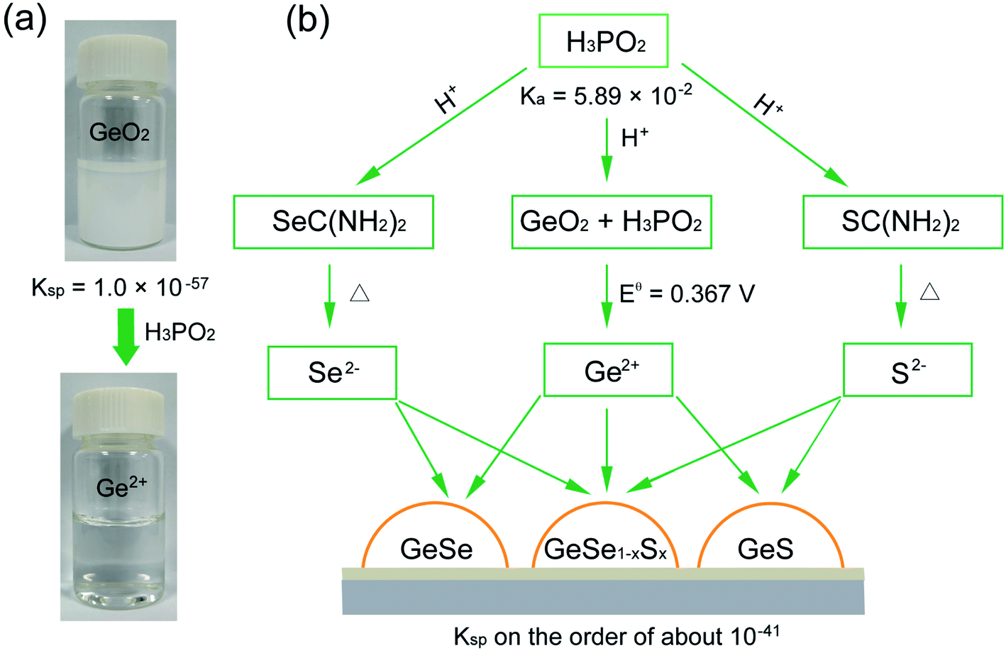 | ||
| Fig. 1 (a) Photographs of GeO2 powder in water before (top) and after (bottom) the addition of H3PO2. (b) Deposition mechanism of Ge(II)-based chalcogenide thin films in the case of GeSe, GeS, and GeSe1−xSx films, where GeO2, thiourea, and selenourea are employed as Ge, S, and Se sources, and H3PO2 is used as a reducing agent and strong acid. | ||
We then pursued an additive agent dissolving the GeO2 powder in water while generating stable Ge2+ in water for the subsequent synthesis of Ge(II)-based chalcogenides. We took the view that this agent would need to meet the following three criteria: (i) this additive should be a suitable reducing agent that reduces insoluble GeO2 into soluble Ge2+ in water; (ii) this additive should be a strong acid that stabilizes Ge2+ in water, since Ge2+ easily hydrolyzes in a weak base or water to form Ge(OH)2;46 (iii) the additive should not be involved in the final deposition of Ge-based chalcogenide thin films.
In this regard, we posited that hypophosphorous acid (H3PO2) may fulfil the above criteria due to its strong acidity with a high dissociation constant (Ka) of 5.89 × 10⁻² and suitable reducibility with a standard electrode potential (Eθ) (H3PO3/H3PO2) of −0.499 V (Fig. 1b).47 We found that H3PO2 readily reduces GeO2 into Ge2+via the following two half reactions:
| H3PO3 + 2H+ + 2e− = H3PO2 + H2O Eθ = −0.499 V |
| GeO2 + 4H+ + 2e− = Ge2+ + 2H2O Eθ = −0.132 V |
The reaction can thereby be written as:
| GeO2 + 2H+ + H3PO2 = Ge2+ + H3PO3 + H2O |
The standard redox potential of this reaction is Eθ = Eθ (GeO2/Ge2+) − Eθ (H3PO3/H3PO2) = 0.367 V (Table S1†), exhibiting negative Gibbs energy ΔrGθ = −nFEθ < 0, where n is the electron transfer number, F is the Faraday constant, and H+ is provided by the dissociation of H3PO2. The pH value of aqueous H3PO2 is measured to be about 0.6. When we added H3PO2 into GeO2 aqueous solution, the milky white solution expectedly becomes colorless and transparent under magnetic stirring at 95 °C for 30 min (Fig. 1a), indicating that insoluble GeO2 has been reduced to soluble and stable Ge2+ in water with the introduction of H3PO2.
We finally introduced commonly used thiourea and selenourea as S and Se sources into this Ge2+ solution (Fig. 1b). This system exhibits a colorless and transparent solution (Fig. S2†), wherein the pH value is measured to be about 0.6 arising from the excessive utility of H3PO2. Thiourea and selenourea would thereby release free S2− and Se2− ions slightly in this strong acid solution, in contrast with thiourea and selenourea in basic solution.48,49 Considering the low Kspvalues of GeS and GeSe in the order of about 10−41,50 free Ge2+ ions would then react with a trace amount of free S2− or Se2− ions to deposit GeS or GeSe on the substrate via a heterogeneous surface reaction, similar to that of the widely-used chemical bath deposition of CdS.38
Fabrication of GeS thin films and their application in photovoltaics
We sought to deposit GeS films onto a substrate of glass coated with fluorine-doped tin oxide (FTO). We transferred the GeO2, H3PO2 and thiourea deposition system into a hydrothermal vessel that was subsequently heated at 160 °C for 4 h (Fig. S3†). We first applied X-ray diffraction (XRD) to characterize the crystal structure of the as-prepared GeS films. Fig. 2a shows the amorphous state of the as-deposited films, indicating that the deposition at 160 °C does not induce crystallization considering the high crystallization temperature of GeS (375 °C).34 The as-deposited amorphous GeS films exhibit a uniform and smooth surface morphology measured from scanning electron microscopy (SEM) characterization (Fig. S4†). Such amorphous GeS films were then subjected to post-annealing at 380 °C for 5 min in a nitrogen atmosphere that led to the formation of orthorhombic GeS (JCPDS 71-0306) (Fig. 2a and S5†). Notably, no phase impurities such as GeS2, GeO2 and Ge are observed from the XRD characterization, despite the utility of GeO2 in the precursor solution. Raman characterization additionally confirms the pure phase of GeS films, where the four peaks correspond to the typical A2g, B21g, A3g, and A4g vibrational modes of GeS (Fig. 2b), respectively, agreeing well with previous reports.51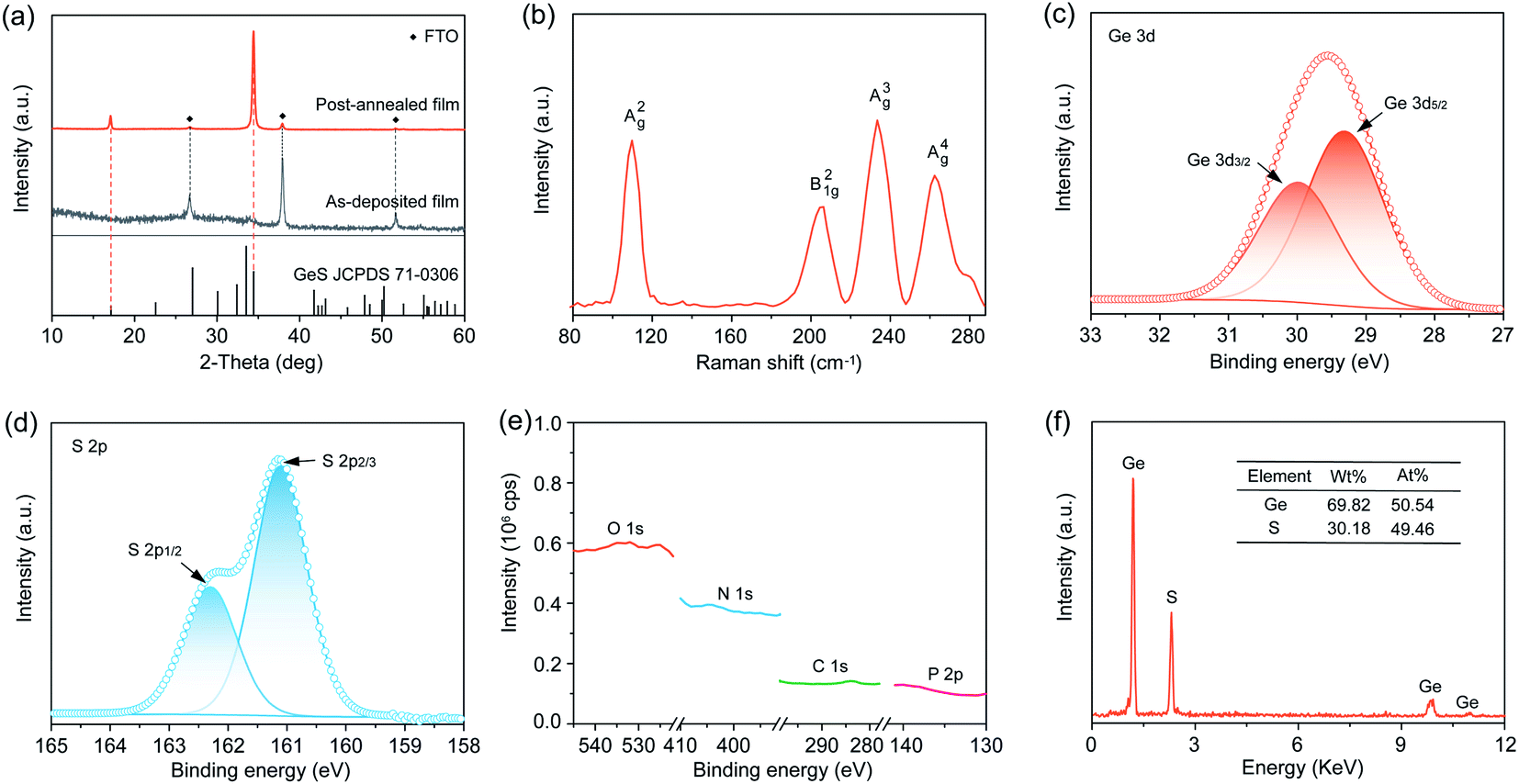 | ||
| Fig. 2 (a) XRD patterns of the as-deposited and subsequently annealed GeS film. (b) Raman spectrum of the GeS film. XPS spectra of (c) Ge 3d, (d) S 2p, and (e) O 1s, N 1s, C 1s and P 2p in the GeS film. (f) EDS spectrum of the GeS film. The inset table represents the composition of the GeS film measured by EDS. | ||
We further applied X-ray photoelectron spectroscopy (XPS) to measure the chemical state of the as-prepared polycrystalline GeS films while checking whether there are any other possible impurities, especially in the amorphous state. The magnified XPS spectrum of Ge exhibits a 3d doublet with fitting at binding energies of 29.42 (3d5/2) and 30.0 eV (3d3/2) (Fig. 2c), in good agreement with the expected binding energy in GeS.34 No other possible Ge chemical states such as Ge4+ in GeS2 and GeO2 are found in the XPS spectrum considering the perfect Gaussian–Lorentzian peak fitting of Ge 3d. Similarly, S exhibits the expected valence state of S2− in GeS (Fig. 2d), indicating the high purity of solution-processed GeS films. High-resolution scan especially on P (2p), O (1s), N (1s), and C (1s) demonstrates that no detectable P, O, N, and C are present in the as-prepared GeS films (Fig. 2e and S6†), despite the utility of H3PO2, GeO2, and thiourea. Energy dispersive X-ray spectroscopy (EDS) was carried out to investigate the chemical composition of the GeS films. The Ge![[thin space (1/6-em)]](https://www.rsc.org/images/entities/char_2009.gif) :S atomic ratio is nearly 1:1 (Fig. 2f), matching well with the stoichiometry of GeS. In brief, the above material characterization results gathered from XRD, Raman spectroscopy, XPS, and EDS confirm that the solution-processed films are pure GeS without any impurities of GeS2, GeO2, or Ge, thereby indicating that our design strategy of solution-processed Ge(II)-based chalcogenide films is effective at excluding impurity contamination especially for Ge(IV).
:S atomic ratio is nearly 1:1 (Fig. 2f), matching well with the stoichiometry of GeS. In brief, the above material characterization results gathered from XRD, Raman spectroscopy, XPS, and EDS confirm that the solution-processed films are pure GeS without any impurities of GeS2, GeO2, or Ge, thereby indicating that our design strategy of solution-processed Ge(II)-based chalcogenide films is effective at excluding impurity contamination especially for Ge(IV).
We then performed top-view and cross-sectional SEM as well as atomic force microscopy (AFM) to characterize the morphology and thickness of the as-fabricated polycrystalline GeS films. These films show a compact surface morphology with the grain size close to 300 nm (Fig. 3a). AFM analysis shows that the as-prepared GeS films are smooth with a root-mean square roughness of 35.6 nm (Fig. S7a†). The thickness of the GeS film is directly measured to be around 500 nm (Fig. 3b), which is thick enough to absorb much of the incident sunlight due to the large absorption coefficient of GeS (greater than 105 cm−1).34 The thickness of GeS films can be easily regulated by varying the deposition time, where the 1.5 h, 3 h and 6 h deposition processes lead to an increased thickness from 212 nm through 463 nm to 765 nm, respectively (Fig. S8†). Optical properties of such solution-processed GeS films were characterized by absorption spectroscopy. The absorption of GeS films decreases sharply at a wavelength of about 600 nm, and gradually drops to almost zero at a wavelength longer than 800 nm (Fig. 3c). The wavelength-dependent absorption coefficient is then calculated via the Beer–Lambert law, which is higher than 105 cm−1 at a wavelength shorter than 600 nm (Fig. 3d). The bandgap of GeS films is further calculated to be 1.71 eV by plotting (αhν)1/2versus (hν). The above optical results are consistent with the previous reports based on GeS,52,53 further demonstrating the pure-phase of our solution-processed GeS films.
 | ||
| Fig. 3 (a) Top-view and (b) cross-sectional SEM images of GeS films deposited on top of FTO substrates. (c) Absorption spectrum of the GeS film. (d) Wavelength-dependent absorption coefficient of the GeS film. Inset: Tauc plot for the GeS film. (e) Schematic of the solution-processed GeS solar cell. (f) J–V curves of the GeS solar cell in the dark and under 100 mW cm−2 simulated AM 1.5G irradiation, respectively. | ||
To explore the suitability of our solution-processed GeS films for photovoltaic applications, we employed the resulting polycrystalline GeS film as the active layer to construct heterojunction solar cells with a structure of glass/FTO/GeS/CdS/i-ZnO/ITO/Ag (Fig. 3e). Fig. 3f shows the current density versus voltage (J–V) characteristics of the device measured under the standard AM 1.5G illumination at an intensity of 100 mW cm−2 and in the dark. The best device exhibits a power conversion efficiency of 0.8%, with an open-circuit voltage (Voc) of 0.52 V, a short-circuit current density (Jsc) of 4.9 mA cm−2, and a fill factor (FF) of 31%. In this GeS solar cell, the Voc deficit with respect to its bandgap of 1.7 eV (Eg/q − Voc) is as high as 1.18 V, which possibly originated from the high defect density at the GeS/CdS heterojunction interface. The low Jsc may be mainly attributed to the [100]-oriented grain in the as-prepared polycrystalline GeS film as evidenced in Fig. 2a, where the carriers are required to hop between layers held by weak van der Waals forces. Furthermore, the small grain size of GeS could bring extra grain boundaries in the polycrystalline film, which may act as carrier recombination centers, resulting in severe carrier recombination loss and then low Jsc. The GeS device is also limited by a low FF of 31%, which is most likely due to the poor GeS/CdS heterojunction interface and the less optimized sputtering process of i-ZnO and ITO. Therefore, the device performance could be boosted by passivating GeS/CdS interfacial defects, optimizing the deposition process to obtain a large grain size of GeS, regulating the film growth orientation to achieve the [010]/[001] orientation that enables the carrier transport within the covalently bonded Ge–S layers, and introducing a hole transport layer to improve the carrier collection efficiency. Although this preliminary device efficiency is quite low, this is the first solution-processed GeS solar cell reported so far, and the result is still encouraging that fully demonstrates the great potential of our solution-processed GeS films for photovoltaic applications.
Fabrication of GeSe1−xSx alloy thin films
To further extend the utility of our H3PO2-based solution processing of Ge(II) chalcogenide thin films, we sought to deposit GeSe1−xSx alloy thin films across the entire compositional range from x = 0 to 1 by mixing thiourea and selenourea with different ratios in the precursor solution to adjust the S/Se atomic ratio in the final films. Very recently, Huang et al. reported the fabrication of high-quality GeSe1−xSx alloy flakes via chemical vapor transport, demonstrating the great potential of GeSe1−xSx alloys for continuously tunable optoelectronic applications.32 In contrast with the vapor-assisted approaches, which may be limited to intolerable stoichiometric deviation, the solution process enables the precise control of the stoichiometry predetermined by the composition of the starting precursors in solution.We employed XRD to characterize the formation of the GeSe1−xSx alloy phase when adding different amounts of selenourea into the Ge–S precursor solution. Fig. 4a shows the XRD patterns of four different as-deposited films produced using thiourea and selenourea with S/(S + Se) ratios of 0.7, 0.5, 0.3, and 0, followed by a thermal annealing step at 380 °C for 5 min in a nitrogen atmosphere. All four films crystallize into the orthorhombic structure with no additional and split diffraction peaks, demonstrating the formation of pure-phase GeSe1−xSx alloys without any secondary phases or impurities. The variation of the S/(S + Se) ratio in the as-deposited GeSe1−xSx films is clearly demonstrated in the XRD patterns. When decreasing the S content, a gradual shift to a smaller 2θ angle is observed in the magnified view of (400) peaks (Fig. 4b), where the peaks of the FTO substrate remain constant. Such a shift to lower angles is attributed to the increased lattice constants of the films with gradual substitution of smaller S atoms (1.84 Å) with larger Se atoms (1.98 Å).10 At x = 0, the XRD pattern corresponds to orthorhombic GeSe (JCPDS 48-1226). We then obtained the S concentration (x = 0.75, 0.44, 0.28, and 0) via Vegard's law through the calculated lattice parameters deduced from the XRD results (Fig. 4c). We further applied EDS to verify the S/Se composition more precisely. The S/Se atom ratio measured directly from EDS agrees well with the results obtained from XRD patterns (Table S2†), further confirming the composition of the as-deposited films as GeSe1−xSx alloy films.
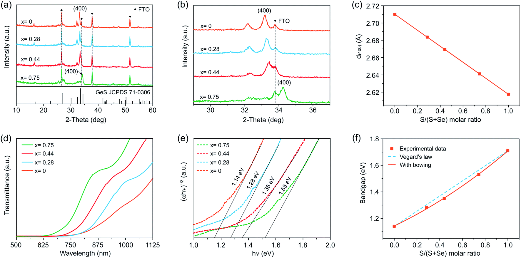 | ||
| Fig. 4 (a) XRD patterns of GeSe1−xSx films with different thiourea/selenourea ratios. (b) Enlarged (400) XRD peaks of the same films as in panel a. (c) (400) d-spacing derived from XRD diffraction peaks, plotted as a function of S concentration x in GeSe1−xSx alloy films. (d) Transmittance spectra of GeSe1−xSx alloy films. (e) Plots of (αhν)1/2versus hν for GeSe1−xSx alloy films. (f) Plot of the bandgap versus S concentration x in GeSe1−xSx alloy films. The solid curve is a quadratic fit to the measured values of the bandgap. | ||
We further applied SEM to characterize the morphologies of such GeSe1−xSx films. Only the as-prepared GeSe film shows a compact and smooth surface morphology with a root-mean square roughness of 55.9 nm (Fig. S7b and S9†). We then fabricated GeSe thin-film solar cells using the architecture of FTO/CdS/GeSe/Au (Fig. S10†). The champion device shows an efficiency of 0.77% under 100 mW cm−2 simulated AM 1.5G irradiation, with a Voc of 0.2 V, a Jsc of 9.1 mA cm−2, and a FF of 42%, the first solution-processed GeSe solar cells. However, all alloy films of GeSe0.25S0.75, GeSe0.56S0.44, and GeSe0.72S0.28 exhibit apparent pinholes and cracks (Fig. S11†), which cannot be directly used to fabricate thin-film solar cells. This may be attributed to the different reactivities of S and Se precursors. The quality of alloy films should be further improved by exploring suitable S and Se precursors.
We finally carried out transmission spectroscopy to determine the optical bandgaps of these GeSe1−xSx alloy films. There is a continuous red shift in transmission spectra with increased Se composition arising from the narrower bandgap of GeSe than that of GeS (Fig. 4d). The bandgaps of the four films estimated by plotting (αhν)1/2versus (hν) are found to be 1.53, 1.35, 1.28, and 1.14 eV for x = 0.75, 0.44, 0.28, and 0, respectively (Fig. 4e). Combined with 1.71 eV for GeS, the bandgaps of our solution-processed GeSe1−xSx alloy films cover the entire range from 1.71 eV for GeS to 1.14 eV for GeSe. To further investigate the relation between the alloy composition and corresponding bandgap evolution, we first plotted the bandgaps of GeSe1−xSx alloy films as a function of S concentration x via Vegard's law of Eg(GeSe1−xSx) = (1 − x)Eg(GeSe) + xEg(GeS) (Fig. 4f), which empirically describes the linear relation between the composition and bandgaps.10 It is obvious that the bandgap values deviate from the linear trend that is fairly common and is widely exhibited for other ternary and quaternary compounds.11,54 We further assessed the deviation from the linear trend through adding a nonlinear (bowing) term to Vegard's law written as Eg(GeSe1−xSx) = (1 − x)Eg(GeSe) + xEg(GeS) − bx(1 − x). The dependence of bandgaps on S concentration x is then characterized by the relation Eg (x) = 0.15x2 + 0.41x + 1.14 eV, wherein the bowing parameter of the GeSe1−xSx alloy films is determined to be 0.15. Such a nonlinear dependence of the bandgap on the S concentration may be attributed to the change of the band structure due to the lattice constant variation and electron distribution deformation arising from the electronegativity differences of the alloy films.10
Conclusions
In summary, we report solution-processed fabrication of Ge(II)-based chalcogenide thin films in the case of GeS and GeSe films. This is achieved via the introduction of H3PO2 that enables the formation of Ge(II) ions from low-cost and stable GeO2 powder while suppressing the oxidation of Ge(II) to Ge(IV) in precursor solution. High-quality GeS films with no Ge(IV) phase impurity and P, O, N and C contamination were successfully obtained. Solar cells based on these solution-processed GeS films exhibited an efficiency of 0.8%, the first observed photovoltaic effect in a solution-processed GeS film device. Furthermore, GeSe1−xSx alloy films with continuously tunable bandgaps ranging from 1.71 (GeS) to 1.14 eV (GeSe) were processed by simply adjusting the atomic ratio of S- to Se-precursors in solution, indicating the great potential of this H3PO2-based solution processing for the fabrication of Ge(II) chalcogenide thin films.Data availability
All available data are included in ESI.†Author contributions
The manuscript was written through contributions of all authors. All authors have given approval to the final version of the manuscript.Conflicts of interest
The authors declare no competing financial interest.Acknowledgements
This work was supported by the National Natural Science Foundation of China (21922512 and 21875264), the Youth Innovation Promotion Association CAS (Y2021014) and the Graduate Student Innovation Project of Shanxi Province (2020SY336).References
- F. P. García de Arquer, D. V. Talapin, V. I. Klimov, Y. Arakawa, M. Bayer and E. H. Sargent, Science, 2021, 373, eaaz8541 CrossRef PubMed.
- R. Tang, X. Wang, W. Lian, J. Huang, Q. Wei, M. Huang, Y. Yin, C. Jiang, S. Yang, G. Xing, S. Chen, C. Zhu, X. Hao, M. A. Green and T. Chen, Nat. Energy, 2020, 5, 587–595 CrossRef CAS.
- M. Graetzel, R. A. J. Janssen, D. B. Mitzi and E. H. Sargent, Nature, 2012, 488, 304–312 CrossRef CAS PubMed.
- C. N. Bucherl, K. R. Oleson and H. W. Hillhouse, Curr. Opin. Chem. Eng., 2013, 2, 168–177 CrossRef.
- Z. Li, T. R. Klein, D. H. Kim, M. Yang, J. J. Berry, M. F. van Hest and K. Zhu, Nat. Rev. Mater., 2018, 3, 18017 CrossRef CAS.
- M. V. Kovalenko, Nat. Nanotechnol., 2015, 10, 994–997 CrossRef CAS PubMed.
- C. R. Kagan, E. Lifshitz, E. H. Sargent and D. V. Talapin, Science, 2016, 353, aac5523 CrossRef PubMed.
- Y. Deng, S. Xu, S. Chen, X. Xiao, J. Zhao and J. Huang, Nat. Energy, 2021, 6, 633–641 CrossRef CAS.
- X. Wang, R. Tang, C. Jiang, W. Lian, H. Ju, G. Jiang, Z. Li, C. Zhu and T. Chen, Adv. Energy Mater., 2020, 10, 2002341 CrossRef CAS.
- Z. Xia, J. Zhong, M. Leng, L. Hu, D.-J. Xue, B. Yang, Y. Zhou, X. Liu, S. Qin, Y.-B. Cheng and J. Tang, Chem. Mater., 2015, 27, 8048–8057 CrossRef CAS.
- Z. Lin, Q. He, A. Yin, Y. Xu, C. Wang, M. Ding, H.-C. Cheng, B. Papandrea, Y. Huang and X. Duan, ACS Nano, 2015, 9, 4398–4405 CrossRef CAS PubMed.
- H. Zhang, J. S. Son, D. S. Dolzhnikov, A. S. Filatov, A. Hazarika, Y. Wang, M. H. Hudson, C.-J. Sun, S. Chattopadhyay and D. V. Talapin, Chem. Mater., 2017, 29, 6396–6404 CrossRef CAS.
- C. Jiang, J. Zhou, R. Tang, W. Lian, X. Wang, X. Lei, H. Zeng, C. Zhu, W. Tang and T. Chen, Energy Environ. Sci., 2021, 14, 359–364 RSC.
- B. Bob, B. Lei, C.-H. Chung, W. Yang, W.-C. Hsu, H.-S. Duan, W. W.-J. Hou, S.-H. Li and Y. Yang, Adv. Energy Mater., 2012, 2, 504–522 CrossRef CAS.
- E. H. Sargent, Nat. Photonics, 2012, 6, 133–135 CrossRef CAS.
- J. Kim, H. Hiroi, T. K. Todorov, O. Gunawan, M. Kuwahara, T. Gokmen, D. Nair, M. Hopstaken, B. Shin, Y. S. Lee, W. Wang, H. Sugimoto and D. B. Mitzi, Adv. Mater., 2014, 26, 7427–7431 CrossRef CAS PubMed.
- D. H. Webber and R. L. Brutchey, J. Am. Chem. Soc., 2013, 135, 15722–15725 CrossRef CAS PubMed.
- D. V. Talapin, J.-S. Lee, M. V. Kovalenko and E. V. Shevchenko, Chem. Rev., 2010, 110, 389–458 CrossRef CAS PubMed.
- P. D. Antunez, D. A. Torelli, F. Yang, F. A. Rabuffetti, N. S. Lewis and R. L. Brutchey, Chem. Mater., 2014, 26, 5444–5446 CrossRef CAS.
- C. L. McCarthy, D. H. Webber, E. C. Schueller and R. L. Brutchey, Angew. Chem., Int. Ed., 2015, 127, 8498–8501 CrossRef.
- D. B. Mitzi, M. Yuan, W. Liu, A. J. Kellock, S. J. Chey, V. Deline and A. G. Schrott, Adv. Mater., 2008, 20, 3657–3662 CrossRef CAS.
- M. Yuan and D. B. Mitzi, Dalton Trans., 2009, 6078–6088 RSC.
- C.-J. Hsu, H.-S. Duan, W. Yang, H. Zhou and Y. Yang, Adv. Energy Mater., 2013, 4, 1301287 CrossRef.
- H.-S. Duan, W. Yang, B. Bob, C.-J. Hsu, B. Lei and Y. Yang, Adv. Funct. Mater., 2012, 23, 1466–1471 CrossRef.
- A. Walsh, S. Chen, S.-H. Wei and X.-G. Gong, Adv. Energy Mater., 2012, 2, 400–409 CrossRef CAS.
- S. Chen, A. Walsh, X. G. Gong and S. H. Wei, Adv. Mater., 2013, 25, 1522–1539 CrossRef CAS PubMed.
- X. Zhou, Q. Zhang, L. Gan, H. Li, J. Xiong and T. Zhai, Adv. Sci., 2016, 3, 1600177 CrossRef PubMed.
- X. Wang, Y. Li, L. Huang, X.-W. Jiang, L. Jiang, H. Dong, Z. Wei, J. Li and W. Hu, J. Am. Chem. Soc., 2017, 139, 14976–14982 CrossRef CAS PubMed.
- X. Zhou, X. Hu, B. Jin, J. Yu, K. Liu, H. Li and T. Zhai, Adv. Sci., 2018, 5, 1800478 CrossRef PubMed.
- S.-C. Liu, Z. Li, J. Wu, X. Zhang, M. Feng, D.-J. Xue and J.-S. Hu, Sci. China Mater., 2021, 64, 2118–2126 CrossRef CAS.
- Y. Ye, Q. Guo, X. Liu, C. Liu, J. Wang, Y. Liu and J. Qiu, Chem. Mater., 2017, 29, 8361–8368 CrossRef CAS.
- S. Liu, Q. Ma, C. Lin, C. Hong, R. Yi, R. Wang, R. Li, X. Liu, A. Nie, X. Gan, Y. Cheng and W. Huang, Phys. Rev. Mater., 2020, 4, 074012 CrossRef CAS.
- S.-C. Liu, C.-M. Dai, Y. Min, Y. Hou, A. H. Proppe, Y. Zhou, C. Chen, S. Chen, J. Tang, D.-J. Xue, E. H. Sargent and J.-S. Hu, Nat. Commun., 2021, 12, 670 CrossRef CAS PubMed.
- M. Feng, S.-C. Liu, L. Hu, J. Wu, X. Liu, D.-J. Xue, J.-S. Hu and L.-J. Wan, J. Am. Chem. Soc., 2021, 143, 9664–9671 CrossRef CAS PubMed.
- K. Li, X. Lin, B. Song, R. Kondrotas, C. Wang, Y. Lu, X. Yang, C. Chen and J. Tang, Front. Optoelectron., 2021, 14, 482–490 CrossRef.
- C. Wang, X. Du, S. Wang, H. Deng, C. Chen, G. Niu, J. Pang, K. Li, S. Lu, X. Lin, H. Song and J. Tang, Front. Optoelectron., 2021, 14, 341–351 CrossRef.
- S.-C. Liu, Y. Yang, Z. Li, D.-J. Xue and J.-S. Hu, Mater. Chem. Front., 2020, 4, 775–787 RSC.
- D.-J. Xue, S.-C. Liu, C.-M. Dai, S. Chen, C. He, L. Zhao, J.-S. Hu and L.-J. Wan, J. Am. Chem. Soc., 2017, 139, 958–965 CrossRef CAS PubMed.
- D. B. Mitzi, Inorg. Chem., 2005, 44, 3755–3761 CrossRef CAS PubMed.
- D. J. Milliron, S. Raoux, R. M. Shelby and J. Jordan-Sweet, Nat. Mater., 2007, 6, 352–356 CrossRef CAS PubMed.
- G. M. Ford, Q. Guo, R. Agrawal and H. W. Hillhouse, Chem. Mater., 2011, 23, 2626–2629 CrossRef CAS.
- T. Krishnamoorthy, H. Ding, C. Yan, W. L. Leong, T. Baikie, Z. Zhang, M. Sherburne, S. Li, M. Asta, N. Mathews and S. G. Mhaisalkar, J. Mater. Chem. A, 2015, 3, 23829–23832 RSC.
- C. C. Stoumpos, L. Frazer, D. J. Clark, Y. S. Kim, S. H. Rhim, A. J. Freeman, J. B. Ketterson, J. I. Jang and M. G. Kanatzidis, J. Am. Chem. Soc., 2015, 137, 6804–6819 CrossRef CAS PubMed.
- O. A. Babich, M. C. Ghosh and E. S. Gould, Chem. Commun., 2000, 907–908 RSC.
- Z. Xiao, X. Sun, X. Li, Y. Wang, Z. Wang, B. Zhang, X. L. Li, Z. Shen, L. B. Kong and Y. Huang, Nano Lett., 2018, 18, 3290–3296 CrossRef CAS PubMed.
- W. Sun, G. Zhong, C. Kübel, A. A. Jelle, C. Qian, L. Wang, M. Ebrahimi, L. M. Reyes, A. S. Helmy and G. A. Ozin, Angew. Chem., Int. Ed., 2017, 56, 6329–6334 CrossRef CAS PubMed.
- J. G. Speight, Lange's Handbook of Chemistry, McGraw-Hill, New York, 2005 Search PubMed.
- A.-U. Rahman, M. A. Medrano and B. E. Jeanneret, J. Org. Chem., 1962, 27, 3315–3317 CrossRef CAS.
- A. U. Rahman, M. A. Medrano and O. P. Mittal, Recl. Trav. Chim., 1960, 79, 188–192 CrossRef CAS.
- S. Licht, J. Electrochem. Soc., 1988, 135, 2971–2975 CrossRef CAS.
- H. B. Ribeiro, S. L. L. M. Ramos, L. Seixas, C. J. S. de Matos and M. A. Pimenta, Phys. Rev. B, 2019, 100, 094301 CrossRef CAS.
- C.-H. Ho and J.-X. Li, Adv. Opt. Mater., 2017, 5, 1600814 CrossRef.
- S. U. Rehman, F. K. Butt, Z. Tariq, B. Ul. Haq, G. Lin and C. Li, Sol. Energy, 2019, 185, 211–221 CrossRef.
- J. Wu, S.-C. Liu, Z. Li, S. Wang, D.-J. Xue, Y. Lin and J.-S. Hu, Natl. Sci. Rev., 2021, 8, nwab047 CrossRef CAS PubMed.
Footnotes |
| † Electronic supplementary information (ESI) available. See https://doi.org/10.1039/d1sc07043f |
| ‡ These authors contributed equally. |
| This journal is © The Royal Society of Chemistry 2022 |