
 Open Access Article
 This Open Access Article is licensed under a Creative Commons Attribution-Non Commercial 3.0 Unported Licence
Defect engineering in semiconductor-based SERS
Ge
Song
ab,
Shan
Cong
 acd and
Zhigang
Zhao
*abc
acd and
Zhigang
Zhao
*abc
aSchool of Nano-Tech and Nano-Bionics, University of Science and Technology of China, Hefei 230026, China
bKey Lab of Nanodevices and Applications, Suzhou Institute of Nano-Tech and Nano-Bionics, Chinese Academy of Sciences, Suzhou 215123, China. E-mail: zgzhao2011@sinano.ac.cn
cKey Laboratory of Multifunctional Nanomaterials and Smart Systems, Chinese Academy of Sciences (CAS), Suzhou 215123, China
dGusu Laboratory of Materials, Suzhou 215123, China
First published on 1st December 2021
Abstract
Semiconductor-based surface enhanced Raman spectroscopy (SERS) platforms take advantage of the multifaceted tunability of semiconductor materials to realize specialized sensing demands in a wide range of applications. However, until quite recently, semiconductor-based SERS materials have generally exhibited low activity compared to conventional noble metal substrates, with enhancement factors (EF) typically reaching 103, confining the study of semiconductor-based SERS to purely academic settings. In recent years, defect engineering has been proposed to effectively improve the SERS activity of semiconductor materials. Defective semiconductors can now achieve noble-metal-comparable SERS enhancement and exceedingly low, nano-molar detection concentrations towards certain molecules. The reason for such success is that defect engineering effectively harnesses the complex enhancement mechanisms behind the SERS phenomenon by purposefully tailoring many physicochemical parameters of semiconductors. In this perspective, we introduce the main defect engineering approaches used in SERS-activation, and discuss in depth the electromagnetic and chemical enhancement mechanisms (EM and CM, respectively) that are influenced by these defect engineering methods. We also introduce the applications that have been reported for defective semiconductor-based SERS platforms. With this perspective we aim to meet the imperative demand for a summary on the recent developments of SERS material design based on defect engineering of semiconductors, and highlight the attractive research and application prospects for semiconductor-based SERS.
 Ge Song | Ge Song obtained her BSc in Chemistry from China Agricultural University and an MSc in Chemistry from Bristol University. She is now a PhD student at the University of Science and Technology China. Her research interests are inorganic nanomaterials and their SERS activities. |
 Shan Cong | Shan Cong is a Professor at Suzhou Institute of Nanotech and Nanobionics, CAS, and a member of the Youth Innovation Promotion Association, CAS. He received his PhD from Zhejiang University in 2011. His research interests include the synthesis of low-dimensional nanocrystals and their applications in surface-enhanced Raman scattering (SERS) and photocatalysis. |
 Zhigang Zhao | Zhigang Zhao is a Professor at Suzhou Institute of Nanotech and Nanobionics, Chinese Academy of Sciences. He received his PhD from Institute of Metal Research, Chinese Academy of Sciences in 2006, and did postdoctoral research at Dayton University (USA), Osaka University (Japan) and the National Institute of Advanced Industrial Science and Technology (AIST, Japan) from 2006 to 2011. His research interests include novel surface-enhanced Raman spectroscopy (SERS)-active materials and their applications. |
1. Introduction
SERS is an analytical tool used for obtaining fingerprint chemical information of a given surface via Raman spectroscopy. The non-destructive, ultrasensitive and generally rapid features afforded by the technique have attracted wide interest in the fields of materials, catalysis, biology and medicine. Conventionally, noble metal materials such as Au and Ag nanoparticles have been widely applied in SERS research. Noble metal nanoparticles, which exhibit inherently prominent localized surface plasmonic resonance (LSPR) activity, are often assembled into arrays to further induce strong EM enhancement, and have been used in the detection of probe molecules such as DNA structures, pesticide residues and small organic molecules.1–6 However, noble metal-based substrates have also met challenges, such as high cost, difficulty of mass production, instability, and lack of selectivity.7 As a relatively new branch of SERS research, semiconductors have been speculated as ideal SERS materials due to their multifaceted tunability, wide variety and easy accessibility.8–24 It is speculated that semiconductor-based SERS substrates may complement noble metals by allowing for a wider selection of SERS-active materials, improved selectivity to probe molecules and reproducible mass production of SERS substrates. Based on the tuning of the band structure, selective interfacial interactions and signal enhancement can be produced towards specific probe molecules, while the tuning of surface properties and density of states (DOS) can result in more effective and reliable enhancement. These properties make semiconductors potentially valuable in the construction of specialized SERS platforms. However, due to the relative complexity of principles responsible for semiconductor-based SERS phenomena, the activation of SERS in semiconductors has for a long time been a great challenge. For this reason, strategies for designing highly SERS-active semiconductor substrates are urgently needed.Defect engineering, which has long been well-established in the study of semiconductor materials, provides a series of ubiquitously effective strategies for activating and boosting the innate SERS activity of semiconductors. Defect engineering comprises a series of techniques that purposefully aim to break the periodic arrangement of atoms, and can be loosely divided into point defects and disorders of higher dimensions. Generally, they alter the band structure, surface properties and density of states of semiconductors, endowing semiconductors with enhanced light-trapping ability, surface interactions or charge-transport efficiency, which directly influence the SERS effect. Charge transfer (CT) processes, which are a dominant aspect of CM principles behind semiconductor-based SERS, directly benefit from the defect-induced physicochemical changes to semiconductors, thereby making defect engineering widely applicable and highly versatile for semiconductor-based SERS. As a result of recent research efforts, a myriad of SERS-active semiconductor substrates have emerged, which have creatively exploited defect engineering techniques, broadening the insight into defect engineering and mechanisms behind SERS. In addition to fundamental research interest, sensitive and selective SERS responses towards analyte species ranging from inorganic molecules to large molecular superstructures have been obtained, with presently reported EF reaching 108,25 showing great promise for the practical application of semiconductor-based SERS.
This perspective targets the imperative need for a systematic summary of the rational design of defective semiconductors that have emerged over recent years, which encompass several major categories of materials including metal oxides, nitrides, transition metal dichalcogenides (TMDs) and carbon materials. Furthermore, the linkage of various defects to SERS activity is discussed by identifying the three main material parameters that are affected by defect engineering, namely, the band structure, surface active sites and DOS (Scheme 1). The applications of such defective semiconductors as SERS platforms are also introduced, stretching across multiple disciplines such as trace sensing for food and environmental safety, biological sensing, reaction monitoring and CT characterization in chemical cells. The aim is to elucidate recent developments in the mechanistic principles of SERS, and defect engineering strategies available to researchers, in the hope that fellow researchers may be well-equipped in the search for SERS-activating strategies and deploying semiconductor-based SERS platforms in real-world applications.
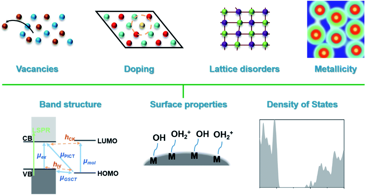 | ||
| Scheme 1 Depiction of the main categories of defects in SERS-active semiconductors and material parameters that are influenced by defect engineering. | ||
2. Defect engineering strategies for SERS-active semiconductors
In this section the types of defects and their influences on the SERS activity of semiconductors are discussed. The classification of defects is usually based on the dimensionality of defects. Here, we examine the four types of defects most relevant to current research on the engineering of SERS-active semiconductors. However, it is worth noting that research into defect engineering extends far beyond these four categories, and there is yet much to be understood about the relationship between different defective structures and the chemical enhancement processes responsible for SERS activity. A summary of all materials discussed in this section is presented in Table 1.| Defect types | Materials | Molecules | Reported SERS performance | Ref. | |
|---|---|---|---|---|---|
| EF | LOD | ||||
| Vacancies | H2/Ar-W18O49 | R6G | 3.4 × 10⁵ | 1 × 10⁻⁷ mol L−1 | 26 |
| Cu2O | 4-MPY | 5 × 10⁻¹⁰ mol L−1 | 27 | ||
| WO3−x | R6G | 1.1 × 10⁴ | 1 × 10⁻⁷ mol L−1 | 31 | |
| ZnO1−x | R6G | 1.1 × 10⁴ | 1 × 10⁻⁷ mol L−1 | 31 | |
| WO3 | Au-4MBA | 10.00 | 32 | ||
| Au/TiO2 | DNT | 1 × 10⁻¹⁵ mol L−1 | 33 | ||
| Ag/Ag–TiO2 | 4-MBA | 1.68 × 10⁶ | 35 | ||
| WO3 | RhB | 1.14 × 10⁶ | 1 × 10⁻⁷ mol L−1 | 36 | |
| TiO2 | PABA | 1 × 10⁻⁸ mol L−1 | 37 | ||
| Cu2O | SR3 | 0.3 mg kg−1 | 40 | ||
| MoS2 | R6G | 63.5 | 41 | ||
| Dopants | TiO2–xNy | R6G | 5 × 10⁻⁸ mol L−1 | 31 | |
| Black TiO2 | R6G | 1.2 × 10⁶ | 1 × 10⁻⁷ mol L−1 | 42 | |
| Cation-intercalated WO3 | R6G | 8.86 × 10⁴ | 1 × 10⁻⁶ mol L−1 | 43 | |
| Co–MoO3−x | MB | 1.01 × 10⁵ | 1 × 10⁻⁷ mol L−1 | 48 | |
| N-doped graphene | RhB | 5 × 10⁻¹¹ mol L−1 | 61 | ||
| N-doped graphite | CV | 3.2 × 10⁷ | 1 × 10⁻⁷ mol L−1 | 62 | |
| Ozone-treated graphene | RhB | 2.5 × 10⁴ | 57 | ||
| MoS2−xOx | R6G | 1.4 × 10⁵ | 1 × 10⁻⁷ mol L−1 | 63 | |
| Lattice disorders | Amorphous TiO2 nanosheets | 4-MBA | 1.86 × 10⁶ | 64 | |
| Amorphous ZnO nanocages | 4-MBA | 6.62 × 10⁵ | 65 | ||
| Amorphous Rh3S6 | 4-NBT | 3 × 10⁴ | 1 × 10⁻⁷ mol L−1 | 66 | |
| R6G | 1 × 10⁵ | ||||
| HxMoO3 quantum dots | MB | 9.5 × 10⁵ | 1 × 10⁻⁹ mol L−1 | 67 | |
| Ni(OH)2 | MB | 2.35 × 10³ | 1 × 10⁻⁸ mol L−1 | 68 | |
| Ultrathin WO3 nanosheets | MB | 1 × 10⁻⁷ mol L−1 | 69 | ||
| Cu2O superstructures | R6G | 8 × 10⁵ | 6 × 10⁻⁹ mol L−1 | 38 | |
| Defective VO2 nanosheets | R6G | 1 × 10⁻⁷ mol L−1 | 71 | ||
| h-MoO3 | MB | 6.99 × 10⁵ | 1 × 10⁻⁹ mol L−1 | 72 | |
| Metallicity | MoO2 | R6G | 3.75 × 10⁶ | 1 × 10⁻⁷ mol L−1 | 74 |
| MoO2−x | R6G | 1 × 10⁻⁸ mol L−1 | 75 | ||
| δ-MoN | R6G | 8.16 × 10⁶ | 1 × 10⁻¹⁰ mol L−1 | 76 | |
| γ-Mo2N | 2,4,5-TCP, 2,4-DCP | 1 × 10⁻¹¹ mol L−1 | 77 | ||
| δ-MoN | R6G | 3.6 × 10⁷ | 1 × 10⁻¹¹ mol L−1 | 78 | |
| VO2 | R6G | 6.7 × 10⁷ | 1 × 10⁻¹⁰ mol L−1 | 79 | |
| TiN | R6G | ∼105 | 1 × 10⁻⁷ mol L−1 | 80 | |
| Ti3O5 | R6G | 1 × 10⁻¹⁰ mol L−1 | 81 | ||
2.1 Vacancies
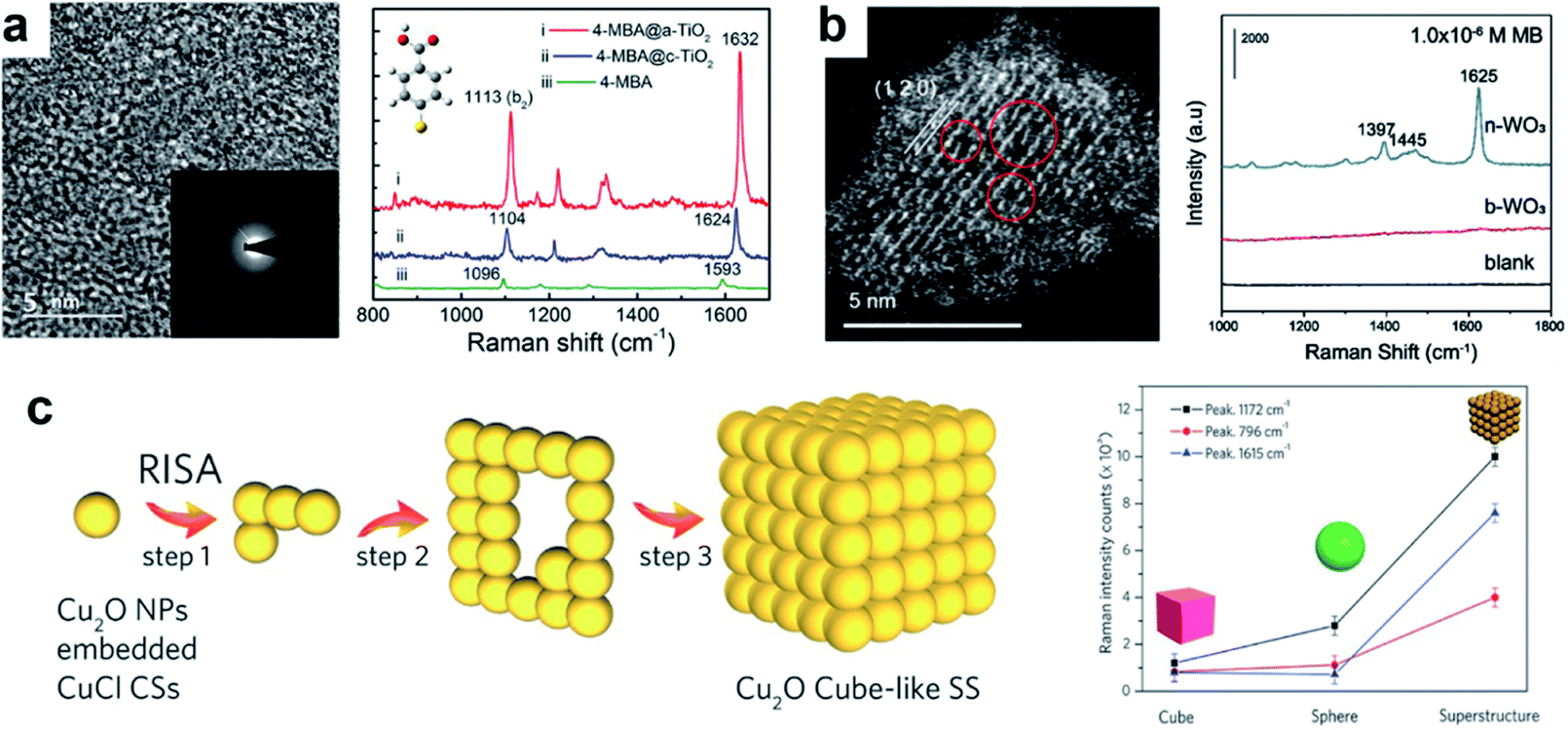
Vacancies, the most well-studied type of defect in semiconductors, result from missing atoms in a crystal lattice. Although both metal and anionic vacancies can occur simultaneously in order to balance the charge within the lattice, nevertheless the types of vacancies are herein identified by their predominant occurrence, based on the final stoichiometry of the defective material as compared with that of its pristine counterpart.Oxygen vacancies (OVs) are among the most prominently studied types of defects in SERS active materials, and oxygen-deficient metal oxides have been widely reported in recent years to exhibit SERS activity where their pristine forms are nearly inert. OVs are easily introduced into metal oxides by post-synthesis treatment means. Cong et al. for the first time reported achieving noble-metal-comparable SERS performance towards R6G by producing surface oxygen vacancies in W18O49 through H2 or Ar atmosphere annealing (Fig. 1a).26 It was proposed that the OVs play an irreplaceable role in magnifying the substrate–molecule surface interaction and promoting CT at the interface. Following this, thermal treatment has also been found effective in inducing OV-related SERS in other typical metal oxides. Yang et al.27 proposed the fabrication of Cu2O octahedrons with oxygen-vacancies by calcining Cu-MOFs in a reductive atmosphere, which facilitated stronger selective adsorption towards sulfhydryl groups, achieving an LOD of 5 × 10⁻¹⁰ M for 4-MPY. In addition to thermal treatment, irradiation-induced vacancies are also widely reported in materials engineering.28–30 Zheng et al. proposed that by irradiating archetypical oxide thin films (WO3, TiO2 and ZnO) with an Ar+ or N+ ion beam, sensitive SERS activity comparable to that of noble metal substrates without hotspots can be generally induced, attributed to the OV-related electronic states that are created by ion irradiation (Fig. 1b).31 Photoinduced surface OVs have been investigated by Maier and co-workers.32–34 With prototypical metal oxides such as TiO2, WO3 and ZnO, they demonstrated a direct correlation between UV irradiation induced surface OVs and enhanced Raman signals towards surface functionalized Au-MBA (Fig. 1c). Zhou et al.35 also showed the NIR irradiation tuning of the OV concentration in TiO2, which resulted in an irreversible accumulated increase in SERS activity towards 4-MBA. Electrical tuning of OVs was also achieved, by applying voltage to the WO3 thin film, which induced the formation of OV chains within the crystal structure (Fig. 1d).36 The approach demonstrated the in situ tuning of enhancement capability of the substrate, thereby allowing the substrate to be optimally adapted to different molecular concentrations. The thermal, irradiation and electrical approaches that have been developed offer facile means of not only inducing but also controlling the concentration of OVs in order to adapt to analysis requirements. However, OVs produced with such methods tend to be produced at or near the surface of the material, and could easily be healed by O2 or H2O molecules in air or aqueous solution. In comparison, tuning OVs during the synthetic procedure tends to provide more structural stability and variability. Yang et al.37 proposed the controlled addition of PEG during a hydrothermal process to carefully tune the optical response and SERS of TiO2 NPs. Consequently, the SERS response of small molecule PABA reached an LOD of 1 × 10⁻⁸ mol L−1, while also maintaining stability for up to 180 days.
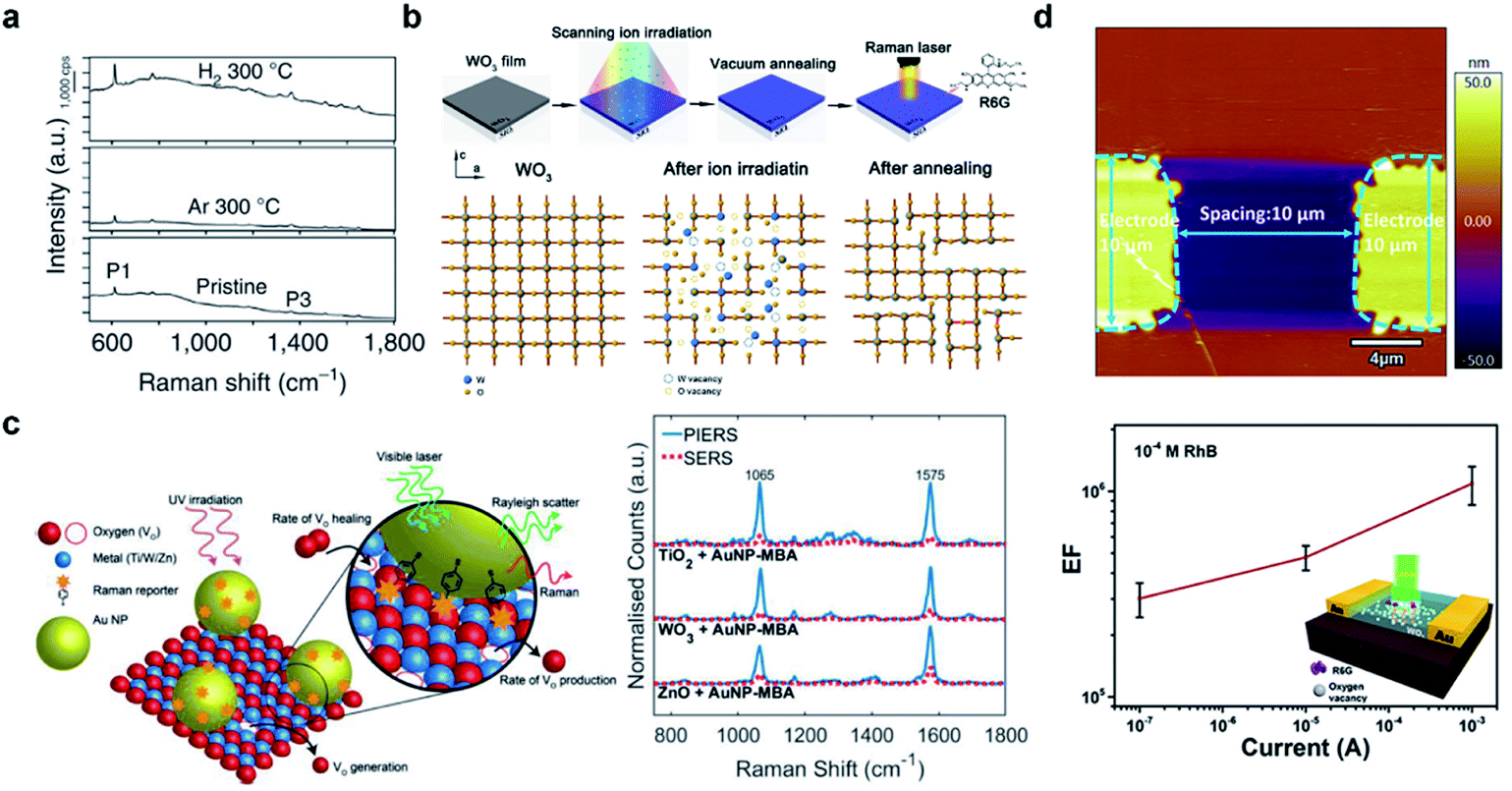 | ||
| Fig. 1 Vacancy-induced SERS-active semiconductor substrates. (a) SERS spectra of R6G on pristine and Ar/H2-treated W18O49. Reproduced with permission from ref. 26. Copyright 2015, Springer Nature. (b) Fabrication and SERS evaluation of ion-irradiated WO3 thin films. Reproduced with permission from ref. 31. Copyright 2017, American Chemical Society. (c) Schematic illustration of the PIERS technique and SERS performance of semiconductors before and after UV irradiation. Reproduced with permission from ref. 32. Copyright 2019, John Wiley and Sons. (d) AFM topographical image and SERS evaluation of the electrically tuned WO3 substrate. Reproduced with permission from ref. 36. Copyright 2019, American Chemical Society. | ||
In addition to OVs, other types of vacancies have also been studied. Copper vacancies in cuprous oxide systems have been shown to enhance surface adsorption and SERS of R6G, CV, 4ATP and Sudan Red III.38–40 S vacancies in MoS2 were studied by Zuo et al.41 Through femto-second pulse laser treatment, a significant number of micro/nanoscale defects and S vacancies were introduced, which were responsible for enhanced physical–chemical adsorption of molecules and consequent SERS activity, raising the EF towards R6G by 6-fold compared with that of pristine MoS2.
2.2 Dopants
Extrinsic doping is another widely applied means of introducing defects into the material lattice. Depending on parameters such as the radius and charge of the dopant atom, the dopant could enter the host lattice by substituting the atoms of the host, or by intercalating into spaces between the lattice. Through controlling the type and concentration of the dopant, the intrinsic crystalline and electronic structure, and surface properties of the host material can be manipulated.Cationic doping is very well established in SERS research. Small size cations such as H+, Li+, Na+ and Al3+ are usually easily intercalated into the crystal lattice due to their small size. Yang et al.42 reported the hydrogenation of black TiO2 nanowires (Fig. 2a), which boosted SERS activity and photocatalytic self-cleaning ability of the substrate due to doping-induced formation of surface defects. Cong et al. reported electrochemical intercalation of IA–IIIA group cations into amorphous WO3 thin films (Fig. 2b), which resulted in greatly enhanced detection of R6G.43 This facile approach gives easy access to large-scale, uniform, reproducible and renewable fabrication of SERS-chips. Transition metal dopants are also a popular choice to create defects, which is especially helpful for enhancing optical properties of broad band semiconductors, as they contain ample d-orbitals that act as charge acceptors in photoinduced CT processes. Zhao and co-workers have conducted a series of research studies on the doping of metal oxides TiO2 (ref. 44–46) and ZnO47 with transition metals, showing improved optical responses and SERS activity at the optimal doping concentration. Zheng et al.48 showed that the doping of Co induced strong optical absorption in the vis-NIR region in MoO3−x, resulting in synchronous SERS detection and photothermal conversion. More recently, research on rare earth metal doping has also presented interesting findings. Rare earth metals, which have highly variable valence states and electronic states, have been shown to endow the host semiconductor with useful luminescent, electromagnetic, conductive and electrochemical properties.49,50 Yang et al.51 reported Nd-doped ZnO, where the Nd dopant successfully enhanced the SERS detection for 4-MPY, and can be used to monitor the CT processes created due to Nd-related energy states. Due to their unique electronic structure, rare earth dopants have potential for enhancing CM-mediated SERS activity in semiconductors, which surpasses current reports.
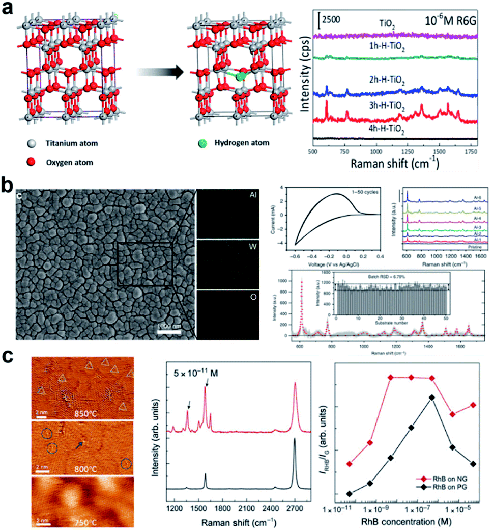 | ||
| Fig. 2 Doped semiconductor substrates and SERS activity. (a) Crystal structure of TiO2 and hydrogenated TiO2 and Raman spectra of R6G on TiO2 with different levels of hydrogenation. Reproduced with permission from ref. 42. Copyright 2018, American Chemical Society. (b) EDX analysis of Al-intercalated WO3 and its SERS performance characterization. Reproduced with permission with ref. 43. Copyright 2019, Springer Nature. (c) STM images of N-doped graphene under different synthesis conditions and SERS performance characterization. Reproduced with permission from ref. 61. Copyright 2016, AAAS. | ||
Anionic doping with non-metallic impurities has been extensively studied, particularly in two-dimensional materials.52–60 Nitrogen, a commonly used reductive dopant, can be easily introduced into the host structure by sample-treatment in a NH3 or N2 atmosphere. Feng et al.61 showed significantly boosted SERS sensitivity in N-doped graphene, with an impressive detection level of 5 × 10⁻¹¹ M for RhB (Fig. 2c). In another example, quantum-scale graphite doped with N62 exhibited enhancement towards 100 nM CV with the maximum EF reaching 3.2 × 10⁷. Oxygen doping has also been investigated. Huh et al.57 reported activated SERS in oxidized graphene, by treating graphene with UV/ozone irradiation, increasing the EF of pristine graphene from 103 to 104. Oxygen doping of TMD nanosheets was reported by Zheng et al.63 by careful annealing of samples in an air atmosphere. At the appropriate concentration, oxygen incorporation induced strong SERS activity towards R6G in MoS2, MoSe2, WS2, and WSe2. To summarize, both cationic and anionic dopants are good candidates for tuning the electronic and surface properties of the host material, towards boosting its SERS performance. As shown in this section, cationic dopants appear to be preferable compared with anionic dopants due to the relatively facile experimental requirements for cationic doping and wider selection of cationic dopants (most transition and main group elements have been reported). In future investigations, we speculate that improved material engineering techniques will greatly aid the construction of doped semiconductors with greater variety and complexity, which will expand the selection of available SERS-active semiconductors.
2.3 Lattice disorders
In the above sections we have dealt with point-defect type materials, which constitute the main body of defect-related reports in semiconductor-based SERS. However, more complex defect types have also been considered. Lattice disorders, which can cover a variety of defects such as line defects, planar defects or bulk defects, have also received increased attention.One notable form of lattice disorder is amorphous materials. In the case of amorphous structures, the entire lattice can be viewed as highly disordered due to the absence of long-range ordering, which effectively provides plentiful defective sites for surface interactions. Some prototype amorphous semiconductor substrates have been studied, including amorphous TiO2 (ref. 64) (Fig. 3a), ZnO,65 Rh3S6,66 HxMoO3 (ref. 67) and metal hydroxide (M(OH)x) nanostructures.68 The promoted SERS activities in amorphous structures are predominantly due to enhanced surface adsorption and promoted interfacial CT, resulting from abundant surface defect sites.
 | ||
| Fig. 3 Semiconductors with lattice disorders and their SERS performances. (a) The HRTEM micrographs of amorphous TiO2 nanosheets and Raman spectra of 4-MBA on crystalline and amorphous TiO2. Reproduced with permission from ref. 64. Copyright 2019, American Chemical Society. (b) HAADF-STEM image of the ultrathin WO3 nanosheet with surface defects, and Raman spectra of MB on the WO3 bulk material and ultrathin nanosheets. Reproduced with permission from ref. 69. Copyright 2021, John Wiley and Sons. (c) Self-assembly process for the formation of Cu2O cube-like superstructures by lattice fusion, and SERS enhancement comparison between different morphologies of Cu2O. Reproduced with permission from ref. 38. Copyright 2016, John Wiley and Sons. | ||
Lattice disorders can also be spontaneously created by morphological tuning. Song et al. proposed that ultrathin metal oxide nanosheets spontaneously lose lattice oxygen due to their low dimensional structure, forming point defects and distortions in the lattice cell in order to maintain structural stability within the crystal (Fig. 3b).69 As a result, the substrate–molecule interfacial CT can be promoted. The advantage of inducing defects in ultrathin nanosheets is that the crystalline form of the material can be retained, while ample localized surface defects serve as the main sites for highly efficient interfacial interactions. Consequently, the approach has been found to substantially promote the SERS behavior of WO3, MoO3 and MnO2. Lattice fusion in special morphologies can also promote localized defects. In Cu2O superstructures assembled from Cu2O mesoporous spheres (MPS), Lin et al.38 demonstrated the creation of a higher Cu vacancy content than that in Cu2O cubes or single MPS, attributed to the lattice fusion between adjacent spheres (Fig. 3c). The detection limit for R6G on the Cu2O superstructures consequently reached an ultralow level of 6 × 10⁻⁹ M. Similar morphology-driven lattice fusion leading to high SERS activity has also been observed in ZnO.70
Phase engineering is also useful for inducing defects in some semiconductors. Miao et al.71 showed that three phases of VO2 exhibited distinctly different levels of SERS activity, which was attributed to structure-originated differences in the tolerance for defects. The monoclinic phase VO2(B) which consists of a layered structure was found to exhibit the highest SERS activity due to a higher tendency to accommodate oxygen vacancies. Patil et al.72 developed a series of one-step hydrothermal procedures that produced MoO3 crystals of different crystal phases, which simultaneously demonstrated the inherent optical response and SERS activity of defective h-MoO3 and α-MoO3.
2.4 Metallic semiconductors
A special type of semiconductor must be mentioned here, namely metallic semiconductors which exhibit LSPR activity. Metallicity in semiconductors refers to their properties to transport electrons, which becomes prominent when the charge carrier density and density of states near the Fermi level increase.73 Metallicity is of interest in SERS as CT-based enhancement and plasmonic resonance-based enhancement are directly influenced by the metallicity of the semiconductor. Defect engineering, which causes changes to the charge carrier density and electronic structure is therefore a convenient approach to increase metallicity in semiconductors. For most semiconductors, only weak LSPR activity is promoted by their increased defect-induced metallicity, nevertheless the LSPR contribution can be coupled with simultaneously enhanced CT contributions to synchronously improve SERS performance. Moreover, in some semiconductors, sufficient LSPR activity within Raman-appropriate frequencies can be produced. Typical examples of metallic semiconductors that are SERS-active due to high LSPR activity are Mo-based compounds. Strikingly, Xi and co-workers have notably reported several metallic Mo-based semiconductors which have been successfully used to detect several small organic molecules with reasonably low LOD, showing general applicability of metallic semiconductors as SERS sensors. Compared with semiconducting MoO3, the more oxygen-deficient MoO2 nano-dumbbells exhibit a high density of free electron gas that forms nonpolar Mo–Mo metallic bonds (Fig. 4a).74 These characteristics promoted the surface plasmonic resonance at 532.8 nm laser excitation, contributing to high SERS activity. In addition to R6G, several polychlorinated phenol molecules were also detected at sub-micromolar concentrations. Moreover, the plasmonic activity of MoO2 nanostructures can be further enhanced by introducing oxygen vacancies, as was shown by Cao et al.75 who induced surface oxygen vacancy sites by reductive treatment with lithium (Fig. 4b). Similar to MoO2, metallic Mo2N and MoN nanostructures have also showed plasmonic activity.76–78 In addition to molybdenum oxides and nitrides, Ti3O5, TiN and VO2 with high EM activity have also been reported.79–81 As LSPR is a non-selective enhancing effect, the conditions for LSPR-mediated SERS are not as stringent as CT-mediated effects, making LSPR semiconductors more adaptive towards different probe molecules.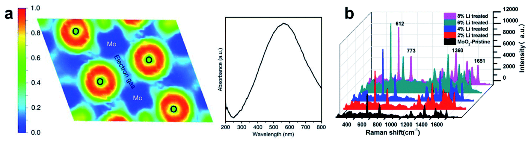 | ||
| Fig. 4 Semiconductors with LSPR activity. (a) LSPR activity of MoO2 nano-dumbbells. Reproduced with permission from ref. 74. Copyright 2017, Springer Nature. (b) SERS image of R6G on lithium-treated oxygen-vacancy-rich MoO2−x. Reproduced with permission from ref. 75. Copyright 2019, American Chemical Society. | ||
3. Influences of defect engineering on semiconductors
The introduction of defects causes changes in several important parameters of semiconductor materials, which are directly related to their SERS activity. In this section, we introduce the three key parameters that can be regulated by defect engineering, namely the band structure, surface properties and DOS, as well as their respective relationships to SERS activity by referring to the fundamental theories of SERS.3.1 Regulation of the band structure
The possibility for CT resonance to occur is the matching of the band structure in such a way that the energy discrepancy of the CT process is in close proximity to the laser energy. As many semiconductors generally do not exhibit strong surface plasmonic behavior, their SERS activity relies heavily upon CT resonances, which include intrinsic excitonic CT processes (μex) and substrate–molecule CT processes (μPICT). Additionally, as vast numbers of semiconductors are wide-gap, requiring high energy (UV light) excitation, μex is difficult to apply to SERS applications which generally favor low energy excitation. For this reason, band structure tuning is particularly important for semiconductor-based SERS.Bandgap shrinkage, sometimes observed in doped semiconductors due to the band gap renormalization effect, could reduce the excitation energy threshold for μex.63,82–84 For instance, in oxygen-incorporated MoS2 nanosheets (Fig. 5a),63 significant shifts of the CB and VB edges resulted in a narrowed bandgap that closely matched the energy of the incident laser (2.33 eV). Moreover, newly created direct excitonic pathways in the bandgap further increased the population of effective μex resonance. Such a phenomenon has also been observed in other low dimensional TMDs.85,86 In extension to TMDs, μex resonance has also been achieved in trichalcogenide alloy MnPSxSe1−x by controlling the concentration of Se towards similar effects of band gap tuning.87
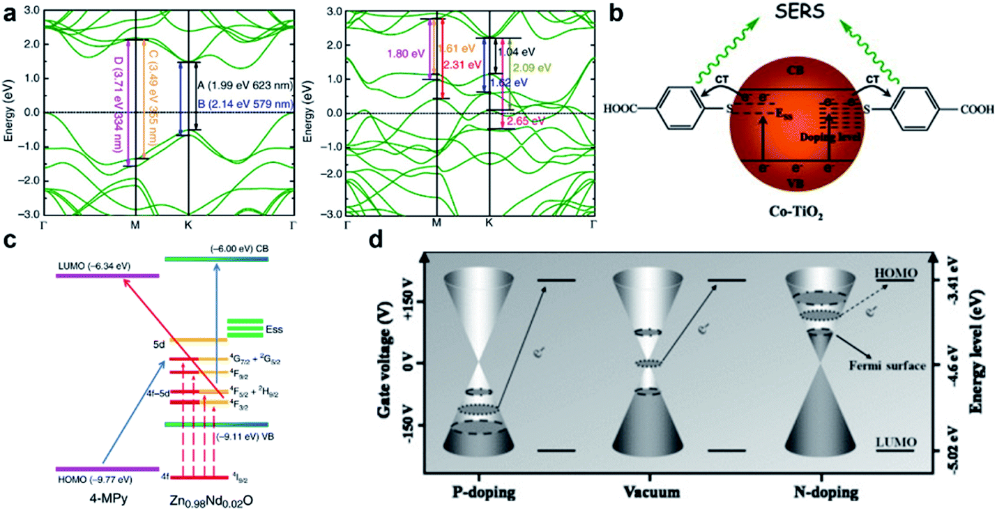 | ||
| Fig. 5 Regulation of the band structure in semiconductors by defects. (a) Band structures of MoS2 before and after oxygen incorporation. Reproduced with permission from ref. 63. Copyright 2017, Springer Nature. (b) CT process from VB to ESS and dopant-related states in Co-doped TiO2, and from defective states to adsorbed 4-MBA. Reproduced with permission from ref. 90. Copyright 2014, Elsevier. (c) CT processes between 4-MPY and Nd-doped ZnO. Reproduced with permission from ref. 51. Copyright 2020, Springer Nature. (d) Electrical modulation of CT enhancement in GERS by the manipulation of the Fermi level under different types of doping conditions. Reproduced with permission from ref. 91. Copyright 2011, John Wiley and Sons. | ||
In addition to the band gap, new energy states could be created due to various types of defects. Defect-induced disorders often cause the formation of surface state levels (ESS),88–90 which is useful for inducing electron transition from the VB with lower excitation energy. Doping will introduce new energy states via the impurity atom, in addition to ESS levels, as is shown in the example of CT from ESS and dopant-related states in Co-doped TiO2 to 4-MBA90 presented in Fig. 5b. The advantage of this strategy was also most effectively demonstrated by the doping of Nd in ZnO (Fig. 5c), in which several new absorption bands corresponding to the 4f, and 5d orbitals of Nd appeared in the visible light region.51 As a result, the number of μPICT and μex pathways is optimally increased, as was observed in the case of enhanced detection of 4-MPY.
The Fermi level (EF) is also tunable by defect engineering. In graphene particularly, the Fermi level is an important tunable parameter that is greatly affected by the electronegativity of the dopant. Xu et al.91 conducted a careful investigation of CT modulation in the SERS signal of CuPc on N- and O-doped graphene, illustrating that the CT between the Fermi level of graphene and LUMO of CuPc is greatly influenced by the dopant-dependent position deviation of EF from the Dirac point (Fig. 5d). They also investigated a series of metal-phthalocyanine (M-Pc) molecules,92 finding that in all cases the n-doped graphene (EF up-shifted) performed worse than p-doped graphene (EF down-shifted), which was attributed to the optimal matching of EF-LUMO energy discrepancy with the laser energy on p-doped graphene.
3.2 Regulation of active surface sites
In addition to the possibility of new CT pathways created by favorable energy matching, the actual establishment of effective CT channels depends crucially on the substrate–molecule surface interaction. Defect sites in semiconductors are often crucial to surface interactions. In the first place, for metal-based compounds undersaturated metal cations can serve as binding sites for the probe molecule. For instance, CO adsorption is found to be crucially facilitated by the bonding between CO and coordinately undersaturated Cu+ sites in Cu2O.93 Different metal sites could have different affinities towards a given probe molecule. Hurst et al.94 investigated the SERS effect of dopamine (characterized by the enediol ligand) functionalized on the surface of Fe2O3, TiO2, CeO2 and ZrO2 nanoparticles, which showed varied number, shift and intensity of Raman scattering signals, evidencing the formation of different CT complexes and their different optical responses which are dependent on the chemical composition. The disruption of the periodic array by defects induces the formation of dangling bonds at the surface, which are unbonded orbitals localized at undercoordinated surface metal centers. These dangling bonds can be capitalized to create sites of strong substrate–molecule interactions and effective CT, as have been observed in highly defective structures. Amorphous materials have an advantage in this regard due to their lack of long-range ordering. The amorphous surfaces in ZnO nanocages,65 for example, are richly populated by dangling bonds which causes thiols to form stronger Zn–S bonds that act as CT channels, as well as allowing for more effective electron transfer due to weaker electron constraint (Fig. 6a). Titanium oxide nanostructures have also been a prototypical subject of study for surface tuning due to their well-known affinity towards multiple functional groups. It has been pointed out that dangling oxygen species (Ti–O) formed in small TiO2 nanoparticles and their hydrogenated form can be highly active towards phenolic molecules such as dopamine, catechol and hydroquinone, both as binding sites and to facilitate CT.95–97 Based on this, Lewis and Brønsted surface sites can be produced as a result of defect-tuning. Gong et al.98 showed that with the substitution of SO42− ions for O2− in the TiO2 lattice, Lewis acid sites are produced due to the bidentate coordination of SO42− ligands to central Ti sites, while Brønsted acid sites are produced by the hydrogenated Ti–OH+ surface sites, resulting in the enhancement of TiO2–molecule CT interactions and subsequent SERS activity towards the molecule 4-MBA (Fig. 6b).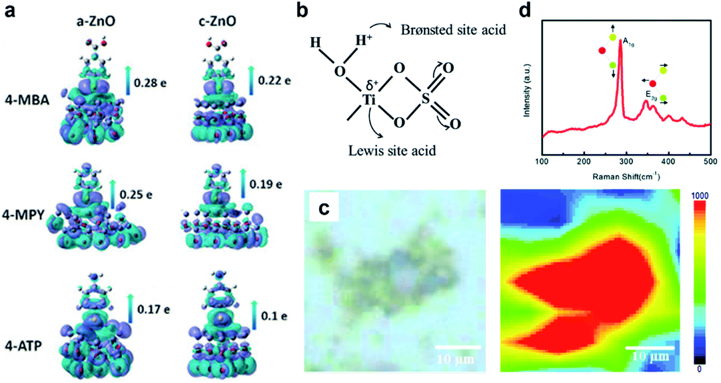 | ||
| Fig. 6 Surface activities between semiconductors and probe molecules. (a) Total electron density distributions of probe molecules chemically adsorbed onto the surface of amorphous ZnO (a-ZnO) and crystalline ZnO (c-ZnO). Reproduced with permission from ref. 65. Copyright 2017, John Wiley and Sons. (b) Brønsted and Lewis acid sites present on the H2SO4-treated TiO2 surface. Reproduced with permission from ref. 98. Copyright 2015, the Royal Society of Chemistry. (c) Optical and SERS mapping image of R6G (1362 cm−1) on Li-exfoliated MoS2. Adapted with permission from ref. 101. Copyright 2017, the Royal Society of Chemistry. (d) Raman spectrum of monolayer Janus MoSSe exhibiting a strong out-of-plane vibration. Reproduced with permission from ref. 102. Copyright 2020, the Royal Society of Chemistry. | ||
Van der Waals-type (vdW) nanosheets should also be discussed, as their SERS activity mainly originates from dipole–dipole interactions. Ling et al.99 first reported that in polar vdW structures such as h-BN (containing polar B–N bonds) and MoS2 (containing polar Mo–S bonds), increased probability of electron transition can be induced by local symmetry-perturbation upon interface dipole–dipole interactions with the probe molecule, which in turn contributes to SERS activity. Based on the nature of dipole–dipole interactions, the process can be enhanced by strengthening the polarity of chemical bonds in the vdW structures. With plasma treated MoS2, Sun et al.100 demonstrated the correlation between the amount of structural disorder and the formation of local dipoles which enhanced the overall SERS. Anbazhagan et al.101 proposed that in lithium-exfoliated MoS2, surface S and Mo vacancies are created that can promote dipole–dipole interactions with R6G, resulting in better substrate–molecule CT (Fig. 6c). The direction of substrate dipoles also affects dipole–dipole interactions greatly. Jia et al.102 engineered a 2D Janus MoSSe structure which generates out-of-plane dipoles due to the asymmetry of S–Mo–Se, enabling strong substrate–molecule interactions (Fig. 6d). Impressively, Janus MoSSe was successfully applied to the SERS detection of glucose, reaching a detection concentration of 1 mM and achieving an EF of 4 × 10⁵. These results indicate that although the dipole–dipole contribution is considered to account for a relatively small EF, the alteration of the bond polarity and structural symmetry in vdW nanosheets via defect engineering may very well lead to great improvement in their SERS performances.
3.3 Regulation of DOS
Upon establishing the probability and channel for CT occurrence, the efficiency of the CT process is the third key factor that influences SERS activity. Fermi's golden rule (eqn (1))103,104 states that the electron transition probability rate (ωab) depends on the density of the final states (gb), and the strength of the matrix element |〈b|M|a〉|2, namely the initial and final state (|a〉, |b〉) of the charge transition.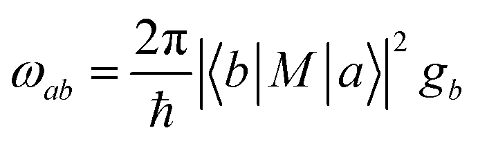 | (1) |
As such it may be said that the DOS of the states relative to a given CT process is positively correlated with the efficiency of that CT process. Cong et al. demonstrated this defect-driven effect with metal-cation-doped WO3 thin films.43 Taking Al3+ ions as an example, it was found that the DOS near EF of WO3 is linearly correlated with the concentration of Al3+ and also positively affects the SERS signal of R6G (Fig. 7a). In addition to the increase in DOS, simultaneous accumulation of electrons in the W 5d orbitals also occurred which also served to increase the population of μPICT. Following this, the same phenomenon has been observed in other SERS systems. Song et al. found that the surface oxygen defects created in ultrathin WO3 nanosheets also increased the DOS near EF, which enhanced the SERS effect for MB (Fig. 7b).69 The DOS increase related to defects has also been found in TMDs such as defective MoS2 and WSe2 (Fig. 7c).41,63,105,106
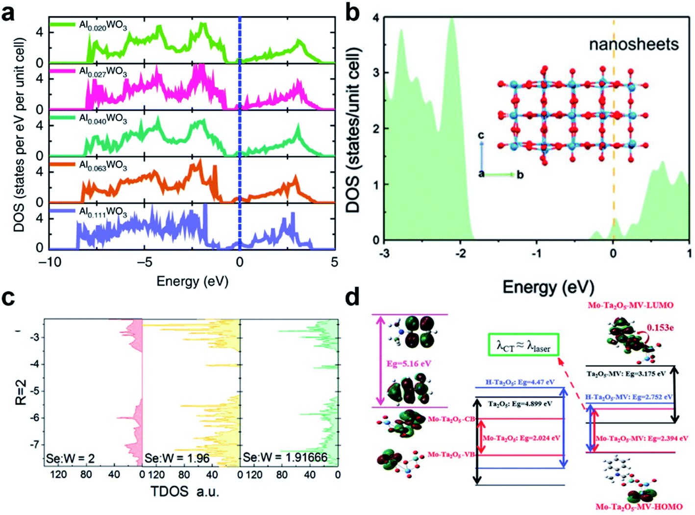 | ||
Fig. 7 Manipulation of DOS in semiconductors by defect engineering. (a) DOS of different concentration Al-doped WO3. Reproduced with permission from ref. 43. Copyright 2019, Springer Nature. (b) DOS of simulated ultrathin WO3 nanosheets. Reproduced with permission from ref. 69. Copyright 2021, John Wiley and Sons. (c) TDOS of WSe2 with different W![[thin space (1/6-em)]](https://www.rsc.org/images/entities/char_2009.gif) :Se atomic ratios. Reproduced with permission from ref. 105. Copyright 2018, John Wiley and Sons. (d) Illustrations of CT resonance processes in different MV–Ta2O5 complexes. Reproduced with permission from ref. 25. Copyright 2019, John Wiley and Sons. :Se atomic ratios. Reproduced with permission from ref. 105. Copyright 2018, John Wiley and Sons. (d) Illustrations of CT resonance processes in different MV–Ta2O5 complexes. Reproduced with permission from ref. 25. Copyright 2019, John Wiley and Sons. | ||
Lastly, it should be pointed out that an increased charge carrier density also leads to the surface plasmonic effect,107 which has been observed in most defective materials mentioned in this perspective and can be simply characterized by the Urbach tail in the absorption spectra. Although the peak frequency of LSPR for most defective semiconductors falls beyond an applicable range as stated in 2.4, limiting the impact of the surface plasmonic effect to their overall SERS activity, their contributions should still be taken into account. Moreover, EM contributions such as surface plasmon and Mie resonance effects can be coupled with CM-based contributors towards the highly activated multi-coupled SERS effect. Such an amalgamation has been successfully implicated in the system of Mo–Ta2O5–MV, proposed by Yang et al., in which the coupling of μPICT, molecular resonance (μmol) and EM effects resulted in an overall EF of 2.2 × 10⁷ and LOD of 9 × 10⁻⁹ M towards the probe MV (Fig. 7d).25
4. Applications of SERS-active defective semiconductors
The advantages of higher interfacial CT and molecule-selective interactions afforded by defective semiconductors make them uniquely suitable for specialized SERS sensing applications. The applications of semiconductor-based SERS platforms can be divided into two major categories. The first includes sensors for ex situ detection of chemical species, in other words sensors that are used in the conventional laboratory setting. Such sensors are usually of interest in analysis of food, environment, industrial products or biological samples. The second includes sensors for in situ analysis, usually for characterization of chemical reactions or CT processes in a device. In such cases the semiconductor may play multiple functions, such as acting as a catalyst and SERS sensor.4.1 Ex situ sensing
Ex situ trace sensing platforms often involve samples with a complex chemical composition, and require quantitative detection of the target with minimal interference signal. In these scenarios the band structure and surface properties of semiconductors controlled by defect engineering can be especially useful. In environmental analysis, the detection of small ionic species such as Cr(VI) and PO43− in water samples has been achieved with colloidal TiO2 nanoparticles with rich surface hydroxyl groups.108,109 Hydroxyl-group-rich TiO2 colloids are also especially selective towards phenolic molecules, and have been proposed as SERS sensors for quantitative analysis of phenolic polymer inhibitors in olefins.97 In food analysis, methods for the detection of prohibited substances are in high demand. Recently, a SERS-chip for detection of Sudan Red III in Chinese medicinal herbs was developed using defective Cu2O nanostructures (Fig. 8a).40 Biochemical sensing has also seen advances in recent years, with the range of detected bioactive species expanding rapidly, from biorelevant small molecules such as β-sitosterol and bilirubin to larger structures such as DNA.110–112 Cancerous cells and biomarkers related to cancer are now detectable using a variety of semiconductor materials. VEGF, a biomarker for brain tumor, was detected using aptamer-functionalized WO3.113 Defective Ag2O nanoparticles functionalized with folic acid have been constructed to selectively bind to cancer cells in blood, showing clear distinction in SERS spectra between liver cancer patients and healthy individuals (Fig. 8b).114In vitro mapping of cancer cells and their genomic DNA has been achieved with quantum sized semiconductors.115–117 Quantum sized oxygen-deficient TiOx particles were developed for detection of tumor biomarker EGFR (Fig. 8c),117 exhibiting good cell adherence and low cytotoxicity. SERS analysis showed clear EGFR signals and a higher lipid content in breast cancer cells compared to non-cancerous fibroblast cells. The report also showed distinct SERS features for cervical cancer cell line HeLa. In addition to biosensing, therapeutic functions have also been achieved. Particularly, NIR-responsive semiconductors are extensively used in photothermal treatment (PTT) of cancerous cells, including hydrous RuO2, WS2, copper chalcogenides and Mo-based materials.72,118–122 Photo-tuned MoO2 quantum dots with varied optical responses in the NIR region are a good example of dual-functional SERS substrates,122 with SERS activity towards bioactive molecules phenylalanine and amphotericin, and also showing good PTT performance towards cancer cell line HEP G2.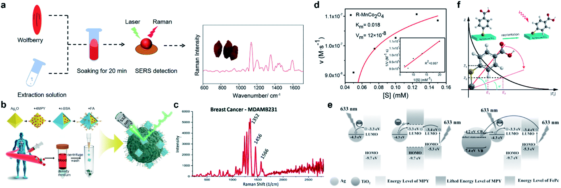 | ||
| Fig. 8 Applications of defective semiconductor-based SERS. (a) Detection of Sudan Red III in Chinese herbal medicines. Reproduced with permission from ref. 40. Copyright 2021, John Wiley and Sons. (b) Detection of tumor cells on functionalized Ag2O substrates. Reproduced with permission from ref. 114. Copyright 2021, Springer Nature. (c) SERS detection of breast cancer cells. Reproduced with permission from ref. 117. Copyright 2019, the Royal Society of Chemistry. (d) SERS-kinetic assay of TMB oxidation. Reproduced with permission from ref. 127. Copyright 2020, American Chemical Society. (e) Photoinduced CT process in TiO2–Ag–MPY–FePc systems. Reproduced with permission from ref. 128. Copyright 2019, John Wiley and Sons. (f) Physical model of 4-MBA molecule movement on the surface of the Ag/Ag-doped TiO2 substrate under laser irradiation. Reproduced with permission from ref. 35. Copyright 2020, Springer Nature. | ||
4.2 In situ sensing
The SERS technique has been especially favored in monitoring chemical reactions that take place in aqueous environments, as the interference of water signals can be minimized by Raman spectroscopy. The detection of intermediate or product species in a reaction does not usually require quantification, but requires high sensitivity and good surface adherence towards the target, which can be met by defective semiconductors that have tunable surfaces and high CT-induced SERS activity. Proof-of-concept studies of SERS in monitoring biochemical reactions have been proposed. Alessandri and Depero123 demonstrated the use of all-oxide substrates in the monitoring of the glutathione (GSH) redox reaction with a core–shell structure of SiO2 coated with amorphous TiO2. Han et al.124 demonstrated the SERS monitoring of the redox behavior of cytochrome b5 (Cyt b5), a hemoprotein, using TiO2 as the substrate. In addition to probing biochemical reactions, SERS-active semiconductors tend to also exhibit catalytic properties, which naturally intrigues research into establishing a SERS-based methodology to characterize catalytic processes at the molecular level. Zhang et al.125 studied the photo-oxidation of silane to silanol on the CuO surface. The production of *OH species is identified in situ, which is attributed to the oxygen vacancies on the CuO surface which act as absorption and activation sites for H2O2. In another example, Wen et al. have studied the nanoenzyme properties of reduced MnCo2O4 with the aid of Au NPs to boost its SERS activity.126 They also reported a SERS-kinetic model which monitored the oxidation of tetramethylbenzidine (TMB), based on reduced MnCo2O4 nanotubes, which had the double function of the SERS substrate and oxidase (Fig. 8d).127 The highlight of the work is the access to in situ monitoring of the oxidization process based on quantitative SERS analysis of the oxidized TMB product (oxTMB) on the surface of oxygen-vacancy-rich MnCo2O4. It should be noted that while the CT-induced SERS performance of reduced MnCo2O4 nanotubes improved compared to that of pristine MnCo2O4, their oxidase-like catalytic activity slightly declined, which shows that the influence of defect engineering on SERS and catalytic activity differs.In extension to the monitoring of isolated reactions, the demand for SERS characterization of more complex model systems and devices has also been on the rise.128–132 It is well established that the CT effect can selectively influence the enhancement of specific molecules or specific vibrational modes, therefore the relative signal intensity of selected bands in the SERS spectrum can be used to reflect the degree of CT (ρCT) and the site of the reaction. This method has been extensively studied in solar-cell-like model systems. Wang et al.128 reported the use of a combined Ag–TiO2–FePc–MPY structure to demonstrate the manipulation of the CT direction based on band energy matching between components, which was reflected in the change of ρCT for selected SERS bands (Fig. 8e). This work is useful for guiding the design of solar-cell model structures and predicting the CT direction. In another instance, the CT-based change in SERS spectra has also been used to monitor the movement of surface adsorbed molecules35(Fig. 8f). By monitoring the Raman frequency shift of 4-MBA adsorbed on a Ag/Ag-doped TiO2 substrate under NIR irradiation, the reorientation of the molecule due to accumulated CT-induced electrostatic attraction can be observed. In organic photovoltaics, Luke et al.132 reported the use of in situ Raman spectroscopy in monitoring the degradation process of organic photovoltaic devices, offering a practical methodology for understanding chemical reaction processes in devices.
5. Conclusion and outlook
In this perspective we have introduced defect engineering towards enhancing SERS activity in semiconductors, and discussed mechanisms behind the SERS activity of defective semiconductors. While the rapid development of novel semiconductor platforms can be credited in large part to defect engineering techniques, there is still much to be explored in the field. To begin with, defect engineering in SERS has mainly focused on point defects, while influences of more complex defects on the physicochemical parameters and SERS activities of semiconductors have not yet been fully investigated. For instance, research into SERS-activity as influenced by line defects, planar defects or volumetric defects has been limited. It could be argued that while introduction of vacancies and extrinsic dopants is facile and generally applicable to defect engineering strategies, the study of higher dimensional defective systems (lattice disorders and metallic semiconductors) may reveal novel SERS-promoting mechanisms and deepen our understanding of the fundamental relationship between defects and SERS activity. Second, the range of defective semiconductors that are under research has been largely limited to prototypical materials such as TiO2, graphene and MoS2. With the expanding range of novel semiconductors, the selection of materials for SERS applications has also grown to include materials such as MOFs, organic semiconductors and MXenes. New defect engineering techniques suited to each semiconductor category and new insights into the mechanisms behind SERS phenomenon will likely rise from these novel classes of materials. Third, refining the stability and reproducibility of defects in semiconductor-based SERS substrates will be an important issue. As SERS substrates are often expected to be deployed under complex working conditions, the production of SERS-active defective semiconductor materials which can maintain stability and signal reproducibility in complex systems will be of great significance.The applications of semiconductor-based SERS were also discussed. Environmental analysis, food safety, biosensing and reaction monitoring in devices are all important branches of research with very different analysis requirements that may benefit from the development of novel SERS platforms. Current research interests suggest that SERS-sensing is increasingly moving towards in situ or point-of-care testing scenarios. However, present design of semiconductor-based platforms still requires variety to meet the specific demands of specialized detection. In this regard, the high tunability of semiconductor surfaces and chemical properties can be a great advantage for tailoring the SERS platform to suit the testing environment. Future research might focus on the selective adherence of substrates towards target species based on the tuning of surface properties of semiconductors, and regulating parameters of the optical response towards achieving highly sensitive SERS substrates. Moreover, deeper insight into defect engineering may help improve understanding of the design of multi-functional semiconductors which facilitate SERS along with other properties such as catalytic or photothermal activities.
The SERS phenomenon is complex in principle and still under investigation. The recent development of defect engineering in semiconductor-based SERS has greatly pushed the boundaries of the field, with the realization of increasingly high quality and sophisticated sensing platforms. We hope that this perspective provides fellow researchers with basic knowledge for designing semiconductor-based SERS substrates and that they might be inspired to perform deeper examinations of defect engineering and its uses in SERS research.
Author contributions
The manuscript was written through contribution from all the authors. G. S., S. C. and Z. G. Z. conceived the main outline of the manuscript. G. S. wrote the first draft of the manuscript. S. C. and Z. G. Z. discussed and helped revise the manuscript.Conflicts of interest
There are no conflicts to declare.Acknowledgements
The authors acknowledge support from the following sources: National Key R&D Program of China 2020YFB1505703; The National Natural Science Foundation of China 52172299, 22175198, 51772319, 51772320, and 51972331; Key Laboratory of Nanodevices of Jiangsu Province Y4JAQ21004; Pilot Project of Fundamental Research of Suzhou City; External Cooperation Program of the Chinese Academy of Sciences 121E32KYSB20190008; Six Talent Peaks Project of Jiangsu Province XCL-170; Youth Innovation Promotion Association, CAS 2018356; Outstanding Youth Fund of Jiangxi Province 20192BCBL23027.Notes and references
- H. Lim, D. Kim, Y. Kim, T. Nagaura, J. You, J. Kim, H.-J. Kim, J. Na, J. Henzie and Y. Yamauchi, J. Mater. Chem. A, 2020, 8, 21016–21025 RSC.
- A. Karmakar, K. Karthick, S. S. Sankar, S. Kumaravel and S. Kundu, Appl. Surf. Sci., 2020, 527, 146777 CrossRef CAS.
- T. Zhang, Y. Sun, L. Hang, H. Li, G. Liu, X. Zhang, X. Lyu, W. Cai and Y. Li, ACS Appl. Mater. Interfaces, 2018, 10, 9792–9801 CrossRef CAS PubMed.
- D. Kim, J. Kim, J. Henzie, Y. Ko, H. Lim, G. Kwon, J. Na, H.-J. Kim, Y. Yamauchi and J. You, Chem. Eng. J., 2021, 419, 129445 CrossRef CAS.
- Y. Zhai, H. Yang, S. Zhang, J. Li, K. Shi and F. Jin, J. Mater. Chem. C, 2021, 9, 6823–6833 RSC.
- H. Lim, D. Kim, G. Kwon, H.-J. Kim, J. You, J. Kim, M. Eguchi, A. K. Nanjundan, J. Na and Y. Yamauchi, J. Phys. Chem. C, 2020, 124, 23730–23737 CrossRef CAS.
- M. Chen, D. Liu, X. Du, K. H. Lo, S. Wang, B. Zhou and H. Pan, Trends Anal. Chem., 2020, 130, 115983 CrossRef CAS.
- H. Yamada, Y. Yamamoto and N. Tani, Chem. Phys. Lett., 1982, 86, 397–400 CrossRef CAS.
- J. Pan, M. Li, Y. Y. Luo, H. Wu, L. Zhong, Q. Wang and G. H. Li, Appl. Surf. Sci., 2015, 333, 34–38 CrossRef CAS.
- Y. Peng, C. Lin, M. Tang, L. Yang, Y. Yang, J. Liu, Z. Huang and Z. Li, Appl. Surf. Sci., 2020, 509, 145376 CrossRef CAS.
- L. Yang, Y. Wei, Y. Song, Y. Peng, Y. Yang and Z. Huang, Mater. Des., 2020, 193, 108808 CrossRef CAS.
- Y. Shan, Z. Zheng, J. Liu, Y. Yang, Z. Li, Z. Huang and D. Jiang, Npj Comput. Mater., 2017, 3, 11 CrossRef.
- F. Pan, G. B. Zhou, L. L. Huang, W. Li, M. S. Lin and C. Liu, Chin. J. Chem. Eng., 2020, 28, 889–895 CrossRef CAS.
- H. G. Zhang, H. W. Xin, T. J. He and F. C. Liu, Spectrochim. Acta Mol. Biomol. Spectrosc., 1991, 47, 927–932 CrossRef.
- D. W. Li, J. Wang, H. W. Xin, S. Xu and F. C. Liu, Spectrochim. Acta Mol. Biomol. Spectrosc., 1987, 43, 379–382 CrossRef.
- M. Dandu, K. Watanabe, T. Taniguchi, A. K. Sood and K. Majumdar, ACS Photonics, 2020, 7, 519–527 CrossRef CAS.
- Y. Yin, P. Miao, Y. M. Zhang, J. C. Han, X. H. Zhang, Y. Gong, L. Gu, C. Y. Xu, T. Yao, P. Xu, Y. Wang, B. Song and S. Jin, Adv. Funct. Mater., 2017, 27, 1606694 CrossRef.
- X. Ling, L. M. Xie, Y. Fang, H. Xu, H. L. Zhang, J. Kong, M. S. Dresselhaus, J. Zhang and Z. F. Liu, Nano Lett., 2010, 10, 553–561 CrossRef CAS PubMed.
- Z. Yu, W. L. Yu and C. L. Guo, Chin. Opt., 2019, 12, 952–963 CrossRef.
- Z. Yu, W. L. Yu, J. Xing, R. A. Ganeev, W. Xin, J. L. Cheng and C. L. Guo, ACS Photonics, 2018, 5, 1619–1627 CrossRef CAS.
- G. Demirel, R. L. M. Gieseking, R. Ozdemir, S. Kahmann, M. A. Loi, G. C. Schatz, A. Facchetti and H. Usta, Nat. Commun., 2019, 10, 5502 CrossRef CAS PubMed.
- M. Yilmaz, E. Babur, M. Ozdemir, R. L. Gieseking, Y. Dede, U. Tamer, G. C. Schatz, A. Facchetti, H. Usta and G. Demirel, Nat. Mater., 2017, 16, 918–924 CrossRef CAS PubMed.
- H. Sun, S. Cong, Z. Zheng, Z. Wang, Z. Chen and Z. Zhao, J. Am. Chem. Soc., 2019, 141, 870–878 CrossRef CAS PubMed.
- X. Hou, X. Tang, Y. Wei, S. Wang, Q. Hao, J.-M. Hou and T. Qiu, Cell Rep. Phys. Sci., 2021, 2, 100488 CrossRef.
- L. Yang, Y. Peng, Y. Yang, J. Liu, H. Huang, B. Yu, J. Zhao, Y. Lu, Z. Huang, Z. Li and J. R. Lombardi, Adv. Sci., 2019, 6, 1900310 CrossRef PubMed.
- S. Cong, Y. Yuan, Z. Chen, J. Hou, M. Yang, Y. Su, Y. Zhang, L. Li, Q. Li, F. Geng and Z. Zhao, Nat. Commun., 2015, 6, 7800 CrossRef CAS PubMed.
- Y. M. Yang, X. N. Gao, S. J. Yang, Y. H. Shen and A. J. Xie, J. Mater. Sci., 2021, 56, 9702–9711 CrossRef CAS.
- S. Lee, J. W. Peng and C. S. Liu, Appl. Surf. Sci., 2013, 285, 748–754 CrossRef CAS.
- Y.-b. Li, Y.-p. Liu, J. Wang, Y.-l. Guo and K. Chu, Inorg. Chem. Front., 2020, 7, 455–463 RSC.
- Y. Liu, X. Kong, X. Guo, Q. Li, J. Ke, R. Wang, Q. Li, Z. Geng and J. Zeng, ACS Catal., 2020, 10, 1077–1085 CrossRef CAS.
- X. Zheng, F. Ren, S. Zhang, X. Zhang, H. Wu, X. Zhang, Z. Xing, W. Qin, Y. Liu and C. Jiang, ACS Appl. Mater. Interfaces, 2017, 9, 14534–14544 CrossRef CAS PubMed.
- D. Glass, E. Cortes, S. Ben-Jaber, T. Brick, W. J. Peveler, C. S. Blackman, C. R. Howle, R. Quesada-Cabrera, I. P. Parkin and S. A. Maier, Adv. Sci., 2019, 6, 1901841 CrossRef CAS PubMed.
- S. Ben-Jaber, W. J. Peveler, R. Quesada-Cabrera, E. Cortes, C. Sotelo-Vazquez, N. Abdul-Karim, S. A. Maier and I. P. Parkin, Nat. Commun., 2016, 7, 12189 CrossRef CAS PubMed.
- O. E. Dagdeviren, D. Glass, R. Sapienza, E. Cortes, S. A. Maier, I. P. Parkin, P. Grutter and R. Quesada-Cabrera, Nano Lett., 2021, 21, 8348–8354 CrossRef CAS PubMed.
- L. Zhou, J. Zhou, W. Lai, X. Yang, J. Meng, L. Su, C. Gu, T. Jiang, E. Y. B. Pun, L. Shao, L. Petti, X. W. Sun, Z. Jia, Q. Li, J. Han and P. Mormile, Nat. Commun., 2020, 11, 1785 CrossRef CAS PubMed.
- C. Zhou, L. Sun, F. Zhang, C. Gu, S. Zeng, T. Jiang, X. Shen, D. S. Ang and J. Zhou, ACS Appl. Mater. Interfaces, 2019, 11, 34091–34099 CrossRef CAS PubMed.
- L. B. Yang, D. Yin, Y. Shen, M. Yang, X. L. Li, X. X. Han, X. Jiang and B. Zhao, Phys. Chem. Chem. Phys., 2017, 19, 22302–22308 RSC.
- J. Lin, Y. Shang, X. X. Li, J. Yu, X. T. Wang and L. Guo, Adv. Mater., 2017, 29, 1604797 CrossRef PubMed.
- S. Y. Fu, H. H. Chang, Y. K. Hsu and Y. G. Lin, Conference on Nanophotonic Materials XI, San Diego, CA, 2014 Search PubMed.
- Y. Jiang, S. Cong, G. Song, H. Sun, W. Zhang, W. Yao and Z. Zhao, J. Raman Spectrosc., 2021, 52, 1265–1274 CrossRef CAS.
- P. Zuo, L. Jiang, X. Li, P. Ran, B. Li, A. Song, M. Tian, T. Ma, B. Guo, L. Qu and Y. Lu, Nanoscale, 2019, 11, 485–494 RSC.
- L. L. Yang, Y. S. Peng, Y. Yang, J. J. Liu, Z. Y. Li, Y. F. Ma, Z. Zhang, Y. Q. Wei, S. Li, Z. R. Huang and N. V. Long, ACS Appl. Nano Mater., 2018, 1, 4516–4527 CrossRef CAS.
- S. Cong, Z. Wang, W. Gong, Z. Chen, W. Lu, J. R. Lombardi and Z. Zhao, Nat. Commun., 2019, 10, 678 CrossRef CAS PubMed.
- L. Yang, Y. Zhang, W. Ruan, B. Zhao, W. Xu and J. R. Lombardi, J. Raman Spectrosc., 2010, 41, 721–726 Search PubMed.
- L. B. Yang, X. Jiang and M. Yang, Appl. Phys. Lett., 2011, 99, 3 Search PubMed.
- X. X. Xue, W. Ji, Z. Mao, Z. S. Li, W. D. Ruan, B. Zhao and J. R. Lombardi, Spectrochim. Acta Mol. Biomol. Spectrosc., 2012, 95, 213–217 CrossRef CAS PubMed.
- X. Xue, W. Ruan, L. Yang, W. Ji, Y. Xie, L. Chen, W. Song, B. Zhao and J. R. Lombardi, J. Raman Spectrosc., 2012, 43, 61–64 CrossRef CAS.
- X. Zheng, X. Wang, Q. Tian, X. Cui, Y. Zhou, T. Ge, W. Liu, C. Wei and Q. Xu, Chem. Commun., 2020, 56, 7649–7652 RSC.
- Z. C. Zeng, Y. S. Xu, Z. S. Zhang, Z. S. Gao, M. Luo, Z. Y. Yin, C. Zhang, J. Xu, B. L. Huang, F. Luo, Y. P. Du and C. H. Yan, Chem. Soc. Rev., 2020, 49, 1109–1143 RSC.
- S. Soni, S. Kumar, B. Dalela, P. A. Alvi and S. Dalela, J. Alloys Compd., 2018, 752, 520–531 CrossRef CAS.
- S. Yang, J. Yao, Y. Quan, M. Hu, R. Su, M. Gao, D. Han and J. Yang, Light Sci. Appl., 2020, 9, 117 CrossRef CAS PubMed.
- J. Feng, W. Y. Bao, L. J. Li, H. Cheng, W. Y. Huang, H. X. Kong and Y. Q. Li, J. Nanoparticle Res., 2018, 20, 28 CrossRef.
- B. K. Barman and K. K. Nanda, RSC Adv., 2014, 4, 44146–44150 RSC.
- M. A. Koklioti, C. Bittencourt, X. Noirfalise, I. Saucedo-Orozco, M. Quintana and N. Tagmatarchis, ACS Appl. Nano Mater., 2018, 1, 3625–3635 CrossRef CAS.
- X. Zhang, C. S. Shi, E. Z. Liu, J. J. Li, N. Q. Zhao and C. N. He, Nanoscale, 2015, 7, 17079–17087 RSC.
- H. J. Zhang, R. An, X. H. Ji, Y. H. Dong, F. Pan, C. Liu and X. H. Lu, Chin. J. Chem. Eng., 2018, 26, 642–647 CrossRef CAS.
- S. Huh, J. Park, Y. S. Kim, K. S. Kim, B. H. Hong and J. M. Nam, ACS Nano, 2011, 5, 9799–9806 CrossRef CAS PubMed.
- V. Kiran and S. Sampath, ACS Appl. Mater. Interfaces, 2012, 4, 3818–3828 CrossRef CAS PubMed.
- R. Das, S. Parveen, A. Bora and P. K. Giri, Carbon, 2020, 160, 273–286 CrossRef CAS.
- Y. S. Sun, C. F. Lin and S. T. Luo, J. Phys. Chem. C, 2017, 121, 14795–14802 CrossRef CAS.
- S. M. Feng, M. C. dos Santos, B. R. Carvalho, R. T. Lv, Q. Li, K. Fujisawa, A. L. Elias, Y. Lei, N. Perea-Lopez, M. Endo, M. H. Pan, M. A. Pimenta and M. Terrones, Sci. Adv., 2016, 2, 1600322 CrossRef PubMed.
- M. Keshavarz, A. K. M. R. H. Chowdhury, P. Kassanos, B. Tan and K. Venkatakrishnan, Sens. Actuators, B, 2020, 323, 128703 CrossRef CAS.
- Z. H. Zheng, S. Cong, W. B. Gong, J. N. Xuan, G. H. Li, W. B. Lu, F. X. Geng and Z. G. Zhao, Nat. Commun., 2017, 8, 1993 CrossRef PubMed.
- X. Wang, W. Shi, S. Wang, H. Zhao, J. Lin, Z. Yang, M. Chen and L. Guo, J. Am. Chem. Soc., 2019, 141, 5856–5862 CrossRef CAS PubMed.
- X. Wang, W. Shi, Z. Jin, W. Huang, J. Lin, G. Ma, S. Li and L. Guo, Angew. Chem., Int. Ed., 2017, 56, 9851–9855 CrossRef CAS PubMed.
- A. R. Li, J. Lin, Z. N. Huang, X. T. Wang and L. Guo, iScience, 2018, 10, 1–10 CrossRef CAS PubMed.
- H. Li, Q. Xu, X. Wang and W. Liu, Small, 2018, 14, 1801523 CrossRef PubMed.
- M. Gao, P. Miao, X. Han, C. Sun, Y. Ma, Y. Gao and P. Xu, Inorg. Chem. Front., 2019, 6, 2318–2324 RSC.
- G. Song, W. Gong, S. Cong and Z. Zhao, Angew. Chem., Int. Ed., 2021, 60, 5505–5511 CrossRef CAS PubMed.
- L. Jin, G. She, X. Wang, L. Mu and W. Shi, Appl. Surf. Sci., 2014, 320, 591–595 CrossRef CAS.
- P. Miao, J. Wu, Y. C. Du, Y. C. Sun and P. Xu, J. Mater. Chem. C, 2018, 6, 10855–10860 RSC.
- M. K. Patil, S. H. Gaikwad and S. P. Mukherjee, J. Phys. Chem. C, 2020, 124, 21082–21093 CrossRef CAS.
- X. Song, Y. Wang, F. Zhao, Q. Li, H. Q. Ta, M. H. Rummeli, C. G. Tully, Z. Li, W. J. Yin, L. Yang, K. B. Lee, J. Yang, I. Bozkurt, S. Liu, W. Zhang and M. Chhowalla, ACS Nano, 2019, 13, 8312–8319 CrossRef CAS PubMed.
- Q. Q. Zhang, X. S. Li, Q. Ma, Q. Zhang, H. Bai, W. C. Yi, J. Y. Liu, J. Han and G. C. Xi, Nat. Commun., 2017, 8, 14903 CrossRef PubMed.
- Y. Cao, P. Liang, Q. M. Dong, D. Wang, D. Zhang, L. S. Tang, L. Wang, S. Z. Jin, D. J. Ni and Z. Yu, Anal. Chem., 2019, 91, 8683–8690 CrossRef CAS PubMed.
- H. Guan, W. Yi, T. Li, Y. Li, J. Li, H. Bai and G. Xi, Nat. Commun., 2020, 11, 3889 CrossRef PubMed.
- X. Song, W. Yi, J. Li, Q. Kong, H. Bai and G. Xi, Nano Lett., 2021, 21, 4410–4414 CrossRef CAS PubMed.
- Y. Li, R. Du, W. Li, J. Li, H. Yang, H. Bai, M. Zou and G. Xi, Anal. Chem., 2021, 93, 12360–12366 CrossRef CAS PubMed.
- Z. Tian, H. Bai, C. Chen, Y. Ye, Q. Kong, Y. Li, W. Fan, W. Yi and G. Xi, iScience, 2019, 19, 836–849 CrossRef CAS PubMed.
- Y. Xu, A. H. Yao, W. Q. Jiang and D. P. Wang, Chin. J. Inorg. Chem., 2018, 34, 1392–1398 CAS.
- Y. H. Li, H. Bai, J. F. Zhai, W. C. Yi, J. F. Li, H. F. Yang and G. C. Xi, Anal. Chem., 2019, 91, 4496–4503 CrossRef CAS PubMed.
- A. Walsh, J. L. F. Da Silva and S.-H. Wei, Phys. Rev. B: Condens. Matter Mater. Phys., 2008, 8, 035212 Search PubMed.
- M. Feneberg, S. Osterburg, K. Lange, C. Lidig, B. Garke, R. Goldhahn, E. Richter, C. Netzel, M. D. Neumann, N. Esser, S. Fritze, H. Witte, J. Blaesing, A. Dadgar and A. Krost, Phys. Rev. B, 2014, 90, 75203 CrossRef CAS.
- P. Li, X. Wang, X. Zhang, L. Zhang, X. Yang and B. Zhao, Front. Chem., 2019, 7, 144 CrossRef CAS PubMed.
- S. Das, J. A. Robinson, M. Dubey, H. Terrones and M. Terrones, Annu. Rev. Mater., 2015, 45, 1–27 CrossRef CAS.
- P. Miao, J.-K. Qin, Y. Shen, H. Su, J. Dai, B. Song, Y. Du, M. Sun, W. Zhang, H.-L. Wang, C.-Y. Xu and P. Xu, Small, 2018, 14, 1704079 CrossRef PubMed.
- X. Hou, X. Zhang, Q. Ma, X. Tang, Q. Hao, Y. Cheng and T. Qiu, Adv. Funct. Mater., 2020, 30, 1910171 CrossRef CAS.
- L. Yang, X. Jiang, W. Ruan, B. Zhao, W. Xu and J. R. Lombardi, J. Phys. Chem. C, 2008, 112, 20095–20098 CrossRef CAS.
- J.-Y. Noh, H. Kim and Y.-S. Kim, Phys. Rev. B: Condens. Matter Mater. Phys., 2014, 89, 205417 CrossRef.
- L. Yang, X. Qin, M. Gong, X. Jiang, M. Yang, X. Li and G. Li, Spectrochim. Acta Mol. Biomol. Spectrosc., 2014, 123, 224–229 CrossRef CAS PubMed.
- H. Xu, Y. Chen, W. Xu, H. Zhang, J. Kong, M. S. Dresselhaus and J. Zhang, Small, 2011, 7, 2945–2952 CrossRef CAS PubMed.
- H. Xu, L. Xie, H. Zhang and J. Zhang, ACS Nano, 2011, 5, 5338–5344 CrossRef CAS PubMed.
- D. F. Cox and K. H. Schulz, Surf. Sci., 1991, 249, 138–148 CrossRef CAS.
- S. J. Hurst, H. C. Fry, D. J. Gosztola and T. Rajh, J. Phys. Chem. C, 2011, 115, 620–630 CrossRef CAS.
- S. Hamad, C. R. A. Catlow, S. M. Woodley, S. Lago and J. A. Mejias, J. Phys. Chem. B, 2005, 109, 15741–15748 CrossRef CAS PubMed.
- P. Tarakeshwar, D. Finkelstein-Shapiro, S. J. Hurst, T. Rajh and V. Mujica, J. Phys. Chem. C, 2011, 115, 8994–9004 CrossRef CAS.
- T. Pan, G. Song, S. Cong, Z. Chen, J. Chen and Z. Zhao, J. Phys. Chem. C, 2020, 124, 20530–20537 CrossRef CAS.
- M. D. Gong, X. Jiang, J. Du, X. L. Li, X. X. Han, L. B. Yang and B. Zhao, RSC Adv., 2015, 5, 80269–80275 RSC.
- X. Ling, W. J. Fang, Y. H. Lee, P. T. Araujo, X. Zhang, J. F. Rodriguez-Nieva, Y. X. Lin, J. Zhang, J. Kong and M. S. Dresselhaus, Nano Lett., 2014, 14, 3033–3040 CrossRef CAS PubMed.
- L. F. Sun, H. L. Hu, D. Zhan, J. X. Yan, L. Liu, J. S. Teguh, E. K. L. Yeow, P. S. Lee and Z. X. Shen, Small, 2014, 10, 1090–1095 CrossRef CAS PubMed.
- R. Anbazhagan, A. Vadivelmurugan, H.-C. Tsai and R.-J. Jeng, J. Mater. Chem. C, 2018, 6, 1071–1082 RSC.
- S. Jia, A. Bandyopadhyay, H. Kumar, J. Zhang, W. Wang, T. Zhai, V. B. Shenoy and J. Lou, Nanoscale, 2020, 12, 10723–10729 RSC.
- C. Kittel, Introduction to solid state physics, John Wiley & Sons, New York, 2004 Search PubMed.
- L. Tao, K. Chen, Z. Chen, C. Cong, C. Qiu, J. Chen, X. Wang, H. Chen, T. Yu, W. Xie, S. Deng and J. Xu, J. Am. Chem. Soc., 2018, 140, 8696–8704 CrossRef CAS PubMed.
- X. Y. Zhou, D. Wu, Z. Jin, X. J. Song, X. F. Wang and S. L. Suib, J. Mater. Sci., 2020, 55, 16374–16384 CrossRef CAS.
- Y. Liu, Z. Gao, M. Chen, Y. Tan and F. Chen, Adv. Funct. Mater., 2018, 28, 1805710 CrossRef.
- J. M. Luther, P. K. Jain, T. Ewers and A. P. Alivisatos, Nat. Mater., 2011, 10, 361–366 CrossRef CAS PubMed.
- W. Ji, W. Song, I. Tanabe, Y. Wang, B. Zhao and Y. H. Ozaki, Chem. Commun., 2015, 51, 7641–7644 RSC.
- W. Ji, Y. Wang, I. Tanabe, X. X. Han, B. Zhao and Y. Ozaki, Chem. Sci., 2015, 6, 342–348 RSC.
- J. P. Fraser, P. Postnikov, E. Miliutina, Z. Kolska, R. Valiev, V. Svorcik, O. Lyutakov, A. Y. Ganin and O. Guselnikova, ACS Appl. Mater. Interfaces, 2020, 12, 47774–47783 CrossRef CAS PubMed.
- X. Pan, L. H. Li, H. D. Lin, J. Y. Tan, H. T. Wang, M. L. Liao, C. J. Chen, B. B. Shan, Y. F. Chen and M. Li, Biosens. Bioelectron., 2019, 145, 10 CrossRef PubMed.
- T. Y. Xue, X. Q. Cui, J. L. Chen, C. Liu, Q. Y. Wang, H. T. Wang and W. T. Zheng, ACS Appl. Mater. Interfaces, 2013, 5, 2096–2103 CrossRef CAS PubMed.
- X. Y. Liu, Y. Zhou, T. T. Zheng and Y. Tian, Chem. Res. Chin. Univ., 2021, 37, 900–905 CrossRef CAS.
- M. He, J. Lin, O. U. Akakuru, X. W. Xu, Y. Y. Li, Y. Cao, Y. P. Xu and A. G. Wu, Sci. China Life Sci., 2021 DOI:10.1007/s11427-020-1931-9.
- R. Haldavnekar, K. Venkatakrishnan and B. Tan, Nat. Commun., 2018, 9, 3065 CrossRef PubMed.
- S. Ganesh, K. Venkatakrishnan and B. Tan, Nat. Commun., 2020, 11, 1135 CrossRef CAS PubMed.
- M. Keshavarz, P. Kassanos, B. Tan and K. Venkatakrishnan, Nanoscale Horiz., 2020, 5, 294–307 RSC.
- Z. Xiao, X. Jiang, B. Li, X. Liu, X. Huang, Y. Zhang, Q. Ren, J. Luo, Z. Qin and J. Hu, Nanoscale, 2015, 7, 11962–11970 RSC.
- Y. Yong, L. Zhou, Z. Gu, L. Yan, G. Tian, X. Zheng, X. Liu, X. Zhang, J. Shi, W. Cong, W. Yin and Y. Zhao, Nanoscale, 2014, 6, 10394–10403 RSC.
- Q. Tian, F. Jiang, R. Zou, Q. Liu, Z. Chen, M. Zhu, S. Yang, J. Wang, J. Wang and J. Hu, ACS Nano, 2011, 5, 9761–9771 CrossRef CAS PubMed.
- W. Li, R. Zamani, P. R. Gil, B. Pelaz, M. Ibanez, D. Cadavid, A. Shavel, R. A. Alvarez-Puebla, W. J. Parak, J. Arbiol and A. Cabot, J. Am. Chem. Soc., 2013, 135, 7098–7101 CrossRef CAS PubMed.
- H. H. Yu, Z. F. Zhuang, D. L. Li, Y. X. Guo, Y. Li, H. Q. Zhong, H. L. Xiong, Z. M. Liu and Z. Y. Guo, J. Mat. Chem. B, 2020, 8, 1040–1048 RSC.
- I. Alessandri and L. E. Depero, Small, 2014, 10, 1294–1298 CrossRef CAS PubMed.
- X. X. Han, C. Kohler, J. Kozuch, U. Kuhlmann, L. Paasche, A. Sivanesan, I. M. Weidinger and P. Hildebrandt, Small, 2013, 9, 4175–4181 CrossRef CAS PubMed.
- K. F. Zhang, L. Yang, Y. F. Hu, C. H. Fan, Y. R. Zhao, L. Bai, Y. L. Li, F. X. Shi, J. Liu and W. Xie, Angew. Chem., Int. Ed., 2020, 59, 18003–18009 CrossRef CAS PubMed.
- S. S. Wen, Z. W. Zhang, Y. P. Zhang, H. Liu, X. W. Ma, L. J. Li, W. Song and B. Zhao, ACS Sustain. Chem. Eng., 2020, 8, 11906–11913 CrossRef CAS.
- S. S. Wen, X. W. Ma, H. Liu, G. Chen, H. Wang, G. Q. Deng, Y. T. Zhang, W. Song, B. Zhao and Y. Ozaki, Anal. Chem., 2020, 92, 11763–11770 CrossRef CAS PubMed.
- Y. Wang, J. Liu, Y. Ozaki, Z. Xu and B. Zhao, Angew. Chem., Int. Ed., 2019, 58, 8172–8176 CrossRef CAS PubMed.
- X. L. Wang, Y. Wang, H. M. Sui, X. L. Zhang, H. Y. Su, W. N. Cheng, X. X. Han and B. Zhao, J. Phys. Chem. C, 2016, 120, 13078–13086 CrossRef CAS.
- X. Wang, P. Li, X. X. Han, Y. Kitahama, B. Zhao and Y. Ozaki, Nanoscale, 2017, 9, 15303–15313 RSC.
- X. Wang, X. X. Han, H. Ma, P. Li, X. Li, Y. Kitahama, B. Zhao and Y. Ozaki, J. Phys. Chem. C, 2018, 122, 12748–12760 CrossRef CAS.
- J. Luke, E. M. Speller, A. Wadsworth, M. F. Wyatt, S. Dimitrov, H. K. H. Lee, Z. Li, W. C. Tsoi, I. McCulloch, D. Bagnis, J. R. Durrant and J. S. Kim, Adv. Energy Mater., 2019, 9, 1803755 CrossRef.
| This journal is © The Royal Society of Chemistry 2022 |