
 Open Access Article
 This Open Access Article is licensed under a Creative Commons Attribution-Non Commercial 3.0 Unported Licence
Mixed-conducting properties of annealed polyacrylonitrile activated by n-doping of conjugated domains†
Maxwell C.
Schulze
 and
Amy L.
Prieto
*
and
Amy L.
Prieto
*
Department of Chemistry, Colorado State University, Fort Collins, Colorado 80523, USA. E-mail: amy.prieto@colostate.edu
First published on 10th November 2021
Abstract
Critical limiting factors in next generation electrode materials for rechargeable batteries include short lifetimes, poor reaction reversibility, and safety concerns. Many of these challenges are caused by detrimental interactions at the interfaces between electrode materials and the electrolyte. Thermally annealed polyacrylonitrile has recently shown empirical success in mitigating such detrimental interactions when used in conjunction with alloy anode materials, though the mechanisms by which it does so are not well understood. This is a common problem in the battery community: an additive or a coating improves certain battery characteristics, but without a deeper understanding of how or why, design rules to further motivate the design of new chemistries can't be developed. Herein, we systematically investigate the effect of heating parameters on the properties of annealed polyacrylonitrile to identify the structural basis for such beneficial properties. We find that sufficiently long annealing times and control over temperature result in the formation of conjugated imine domains. When sufficiently large, the conjugated domains can be electrochemically reduced in a Li-ion half-cell battery, effectively n-doping the polymeric matrix and allowing it to become a mixed-conductor, with the ability to conduct both the Li-ions and electrons needed for reversible lithiation of an interdispersed alloy active material like antimony. Not only do those relationships inform design principles for annealed polyacrylonitrile containing electrodes, but they also identify new strategies in the development of mixed-conducting materials for use in next generation battery electrodes.
Introduction
Rechargeable batteries based on Li-ion intercalation into layered electrode structures are becoming more widespread in their use for demanding energy storage applications such as electric vehicles1 and large-scale grid energy storage.2 With the energy density provided by those electrode chemistries approaching its theoretical maximum, new chemistries that can provide higher energy storage densities will help those technologies become ubiquitous.3 Indeed, the research community has reported on many new high capacity electrode materials such as alloying anodes (Sb, Sn, and Si)4 and conversion cathodes (sulfur)5 that can provide larger theoretic maximum and demonstrable energy densities compared to intercalation-based electrodes. “Beyond Li-ion chemistries” such as Li, Na, K, and Mg metal batteries promise even higher energy storage capacities3 with additional bonuses of using fewer or more abundant resources to minimize environmental impacts of large-scale production of these electrodes.However, most of the proposed next generation electrode materials suffer from shortcomings such as poor reversibility, short lifetimes, and safety concern.5 While many of these shortcomings can be addressed by engineering the morphology/architecture of the electrodes themselves, battery performance is largely limited by the electrodes reacting with the electrolyte to form the solid electrolyte interface (SEI) layer.6 On intercalation electrodes the SEI layer effectively passivates the electrode surface from further reaction with the electrolyte with minimal impact to performance of the cell. Such a passivation is less effective on high energy density electrodes, which undergo significant volume or surface changes during battery cycling that mechanically destabilize the SEI layer and expose new electrode surfaces to the electrolyte.6,7 Repeated formation of a mechanically unstable SEI layer irreversibly consumes the working ion and other electrolyte components. Concomitant loss of reversible capacity leads to short lifetimes, while formation of dendritic deposits and gaseous byproducts is a safety hazard.8
Electrode coatings,9 artificial SEI layers,10 and solid electrolytes (either inorganic ceramics11 or polymer electrolytes12) have shown success in mitigating the detrimental effects of mechanically unstable SEI layer formation on next generation electrodes, though major improvements are few and far between. Recently, there have been several reports that empirically show the use of annealed polyacrylonitrile (PAN) as a coating material to improve the performance of Si alloy13,14 or magnesium metal15 anodes. At low temperatures between 200 and 300 °C, PAN undergoes the following transformation where the nitrile groups form conjugated structures (Scheme 1).
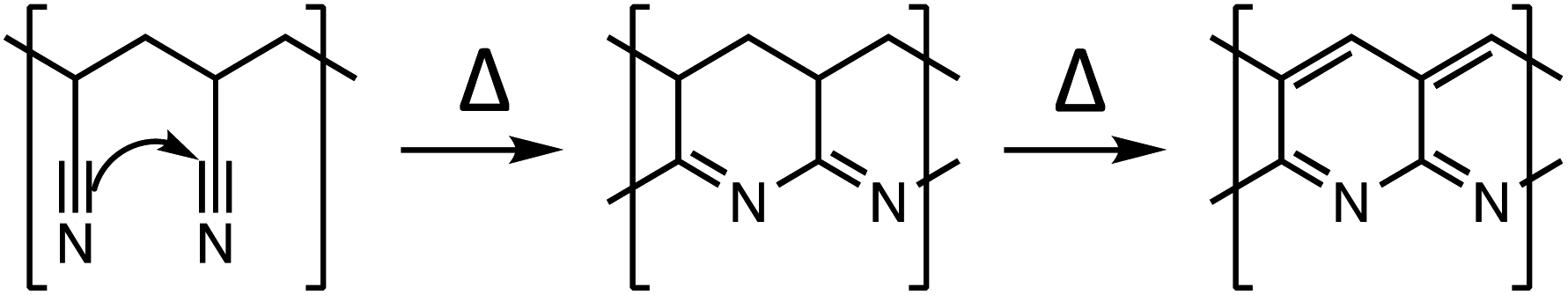 | ||
| Scheme 1 Thermal cyclization of PAN. | ||
The authors attribute the formation of these conjugated structures to annealed PAN's ability to protect electrode surfaces during continuous volume changes by selectively allowing certain electrolyte components (working ions) through while providing mechanical support and, in some cases, additional electron conduction pathways. However, the reports express surprise over annealed PAN's ability to conduct ions (Li+ and Mg2+) so well and identify other unexplained electrochemical behaviors of the material, such as the large overpotential that is required to drive only the 1st lithiation of an annealed Sn/PAN electrode.16 Additionally, despite being extensively studied in the context of industrial carbon fiber production, the specific types of structural features reported in annealed PAN vary widely and are very sensitive towards the annealing conditions (temperatures, times, and presence of oxygen)17–19 and nature of the polymer (impurities from polymerization, inclusion of co-monomers, molecular weight, and stereochemistry).20–22 As such, there is a limited understanding of how the different structural features of annealed PAN influence its performance as when used as part of an electrode. Developing a fundamental understanding of those structure–property relationships would allow annealed PAN or similar materials to be further develop as effective electrode materials.
Herein we present the first systematic study of annealed PAN as a battery electrode material to understand the structural and chemical bases of its usefulness in battery anodes. Specifically, we use the time and temperature of the annealing process to tune the degree of conjugation in the PAN coatings. Targeted electrochemical experiments allow us to correlate the degree of conjugation to the onset of an electrochemical reduction response from the annealed PAN at low electrochemical potentials. The reduction reaction effectively n-dopes the polymeric matrix to allow both electronic and Li-ion conduction through the annealed PAN coatings. The results lay the groundwork for tuning the properties of PAN-containing electrodes as well as suggest a new strategy for designing similar mixed-conducting materials for use in next generation electrode materials.
Experimental
Preparation of annealed PAN electrodes
A 1 M (∼5 wt%) polyacrylonitrile (PAN) in N,N-dimethyl-formamide (DMF) solution (based on moles of monomer units) was prepared by first adding PAN powder (1.06 g, Aldrich, 181315, Lot #MKBD6325V, average Mw 150![[thin space (1/6-em)]](https://www.rsc.org/images/entities/char_2009.gif) 000) to DMF (20 mL, >99.8, DriSolv, DX1727-6, Lot #52022). The mixture was stirred with a magnetic stir-bar on a hot plate set at 80 °C for several hours until a clear and colorless solution was formed. The solution was cooled to ambient temperature before being used to spin-coat substrates.
000) to DMF (20 mL, >99.8, DriSolv, DX1727-6, Lot #52022). The mixture was stirred with a magnetic stir-bar on a hot plate set at 80 °C for several hours until a clear and colorless solution was formed. The solution was cooled to ambient temperature before being used to spin-coat substrates.
A suspension of 25 wt% Sb powder in a 10 wt% solution of PAN in DMF was prepared by first adding ball milled Sb powder (100 mg, 99.5%, Alfa Aesar, 10099, cryo ball-milled at 30 Hz for 30 minutes, 9 times) to DMF (2.7 g) and stirring with a magnetic stir-bar at ambient temperature until a homogenous suspension was formed. Powdered PAN (300 mg) was then added and the mixture stirred on a hotplate set to 80 °C for several hours until the PAN was fully dissolved. The solution was then cooled to ambient temperature before being used to spin-coat substrates.
Electrodeposited Sb@Ni electrodes were prepared by modifying a previously reported aqueous Sb deposition solution (400 mM citric acid, 25 mM Sb2O3, titrated to pH 6 with KOH).23,24 The Sb was electrodeposited onto a Ni foil (Shop-aid, Inc., Alloy 200/201, 0.001′′ thickness, >99.00% Ni, Lot #83944) masked to a 2′′ diameter circle in a 3-electrode cell. The Ni foil was positioned under a SS mesh counter electrode and was held at −1.05 V vs. a SCE reference electrode until 100 mC cm−2 of charge was passed. Circular punches of 3/8′′ diameter were taken from this deposit and used as the Sb@Ni electrodes in the following spin coatings, anneals, and electrochemical experiments.
The PAN@SS and PAN@Sb@Ni electrodes were made by spin-coating stainless-steel (SS) disks (MTI, CR2025 spacer, SS304, Φ 15.5 mm by T 0.2 mm) or Sb@Ni electrodes, respectively, with the 1 M PAN solution using a MTI VTC-100 Vacuum Spin Coater set with the following parameters: 2000 rpm for 20 seconds followed immediately by 8000 rpm for 10 seconds. The Sb/PAN@PAN@SS electrodes were made by first spin coating a SS disk with the 1 M PAN solution as before. The PAN@SS substrate was then cured on a hotplate at 100 °C for 10 minutes before being spin-coated at 8000 rpm for 120 seconds with the 25 wt% suspension of Sb powder in 10 wt% PAN solution to produce the Sb/PAN@PAN@SS electrodes.
All electrodes were annealed in a Lindberg (Model 55322-3, 2′′ OD alumina tube) tube furnace under flowing argon. The electrode to be annealed was placed in an alumina boat, placed in the center of the tube, and the tube sealed. The tube was evacuated then refilled with argon three times before argon was set to flow over the sample at 100 mL min−1. The temperature was ramped to the desired annealing temperature at the maximum ramp rate (∼50 °C min−1). The annealing time was started when the desired temperature was reached. When the annealing time was reached, the tube furnace was turned off and opened to quench the sample to ambient temperature; the sample remained under flowing argon during the cooling time.
FT-IR characterization of annealed PAN samples
Immediately after removing from the tube furnace, the FT-IR spectra of the annealed PAN@SS samples were measured by pressing the annealed PAN film onto the diamond ATR crystal of a Nicolet iS50 FT-IR spectrometer. The spectra were baselined to the low and high ends of the measurement range and to a local minimum around 1700 cm−1 present in every spectrum.Electrochemical characterization of annealed PAN electrodes
All electrodes were assembled into Li-ion coin half-cells (with a liquid electrolyte of 1 M LiPF6 in 50/50 vol% EC/DEC) in an argon filled glovebox. Briefly, the coin cell was layered in the following order: a ½′′ diameter circular punch of Li foil was placed into the negative coin cell case (MTI, CR2025 cases SS304, with polypropylene sealing gasket), 3 drops of electrolyte, 5/8′′ diameter circular punch of polypropylene separator (MTI, Li-ion battery separator film, 25 μm thick, Batch #120313), ∼50 μL of electrolyte, 3/4′′ diameter circular punch of polypropylene separator, ∼50 μL of electrolyte, working electrode (an uncoated SS disk was added to the PAN@Sb@Ni electrodes as a rigid backing), wave spring, and the positive coin cell case. The coin-cell assembly was pressed at 0.9 tons using a compact digital pressure controlled electric crimper (MTI MSK-160E). The cells were allowed to rest for at least 12 hours before any electrochemical testing.Electrochemical experiments were carried out on the coin cells using either an Arbin cycler (Model LBT20084) for the galvanostatic/potentiostatic experiments, a Gamry Interface 1010 for the electrochemical impedance spectroscopy (EIS), or a Gamry Reference 3000 potentiostat for the variable rate cyclic voltammetry (CV). The EIS was run between 300 kHz and 100 mHz with an AC excitation of 10 mV vs. OCV.
Results and discussion
Structural characterization of annealed PAN films using FT-IR
To prepare samples for annealing and subsequent characterization, PAN was first spin-coated onto stainless steel substrates (referred to as PAN@SS) and annealed under flowing argon for a set of different times and temperatures, as shown in Fig. 1. The spin-coating parameters were chosen to produce uniform films with a thickness of ∼0.5 μm, which was determined by the cross-sectional SEM image seen in ESI Fig. S1.† All of the annealed PAN films were similar in appearance, exhibiting the same opalescent bronze color regardless of annealing conditions, though they did darken slightly over several hours upon exposure to air, suggesting the produced films were reactive with oxygen or moisture. As such, all the following characterizations were done quickly to minimize the exposure of the samples to air.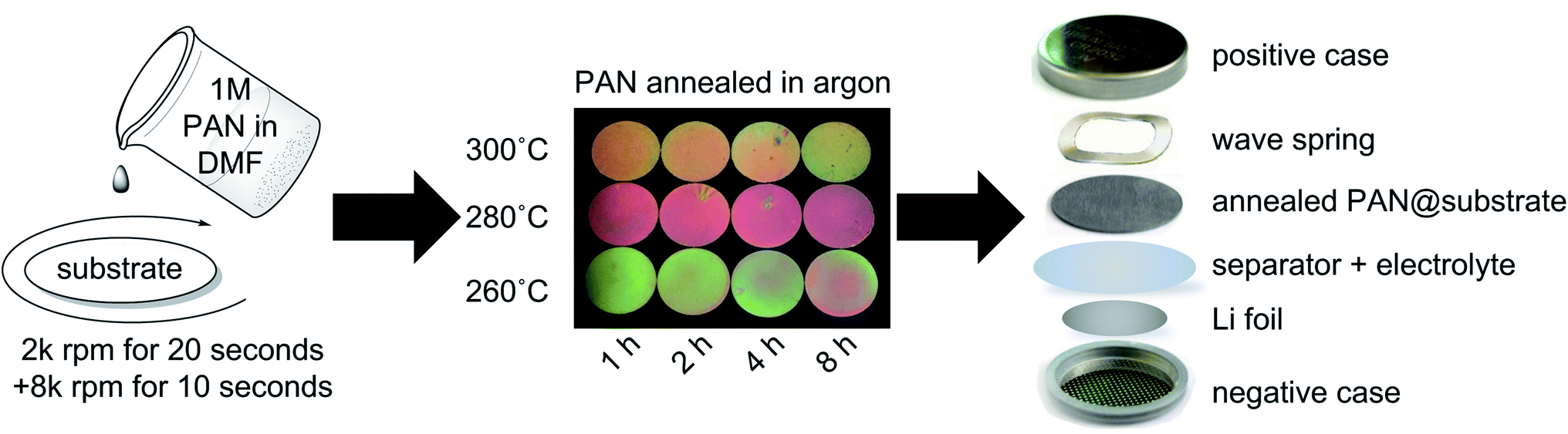 | ||
| Fig. 1 (Left) Schematic depicting the spin coating parameters for making the PAN films to be annealed. (Center) Photograph of the PAN films coated onto stainless steel (SS) substrates annealed under different conditions. (Right) Schematic depicting the use of the annealed PAN films as electrodes in lithium half-cells to study their transport properties. | ||
The annealed PAN films were first characterized with ATR FT-IR. Representative spectra of the annealed PAN films are shown in Fig. S2 in the ESI,† and they match those previously reported in literature.17,18,20,22 Upon annealing, the nitrile stretch at 2243 cm−1 disappears as a series of intense and overlapping peaks in the 1000–1800 cm−1 range appear. This spectral evolution corresponds to the reaction of adjacent nitrile groups to form fused-ring ladder conjugated structures in annealed PAN. The cyclization process is likely initiated by impurities in the PAN film, such as polymer chain terminating functional groups, or residual moisture and oxygen from the spin coating process. As depicted in ESI Fig. S2,† the ladder structure only has one conjugated imine edge, while the methylene backbone of the polymer remains fully saturated. While some previous reports suggest that fully aromatic structures (sp2 carbon only) form during the annealing, the presence of some absorption peaks around 2900 cm−1 even after annealing indicates that there is at least some sp3 carbon present in the annealed structure.
This is in contrast to PAN annealed under air, where the presence of oxygen promotes the full aromatization of fused-ring ladder structure as well as the introduction of oxygen functionality (ketone and hydroxyl groups).17,19,21,25,26 Such reactions with oxygen or moisture are likely what is occurring when the argon-annealed PAN films are exposed to air at ambient temperatures. While there is no change in the IR spectrum of the argon annealed PAN films over a few hours of air exposure, there is blending/blurring of some absorption peaks after days to weeks air exposure, suggesting aromatization and oxygen functionalization of conjugated domains occurs slowly.
Fig. 2 shows the region in the FT-IR spectra between 1000 and 1800 cm−1 for every annealing condition. For the sample annealed at 260 °C for 1 hour an absorption peak doublet is present around 1600 cm−1. We attribute the left peak at 1610 cm−1 (blue) to the presence of a secondary imine, which corresponds to the middle of a –C![[double bond, length as m-dash]](https://www.rsc.org/images/entities/char_e001.gif) N–C edge of the fused ring conjugated domain depicted. While the exact terminating functionality of the conjugated regions is not definitively known, we attribute the right peak at 1580 cm−1 (red) to a primary imine, which corresponds to the depicted –CN–H functionality that terminates a conjugated domain.22 Example structures are inlayed in Fig. 2 and are based on a qualitative comparison of the imide peak intensities. As the 1610 cm−1 (fused-ring) peak intensity increases relative to the 1580 cm−1 (terminal) peak, the length of conjugated domains likely increases. This demonstrates that the degree of conjugation in the annealed PAN films can be tuned simply by changing the annealing conditions.
N–C edge of the fused ring conjugated domain depicted. While the exact terminating functionality of the conjugated regions is not definitively known, we attribute the right peak at 1580 cm−1 (red) to a primary imine, which corresponds to the depicted –CN–H functionality that terminates a conjugated domain.22 Example structures are inlayed in Fig. 2 and are based on a qualitative comparison of the imide peak intensities. As the 1610 cm−1 (fused-ring) peak intensity increases relative to the 1580 cm−1 (terminal) peak, the length of conjugated domains likely increases. This demonstrates that the degree of conjugation in the annealed PAN films can be tuned simply by changing the annealing conditions.
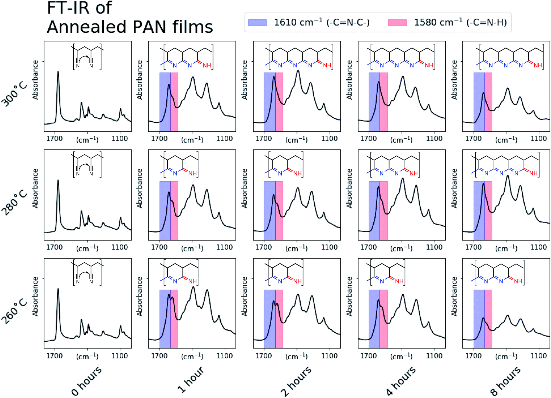 | ||
| Fig. 2 A selected area of the FT-IR spectra of PAN films annealed under every condition. We have assigned the features at 1610 cm−1 and 1580 cm−1 to secondary-imine and primary-imine functionalities, respectively. The disappearance of the peak at 1580 cm−1 corresponds well to the onset of the annealed PAN's redox activity at low electrochemical potentials. Examples of the conjugated structures we expect exist in the annealed PAN films are inlayed and their important functionalities indicated on the spectra. | ||
Electronic behavior of annealed PAN films
To assess the effect of degree of conjugation on the electronic behavior of the annealed PAN films, we first assembled the PAN@SS samples into Li-ion half-cells as depicted in Fig. 1. The half-cells serve as an electrochemical cell where electrochemical impedance spectroscopy (EIS) can be used to assess the electrochemical behavior of the annealed PAN@SS electrodes. However, initial EIS measurements of the as-assembled cells showed no observable difference between electrodes. All the annealed PAN@SS electrodes exhibit high impedance behavior similar to unannealed PAN@SS electrodes. This is likely due to the fact that the types of structures produced as a result of annealing exhibit semiconducting behavior and little electronic conductivity unless doped.27–30 This is also supported by a series of 4-point probe measurements of PAN films on glass substrates annealed under the same conditions: for every annealing condition, the conductivity of the films was too low for the 4-point probe to make a meaningful measurement. As such, we attempted to n-dope the annealed PAN films by galvanostatically sweeping the cells at 1.0 μA cm−2 to a low potential of 10 mV vs. Li/Li+. Such an n-doping reaction would involve the electrochemical reduction of a conjugated domain in the annealed PAN film by an electron supplied by the SS substrate. By necessity, the reduced conjugated domain must be charge balanced, and intercalation of a small and abundant Li+ from the liquid electrolyte is the most likely mechanism for this to happen.Fig. 3 shows the voltage profiles measured for each cell during the galvanostatic sweep. Most voltage profiles show the PAN@SS electrodes polarizing to the lower voltage cutoff of 10 mV vs. Li/Li+ with negligible capacity passed during the sweep, indicating that PAN films annealed at those conditions do not exhibit any redox activity and are not n-doped, which we attribute to their small degree of conjugation. The voltage profiles with shaded backgrounds show the abrupt onset and slight depolarization of the PAN@SS electrodes, followed by a voltage plateau at low potentials during the sweep, indicating that some electrochemical reduction reaction is occurring. We attribute the reduction to the intercalation of Li-ions into the annealed PAN film, which is analogous to the injection of an electrons (n-doping) into the conduction band of the annealed PAN film along with charge compensating Li-ions. Note that this only occurs in cells where the PAN@SS electrodes have been annealed at higher temperatures and longer times, indicating that a higher degree of conjugation in the annealed PAN films is required for this n-doping process to occur. The shape of the voltage profiles, with a slight depolarization at the beginning can be rationalized by the annealed PAN films becoming more electrically conducting upon n-doping. The films are initially relatively electrically insulating, which makes the initial Li-ion intercalation require a slight overpotential. However, upon initial n-doping of the PAN films, their electronic conductivity rises and the overpotential for continued Li-ion intercalation decreases, resulting in the slight rise in half-cell voltage during the galvanostatic sweeps despite a reducing current being continually applied.
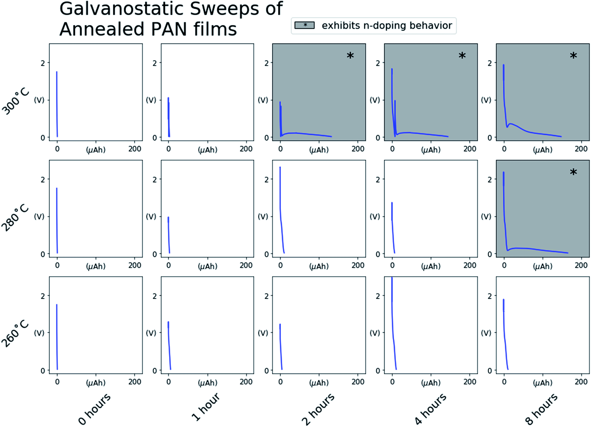 | ||
| Fig. 3 Voltage profiles obtained during the 1.0 μA cm−2 galvanostatic sweeps of PAN@SS electrodes annealed at each condition. The shaded backgrounds indicate that the PAN@SS electrodes annealed at those conditions undergo an n-doping reaction as demonstrated by the slight rise in voltage at potentials approaching 10 mV vs. Li/Li+ followed by a sloping voltage plateau. | ||
To further verify that the voltage plateaus observed in Fig. 3 correspond to n-doping of the annealed PAN films and the concomitant rise in electronic conductivity, EIS measurements of half-cells were performed after the galvanostatic sweeps. Fig. 4 shows the impedance vs. frequency for each cell before (blue trace) and after (red trace) the galvanostatic sweeps. The impedance traces of all of the PAN films before the galvanostatic sweeps are approximately the same, with low impedance values at high frequencies sloping to high impedance values at low frequencies with some subtle features. After the galvanostatic sweeps, the n-doped PAN films (*) exhibit decreased impedance values at all frequencies, with shallow plateaus at both the low and high frequencies. The shapes of these impedance spectra match that of an uncoated and electrically conducting SS electrode (ESI Fig. S3†), indicating that the n-doped PAN films also exhibit electrically conducting behavior similar to a bare metallic electrode. The low impedance values at the high frequency end of the spectra are a result of the PAN films' electronically conducting behavior, while the higher impedance plateau at the low frequency side of the spectra are dominated by the ionic behavior of the liquid electrolyte at the electrode surface.
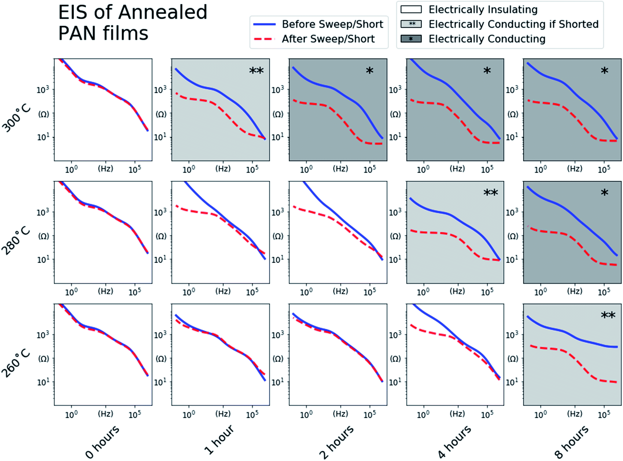 | ||
| Fig. 4 Impedance values measured using EIS of the PAN films annealed at every condition before the galvanostatic sweeps of their half-cells (blue) and after the galvanostatic sweeps or an additional 24 hour 0.01 V potentiostatic “short” (red). The EIS spectra with shaded backgrounds indicate that the behavior of the PAN film annealed under those conditions as either electrically conducting after the galvanostatic sweep (*), or electrically conducting after an additional 24 hour potentiostatic “short” (**). | ||
It was noted that replicate PAN@SS electrodes annealed at some conditions (280 °C, 4 hours) exhibited different behaviors during the galvanostatic sweep depending on the applied current density, sometimes exhibiting redox inactivity and sometimes becoming n-doped. This suggests that under those specific annealing conditions, the PAN films were near the threshold of the degree of conjugation required to see one behavior versus the other. In such threshold samples, a galvanostatic sweep at a high current density may reach the cutoff voltage limit of 0.01 V vs. Li/Li+ before the PAN film becomes n-doped, while a galvanostatic sweep at a lower current density would successfully n-dope the PAN film before the voltage cutoff was reached.
To ensure that n-doping of these threshold samples occurs if possible, all of the half-cells indicating no redox activity during the sweep were “shorted” by holding the voltage at 0.01 V vs. Li/Li+ for 24 hours. The impedance of the “shorted” cells was remeasured, and in some cases exhibited the impedance behavior of the n-doped PAN films. These threshold samples are identified in Fig. 4 (**). The samples with the unshaded backgrounds are those that exhibited the same impedance behavior before and after the “short”, identifying PAN films annealed under those conditions as insufficiently conjugated to become n-doped.
To verify that annealed PAN films exhibiting electronic conductivity after n-doping are relevant for use as binders or coatings in battery electrodes, we fabricated an electrode depicted in Fig. 5 (top). This electrode is designed to use the Sb only as an electrochemical marker in the testing of the annealed PAN's conductivity properties, and thus, thoroughly characterizing the loading and cycling performance of the Sb is beyond the scope of the discussed experiment. We chose to use Sb as an active material because it reversibly lithiates at ∼1 V vs. Li/Li+, which is sufficiently positive to be distinct from the n-doping of PAN near 10 mV vs. Li/Li+. The ball-milled Sb powder is suspended in a PAN layer that is isolated from the SS substrate by a PAN-only layer, to form a Sb/PAN@PAN@SS electrode. This ensures that to see reversible lithiation of the Sb, electrons have to conduct through the annealed PAN. We chose to anneal this electrode at 280 °C for 4 hours so it would exhibit the threshold electrically conductive behavior, requiring it to be “shorted” to be n-doped and become electrically conducting.
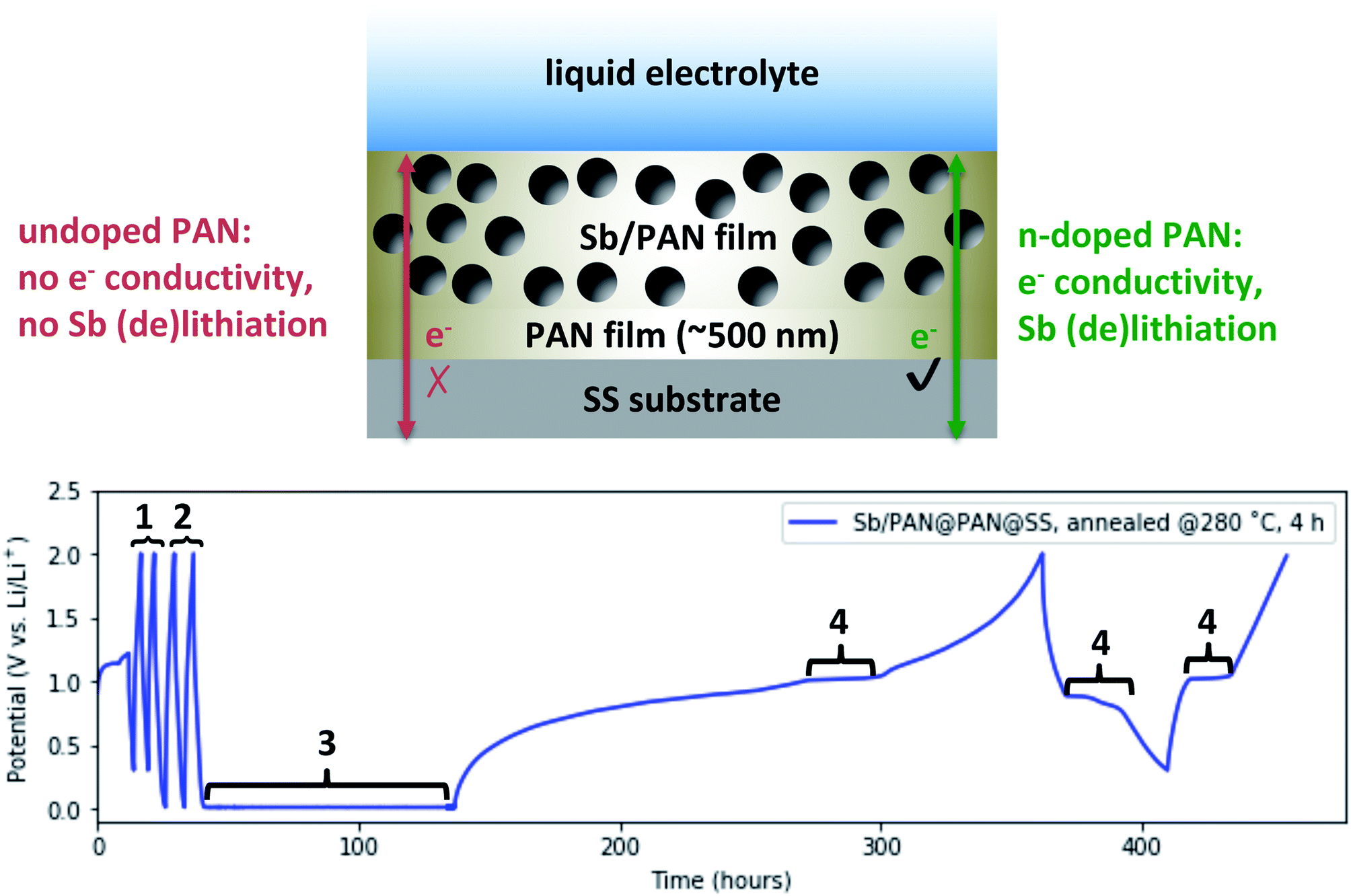 | ||
| Fig. 5 (Top) Schematic depicting an Sb/PAN@PAN@SS electrode designed to demonstrate the “doping” of and subsequent electrical conduction in annealed PAN films. (Bottom) Voltage profile obtained from galvanostatic/potentiostatic cycling of the annealed Sb/PAN@PAN@SS electrode in a lithium half-cell. Galvanostatic cycles at 1 μA cm−2 between 0.3 and 2 V vs. Li/Li+ (1) and between 0.01 and 2 V vs. Li/Li+ (2) show no Sb (de)lithiation activity. A potentiostatic hold at 0.01 V vs. Li/Li+ (3) n-dopes the annealed PAN so that the following galvanostatic cycles at 1 μA cm−2 between 0.3 and 2 V show Sb (de)lithiation activity (4). | ||
The electrode was assembled into the same Li-ion half-cell configuration as before and Fig. 5 (bottom) shows its voltage profile during a series of tests. The cell was first cycled at 1 μA cm−2 between 2 and 0.3 V vs. Li/Li+ (denoted by #1). The Sb (de)lithiation potential falls within this range, though the n-doping of the annealed PAN does not. The absence of any voltage plateaus in the ∼1 V range indicate the Sb is not lithiating, and the annealed PAN is not electrically conducting. These cycles are followed by galvanostatic cycles at 1 μA cm−2 between 2 and 0.01 V vs. Li/Li+ (denoted by #2), which now includes the potential at which the annealed PAN could become n-doped. However, because the annealing conditions were chosen to produce PAN films near the threshold to be n-doped, the PAN remains non-conducting and no Sb lithiation is observed. To n-dope the PAN, the cell is potentiostatically “shorted” at 10 mV vs. Li/Li+ (denoted by #3). The current was monitored during this step (not shown) and rose to −10 μA before dropping back to <1 μA, indicating the n-doping of the annealed PAN. The cell was then again galvanostatically cycled at 1 μA cm−2 between 2 and 0.3 V vs. Li/Li+. During the initial sweep back to 2 V, the voltage shows a shallow sloping profile, suggesting that some of the Li that intercalated into the annealed PAN is now de-intercalating. There is also a distinctly flat plateau at ∼1 V that corresponds to the delithiation of Sb, indicating that during the “shorting” process, the PAN became n-doped and electrically conducting, thus allowing the Sb to also be lithiated. On subsequent cycles between 2 and 0.3 V vs. Li/Li+, there are additional flat plateaus at ∼0.9 V then at ∼1 V vs. Li/Li+ (denoted by #4), corresponding to Sb lithiation then delithiation, showing that annealed PAN still exhibits electron conductivity even after significant amounts of Li de-intercalation. The behavior displayed in Fig. 5 is reproducible for different annealing conditions and n-doping procedures (galvanostatically or potentiostatically) given that the PAN film is sufficiently annealed to become n-doped.
Ionic transport in annealed PAN films
To measure the effect of annealing condition and degree of conjugation on mass transport through the annealed PAN films, we fabricated another Sb-containing electrode that is depicted in Fig. 6A. The electrode was fabricated by first electrodepositing a thin layer of Sb onto a Ni metal substrate. Electrodeposition ensures the Sb is well electrically connected to the current collector, and the film was kept thin enough to minimize mechanical degradation during (de)lithiation. A layer of PAN was then spin-coated onto the Sb layer as before, and the entire electrode annealed. The architecture requires that Li-ions conduct through the PAN layer in order (de)lithiate the Sb layer, thus allowing us to probe the diffusivity through the annealed PAN layer. Several of these electrodes were made and annealed at 280 °C for 1, 2, 4, and 8 hours to include annealing conditions that produce annealed PAN films with insulating, threshold, and conducting electrical behaviors. The Li-ion diffusivity in the annealed PAN layers was assessed using variable rate cyclic voltammetry (CV).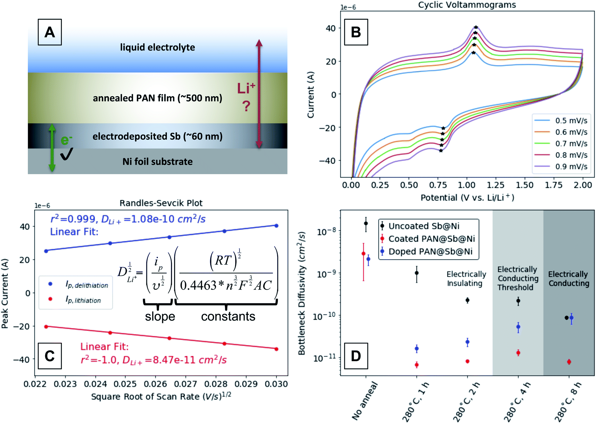 | ||
| Fig. 6 (A) Schematic depicting a PAN@Sb@Ni electrode designed to quantify the mass transport limitations through annealed PAN films. (B) Representative variable rate cyclic voltammograms of an annealed n-doped PAN@Sb@Ni electrode assembled into a lithium half-cell. The cyclic voltammograms for all electrodes annealed @ 280 °C can be found in ESI Fig. S4–S19.† (C) A representative Randles–Sevcik plot that uses the CV peak current values marked with stars. (D) Bottleneck diffusivity values determined from the Randles–Sevcik plots derived from the Sb@Ni and PAN@Sb@Ni electrodes annealed at 280 °C for various times (all values shown in ESI Fig. S20†). | ||
Example CVs between 2 and 0.01 V vs. Li/Li+ are shown in Fig. 6B, where the peak currents corresponding to reversible (de)lithiation are marked with stars. We attribute the reduction peak around ∼0.5 V to a binary Sb–Ni phase formed during annealing that lithiates at a slightly lower potential than the marked peak ∼0.8 V. During a CV in most electrochemical cells, peaks occur in the current response because the rate of the associated reaction exceeds the transport of the redox reactant to the electrode surface and a reactant concentration gradient forms. In simple systems, such as a dissolved redox active species interacting with an inert metal electrode, the Randles–Sevcik relationship relates the peak current values (ip, A) and the scan rate (ν, V s−1) to the diffusivity of the electroactive reactant.31 In more complex systems such as the PAN@Sb@Ni electrode depicted in Fig. 6A, rate limiting concentration gradients can form in the Sb film, the PAN layer, and the liquid electrolyte. Thus, the peak current values measured during a CV of such a system would result from a convolution of the ion transport in each of those layers, with the layer of the lowest ion diffusivity dominating the peak current response. As a result, the diffusivity values calculated using the Randles–Sevcik equation in Fig. 6C are semi-quantitative “bottleneck diffusivities” for the entire electrode, rather than representing intrinsic material properties. Fig. 6C demonstrates such a calculation by plotting the peak current values from the CVs in Fig. 6Bvs. the square root of the scan rate to show a linear relationship. The slope of the linear fit (ip/ν1/2) of those peak current values is proportional to the bottleneck ion diffusivity (D, cm2 s−1), where R is the gas constant (J K−1 mol−1), T is the temperature (K), n is the number of electrons in redox process (1 for 1e− + Li+ + 1/3Sb → 1/3Li3Sb), F is Faraday's constant (C mol−1), A is the area of the electrode (cm2), and C is the concentration (mol cm−3).
Fig. 6D shows bottleneck diffusivities calculated from variable rate CVs on half-cells with PAN@Sb@Ni electrodes annealed at 280 °C for 1, 2, 4, and 8 hours. We chose to use the reduction peak current around ∼0.8 V rather than ∼0.5 V for the diffusivity calculations due to its presence in all samples (including unannealed) and its greater prominence and ease of identification. Uncoated Sb@Ni electrodes were annealed under the same sets of conditions as control samples. For any given annealing condition, the bottleneck diffusivity is always greater for the uncoated Sb@Ni control electrodes compared to the corresponding PAN@Sb@Ni electrodes. This demonstrates that the calculated bottleneck diffusivity values are dominated by Li-ion diffusion through the annealed PAN layer rather than in the Sb layer. Each data point is the bottleneck diffusivity average of 3 consecutive sets of CVs on a single electrode, which verifies the electrode components are stable and give reproducible measurements (complete CV data can be found in ESI Fig. S4–S19†). The error bars are the standard deviation of the 3 consecutive measurements. The background shading of the plot indicates the expected electronic behavior of the n-doped PAN films for each of the listed annealing conditions.
The bottleneck diffusivity values for the uncoated Sb@Ni controls are shown in black. In the unannealed sample, the diffusivity value is highest (>10−8 cm2 s−1) and is likely dominated by diffusion of Li-ions in the Sb film. Upon annealing the uncoated Sb@Ni controls, the diffusivity drops to ≤10−9 cm2 s−1 for the 1, 2, and 4 hour anneals and finally down to ∼10−10 cm2 s−1 for the 8 hour anneal. The decrease in diffusivity values with longer annealing times could be due to an increase in the crystallinity of the Sb layer or the formation of Ni–Sb intermetallic phases. Powder X-ray diffraction of the electrodes was unable to confirm either possibility, as the films were too thin to give sufficient diffraction signals. Regardless, measurements of these uncoated electrodes serve as empirical controls for diffusivity measurements of the PAN coated electrodes. Diffusivity measurements for the PAN@Sb@Ni electrodes are shown in red. It should be noted that the CVs for these electrodes start and end at 2 V vs. Li/Li+, so the annealed PAN films can be considered to be undoped. While the unannealed PAN@Sb@Ni electrode exhibits only a slightly lower bottleneck diffusivity than the uncoated Sb@Ni electrode, the annealed PAN@Sb@Ni electrodes all exhibit bottleneck diffusivities ∼10−11 cm2 s−1, regardless of the annealing time. Before annealing, the PAN layer likely swells in the liquid electrolyte to form a gel that exhibits fast and near-liquid ion transport.32–35 After annealing, the PAN films are significantly cross-linked and rigid (when nitrile groups on different polymer chains cyclize together),16 likely limiting electrolyte penetration of the film and resulting in bottleneck diffusivities that are comparatively low.
The PAN@Sb@Ni electrodes only begin to exhibit annealing-time-dependent diffusivity values once the annealed PAN layers have a chance to become n-doped (Fig. 6D, blue data). Each of the PAN@Sb@Ni electrodes was held at 0.01 V vs. Li/Li+ for 48 hours to provide opportunity for the annealed PAN layer to become n-doped. The variable rate CVs were then run starting and ending at 0.01 V vs. Li/Li+. The PAN@Sb@Ni electrodes annealed for 1 and 2 hours did not show a substantial increase in ion diffusivity after this “doping” step, likely because those annealing times are insufficient to produce large enough conjugated domains in the PAN layers to become n-doped. In contrast, the electrodes annealed for 4 and 8 hours exhibit more substantial increases of ion diffusivity after the “doping” step, likely because the PAN layers in these electrodes are sufficiently conjugated to become n-doped. We attribute the increase in ion diffusivity after the n-doping of the PAN layer to the delocalization of the Li counter-anion charge over large conjugated domains. Previous studies on other systems demonstrate that the polarizability of a conjugated domain generally increases with the size of the domain,36,37 with greater polarizability leading to higher ionic conductivities.38 This is analogous to “lattice softening” in inorganic electrolytes where small non-polarizable halide ions can be substituted with larger more polarizable ions to increase ion diffusivity in the electrolyte.39 Thus, the n-doping of the large conjugated domains results in a polarizable matrix that increases the ion diffusivity compared to an undoped layer.
It is interesting to note that for the electrodes annealed for 4 hours the diffusivity of the n-doped PAN@Sb@Ni is still less than the uncoated Sb@Ni control, indicating the PAN layer is still the layer of lowest ion diffusivity in the electrode. This is in contrast to the electrodes annealed for 8 hours, where the diffusivity of the n-doped PAN@Sb@Ni electrode matches that of the uncoated Sb@Ni control at ∼10−10 cm2 s−1. This suggests that the diffusivity in the PAN layer could exceed the measured value, because Sb layer has become the layer that dominates the measured bottleneck diffusivity. Again, we attribute the increased ion diffusivity in the n-doped PAN layer to the greater extent of charge delocalization in conjugated domains that have grown in size with increased annealing time. However, additional studies are needed to definitively verify the mechanism that we propose.
Activation of mixed-conducting battery material through n-doping of conjugated domains
In this study we have shown that PAN can be annealed to such a degree that it becomes conjugated enough to be n-doped at very reducing electrochemical potentials. The n-doping effectively allows the annealed PAN to become a mixed conducting electrode coating/binder, being able to conduct both electrons and ions. Impressively, it seems possible that this n-doping reaction that activates the mixed-conducting property is possible even without the presence a liquid electrolyte16 or other salt. We hypothesize that counter anions that mediate ion conductivity in annealed PAN are the conjugated domains that have been n-doped by the electrode. The n-doped conjugated domains could result in high Li-ion diffusivity through annealed PAN by delocalizing the charge compensating anion in highly polarizable domains. This effect would not be exclusive to Li-ions and should, in principle, apply to any ion that might want to be conducting in a battery system (Na+, K+, Ca2+, Zn2+, Al3+), including those that are multivalent such as Mg2+.15 The general principle of n-doping conjugated domains to make mixed-conducting materials should also apply beyond annealed PAN. Any polymer or matrix with conjugated domains of sufficient size to be reduced within the desired electrochemical window might also be useful as mixed-conducting binders or electrode coatings. We believe additional studies towards these ends are warranted.Conclusions
In summary, we have developed a fundamental understanding of how annealed PAN films have benefited the performance of next generation electrode materials for rechargeable batteries. The formation of conjugated domains in annealed PAN films was monitored using FT-IR and can be easily controlled by simply changing the annealing time or temperature. If a PAN film is annealed to created conjugated domains of sufficient size, it can be n-doped at low potentials, where electrons from an electrode are delocalized into its conjugated domains with the concomitant intercalation of cations. The n-doping process provides additional electronic conduction pathways in battery electrodes, while the delocalization of negative charges in the conjugated domains may assist in fast ion conduction through the annealed PAN films. These results not only help to clarify why annealed PAN provides such beneficial properties for electrode materials in recent reports, but they also suggest that n-doping materials with conjugated domains is a viable strategy for making mixed-conducting binders/coatings as next generation electrode materials.Funding
This work was supported through the NSF SSMC program (SSMC-1710672).Data availability
The cyclic voltamogram data used to generate Fig. 6 can be found in the ESI.† All other FT-IR spectral raw data, EIS spectral raw data, or other electrochemical raw data are available from the authors upon reasonable request.Author contributions
Maxwell C. Schulze is the researcher that conceived the research idea, carried out the experiments, and wrote the paper with discussion, editing, and support from the principal investigator Amy L. Prieto.Conflicts of interest
There are no conflicts to declare.Acknowledgements
The authors thank Prof. Amber Krummel (CSU Chemistry) for assistance in interpreting FT-IR data. Dr Jacob Schneider (CSU Chemistry) and Prof. Annalise Maughan (CSM) also contributed to invaluable discussions and feedback useful for this work.Notes and references
- D. Bresser, K. Hosoi, D. Howell, H. Li, H. Zeisel, K. Amine and S. Passerini, J. Power Sources, 2018, 382, 176–178 CrossRef CAS.
- T. M. Gür, Energy Environ. Sci., 2018, 11, 2696–2767 RSC.
- M. Winter, B. Barnett and K. Xu, J. Chem. Educ., 2018, 23, 11433–11456 Search PubMed.
- M. N. Obrovac and V. L. Chevrier, Chem. Rev., 2014, 114, 11444–11502 CrossRef CAS.
- J. W. Choi and D. Aurbach, Nat. Rev. Mater., 2016, 1, 16013–16017 CrossRef CAS.
- J. Meng, H. Guo, C. Niu, Y. Zhao, L. Xu, Q. Li and L. Mai, Joule, 2017, 1, 522–547 CrossRef CAS.
- Y. Zhao, P. Stein, Y. Bai, M. Al-Siraj, Y. Yang and B.-X. Xu, J. Power Sources, 2019, 413, 259–283 CrossRef CAS.
- M. R. Palacin and A. de Guibert, Science, 2016, 351, 1253292 CrossRef CAS PubMed.
- J. Lang, Y. Long, J. Qu, X. Luo, H. Wei, K. Huang, H. Zhang, L. Qi, Q. Zhang, Z. Li and H. Wu, Energy Storage Mater., 2019, 16, 85–90 CrossRef.
- Y. Liu, D. Lin, P. Y. Yuen, K. Liu, J. Xie, R. H. Dauskardt and Y. Cui, Adv. Mater., 2017, 29, 1605531–1605538 CrossRef PubMed.
- F. Zheng, M. Kotobuki, S. Song, M. O. Lai and L. Lu, J. Power Sources, 2018, 389, 198–213 CrossRef CAS.
- H. Zhang, C. Li, M. Piszcz, E. Coya, T. Rojo, L. M. Rodriguez-Martinez, M. Armand and Z. Zhou, Chem. Soc. Rev., 2017, 46, 797–815 RSC.
- A. Heist, D. M. Piper, T. Evans, S. C. Kim, S. S. Han, K. H. Oh and S.-H. Lee, J. Electrochem. Soc., 2018, 165, A244–A250 CrossRef CAS.
- D. M. Piper, T. A. Yersak, S. B. Son, S. C. Kim, C. S. Kang, K. H. Oh, C. Ban, A. C. Dillon and S.-H. Lee, Adv. Energy Mater., 2013, 3, 697–702 CrossRef CAS.
- S. B. Son, T. Gao, S. P. Harvey, K. X. Steirer, A. Stokes, A. Norman, C. Wang, A. Cresce, K. Xu and C. Ban, Nat. Chem., 2018, 10, 532–539 CrossRef CAS.
- N. A. Dunlap, J. Kim, K. H. Oh and S.-H. Lee, J. Electrochem. Soc., 2019, 166, A915–A922 CrossRef CAS.
- S. Xiao, B. Wang, C. Zhao, L. Xu and B. Chen, J. Appl. Polym. Sci., 2013, 127, 2332–2338 CrossRef CAS.
- T. J. Xue, M. A. McKinney and C. A. Wilkie, Polym. Degrad. Stab., 1997, 58, 193–202 CrossRef CAS.
- Z. Bashir, Electrochim. Acta, 1991, 29, 1081–1090 CAS.
- Q. Ouyang, L. Cheng, H. Wang and K. Li, Polym. Degrad. Stab., 2008, 93, 1415–1421 CrossRef CAS.
- I. Shimada, T. Takahagi, M. Fukuhara, K. Morita and A. Ishitani, J. Polym. Sci., Part A: Polym. Chem., 1986, 24, 1989–1995 CrossRef CAS.
- N. Grassie and R. McGuchan, Eur. Polym. J., 1971, 7, 1357–1371 CrossRef CAS.
- J. M. Mosby and A. L. Prieto, J. Am. Chem. Soc., 2008, 130, 10656–10661 CrossRef CAS.
- M. C. Schulze, R. K. Schulze and A. L. Prieto, J. Mater. Chem. A, 2018, 6, 12708–12717 RSC.
- Y. Xue, J. Liu and J. Liang, J. Appl. Polym. Sci., 2013, 127, 237–245 CrossRef CAS.
- W. Watt and W. Johnson, Nature, 1975, 257, 210–212 CrossRef CAS.
- M. Suzuki, K. Takahashi and S. Mitani, Jpn. J. Appl. Phys., 1975, 14, 741–746 CrossRef CAS.
- M. H. Whangbo, R. Hoffmann and R. B. Woodward, Proc. R. Soc. London, Ser. A, 1979, 366, 23–46 CAS.
- J. J. Ritsko, G. Crecelius and J. Fink, Phys. Rev. B: Condens. Matter Mater. Phys., 1983, 27, 2612–2614 CrossRef CAS.
- T. C. Chung, Y. Schlesinger, S. Etemad, A. G. Macdiarmid and A. J. Heeger, J. Polym. Sci., Polym. Phys. Ed., 1984, 22, 1239–1246 CrossRef CAS.
- L. R. Faulkner and A. J. Bard, Electrochemical methods: fundamentals and applications, John Wiley and Sons, Hoboken, NJ, 2nd edn, 2002 Search PubMed.
- P. Hu, J. Chai, Y. Duan, Z. Liu, G. Cui and L. Chen, J. Mater. Chem. A, 2016, 4, 10070–10083 RSC.
- H. Akashi, K. Sekai and K. Tanaka, Electrochim. Acta, 1998, 43, 1193–1197 CrossRef CAS.
- K. M. Abraham, H. S. Choe and D. Pasquariello, Electrochim. Acta, 1998, 43, 2399–2412 CrossRef CAS.
- H. S. Choe, B. G. Carroll, D. M. Pasquariello and K. M. Abraham, Chem. Mater., 1997, 9, 369–379 CrossRef CAS.
- M. T. Zhao, B. P. Singh and P. N. Prasad, J. Chem. Phys., 1988, 89, 5535–5541 CrossRef CAS.
- M. Gussoni, M. Rui and G. Zerbi, J. Mol. Struct., 1998, 447, 163–215 CrossRef CAS.
- T. Takahashi, K. Nagagiri, Y. Iwadate, F. Utsuno, H. Yamaguchi and T. Ohkubo, Chem. Phys. Lett., 2018, 698, 234–239 CrossRef CAS.
- M. A. Kraft, S. P. Culver, M. Calderon, F. Böcher, T. Krauskopf, A. Senyshyn, C. Dietrich, A. Zevalkink, J. Janek and W. G. Zeier, J. Am. Chem. Soc., 2017, 139, 10909–10918 CrossRef CAS.
Footnote |
| † Electronic supplementary information (ESI) available: Additional figures depicting an SEM image, representative FT-IR and EIS spectra, and complete CV data. See DOI: 10.1039/d1sc02350k |
| This journal is © The Royal Society of Chemistry 2022 |