
 Open Access Article
 This Open Access Article is licensed under a Creative Commons Attribution-Non Commercial 3.0 Unported Licence
The influence of saccharin adsorption on NiFe alloy film growth mechanisms during electrodeposition
Anna Kotelnikova *a,
Tatiana Zubara,
Tatiana Vershininabc,
Maria Panasyuka,
Oleg Kanafyeva,
Vladimir Fedkina,
Ilya Kubasovd,
Andrei Turutind,
Sergei Trukhanovad,
Daria Tishkevichad,
Valery Fedosyuka and
Alex Trukhanovad
*a,
Tatiana Zubara,
Tatiana Vershininabc,
Maria Panasyuka,
Oleg Kanafyeva,
Vladimir Fedkina,
Ilya Kubasovd,
Andrei Turutind,
Sergei Trukhanovad,
Daria Tishkevichad,
Valery Fedosyuka and
Alex Trukhanovad
aScientific-Practical Materials Research Centre of National Academy of Sciences of Belarus, 220072 Minsk, Belarus. E-mail: anna.kotelnikova.98@mail.ru
bJoint Institute for Nuclear Research, 141980 Dubna, Russia
cDubna State University, 141980 Dubna, Russia
dNational University of Science and Technology MISiS, 119049, Moscow, Russia
First published on 14th December 2022
Abstract
This article deals with the effects of current modes on saccharin adsorption during NiFe electrodeposition, and, as a consequence, its effect on chemical composition, crystal structure, and microstructure of deposited films. For this purpose, we obtained NiFe films using direct, pulse, and pulse-reverse electrodeposition modes. The deposit composition, crystal structure, and surface microstructure are studied. Direct current (DC) and pulse current (PC) films have a smooth surface, while a pulse-reverse current (PRC) film surface is covered by a volumetric cauliflower-like microstructure. The mechanism of the film surface development was considered from the point of view of saccharin adsorption and its action as an inhibitor of vertical grain growth during different current modes. During the DC and PC modes, saccharin is freely adsorbed on the growth centers and restrains their vertical growth. Whereas in the case of the PRC electrodeposition, saccharin adsorbs during cathodic pulses and desorbs during anodic pulses. Therefore, its inhibiting action decreases, vertical grain growth rises, and a rougher surface develops.
Introduction
NiFe alloys are widely used in microelectronics as they are magnetically soft materials.1–7 The most common and best understood alloy is Permalloy, a NiFe alloy of about 79–82% concentration in Ni. Permalloy has a saturation flux density of over 1 T that can be maintained at frequencies above 100 MHz. Permalloy also has a relatively high Curie temperature (500–520 °C) and only a 10% reduction in saturation flux density at 130 °C. It's magnetoresistance coefficient ranges from 2% to 4% (2% for fields of the order of 3.75 Oe, or 300 A m−1).8NiFe alloys are extensively used as functional magnetic materials in magnetic recording media,9–11 magnetic field sensors,12–15 magnetic proximity effect,16,17 spin Hall effect,18–21 magnetic flux shields,22–25 etc. The electrical, magnetic, and mechanical properties of the NiFe precipitates are determined by their chemical composition and crystalline structure. Thus, the targeted formation of the NiFe alloys with predicted functional characteristics requires the establishment of the formation conditions influence on the structure and properties of the obtained films.
The contemporary level of technical development allows engineers to get closer to the minimum size of the objects intended for electronics, aerospace industries, instrument manufacturing, and power engineering. Metal electrodeposition is one of the methods used to synthesize nano- and microdimensional films.26–35 Electrodeposition is an electrochemical process that allows the preparation of solid deposits of a wide range of thicknesses27,36–42 on the surface of conductive materials. It is a highly commercially relevant process, providing the basis for many industrial applications, such as electrowinning, refining, and metal plating. Electrodeposition combines low costs with high deposition rate and the ability to cover large complex surfaces.43–45
The variation of technological parameters and composition of the electrolyte ensures a controlled influence on the process of electrodeposition films and the obtaining of deposits with the assigned composition, crystal structure, and properties. Pulse current (PC) electrodeposition has been known to produce sediments with a higher content of Fe and a lower grain size as compared to direct current (DC) electrodeposition.46–48 Applying pulse-reverse current (PRC) waveforms lead to different changes in composition and microstructure for various alloys. For example, PRC deposits of Cu and Zn have a smooth surface with a lower grain size as compared to their DC analogues,36 whereas Ni PRC deposits have a rough surface with volumetric microstructures.49 Wasekar et al.49 and Yu et al.50 in their researches connected the differences in the DC, PC, and PRC sample microstructures with the brightening agent – saccharin, which is common used to inhibit grains columnar growth.51 They assumed that saccharin adsorbs in various ways during different electrodeposition modes. But the mechanism for the formation of different microstructures has not been proposed.
Our previous studies have demonstrated the possibility of changing the magnetic properties of structures based on the NiFe alloy (including the shielding efficiency) by changing the synthesis conditions, chemical composition, microstructure and subsequent thermal processing of products.7,22,42,52 Understanding the mechanism of the PRC electrodeposition mode effect on the NiFe films surface microstructure would expand the possibilities of targeted synthesis of structures with desired characteristics.
The aim of our current research was to investigate the influence of the electrolyte additive saccharin on the mechanism of NiFe alloy grain growth in direct, pulse, and pulse-reverse electrodeposition modes. We assumed that saccharin adsorbs on the film surface differently during alternant cathodic–anodic current action in comparison with it's behavior during cathodic current action. Therefore, we formed NiFe films in DC, PC, and PRC modes and studied their composition, crystal structure, and surface microstructure. As a result, a mechanism of saccharin adsorption–desorption and grain growth was proposed.
Experimental
The electrodeposition method was used to obtain NiFe films. The process scheme is presented in Fig. 1a. The substrates for the electrodeposition were polished steel plates. The plate length and width were 40 mm. To provide electrodeposition on one side of the plate, the other side was isolated. Polished steel was chosen as it provides easy separation of the films from the substrates for further investigations.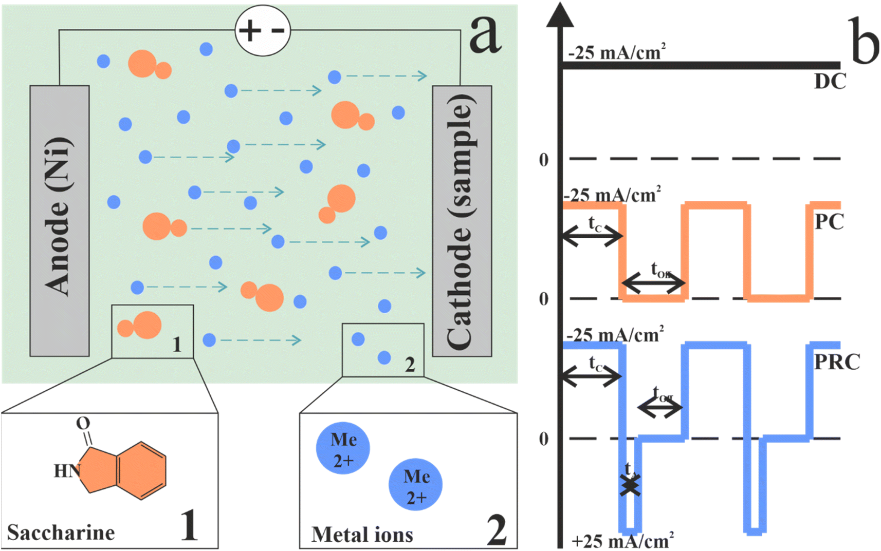 | ||
| Fig. 1 A schematic representation of the electrolytic deposition circuit (a) and the scheme of direct, pulse, and pulse-reverse electrodeposition current waveforms (b). | ||
The NiFe films were deposited from a complex electrolyte containing NiSO4·7H2O—210 g L−1, NiCl2·6H2O—20 g L−1, FeSO4·7H2O—15 g L−1, H3BO3—30 g L−1, MgSO4·7H2O—60 g L−1, Rochelle salt KNaC4H4O6·4H2O—30 g L−1, ascorbic acid C6H7O6—2 g L−1, and saccharin C7H5NO3S—2 g L−1. The electrolyte volume was 20 L. The electrolyte was mixed with an air compressor during the films electrodeposition.
During the electrodeposition process, metal cations are reduced to neutral atoms and deposited on the cathode surface. Nickel and iron sulphates are the sources of nickel and iron cations. These salts are available, not expensive, and highly soluble in water. Nickel chloride was used as a source of nickel cations and chloride anions. The presence of chloride ions increases the electrolyte conductivity and prevents Ni anode passivation (which is a frequent problem for electrolytes with high Ni salt concentrations).53
Boric acid was added as a buffer additive to stabilize the solution pH fluctuations (mostly related to alkalization (increase in pH) due to hydrogen evolution) and to reduce anomalous character of Ni and Fe codeposition.54,55 Magnesium sulfate was used to increase the electrolyte conductivity and electrodeposition efficiency and to perform electrodeposition with higher current densities.55,56
As a complexing agent, Rochelle salt (sodium–potassium tartrate) was used. In the absence of any complexing agent, Ni has more positive electrode potential than Fe. But in the presence of tartrate ions, both Ni and Fe cations form complex salts with close values of instability constant. Therefore, the influence of electrode potential difference on the rival electrodeposition of Ni and Fe ions was reduced. In addition to this, the binding of Fe2+ in the tartrate complex to some extent prevents its oxidation to Fe3+ and prolongs the life of the electrolyte. Ascorbic acid was taken to reduce Fe2+ oxidation to Fe3+. Saccharin was used as a brightener and vertical grain growth inhibitor to obtain films with low roughness.55,57
Such a low concentration of ferrous sulphate relative to nickel sulphate and chloride is due to the anomalous nature of coprecipitation of the NiFe alloy. It manifests itself in the formation of an alloy with a higher iron concentration than expected based on the ratio of the concentrations of metal ions in the electrolyte. For this reason, a deliberately smaller amount of iron salt is added to the electrolyte to reduce the concentration of iron in the deposited alloy. The ratio of ion concentrations in our electrolyte was c(Ni2+)![[thin space (1/6-em)]](https://www.rsc.org/images/entities/char_2009.gif) :c(Fe2+) = 15.4:1.
:c(Fe2+) = 15.4:1.
It should be noted that the control of the composition of the alloy only by changing the concentration of iron salt in the electrolyte has its drawbacks, in particular, the use of electrolytes with a very low content of iron salt is undesirable. Since during electrodeposition the electrolyte is depleted of nickel and iron ions, when thick films and coatings are deposited from electrolytes of small volume, a composition gradient is formed from the lower layers to the upper ones. Replenishment of metal ions is possible through the use of a soluble metal anode, or through the adjunction of additional amounts of salts at certain intervals of electrolyte use.
In our experiment, we used a nickel anode, the dissolution of which compensated for the loss of nickel ions. During the films electrodeposition, the content of iron ions in the electrolyte was not corrected. This solution is associated with a small value of the charge passed through the bath ratio to the volume of the bath (1120 C per L). Which, according to our previous studies,41,52,58 leads to a slight decrease in the content of iron ions in the electrolyte of a given composition.
The temperature of the electrolyte was kept at 35 °C and the pH was maintained at 2.3. The current density was 25 mA cm−2 for both cathodic and anodic current. Under these conditions, the deposition rate was around 25 μm h−1 for DC electrodeposition mode. The described electrodeposition technology allows for the production of NiFe alloy films with satisfactory mechanical and aesthetic characteristics.52,58
Current parameters are presented in Table 1 and Fig. 1b shows current waveforms for deposition modes in our experiment. A sample DC was obtained at direct current for 60 min. A sample PC was obtained in pulse mode with a pulse duration of 0.1 s for 120 min. The pause duration was equal to the pulse time. A sample PRC was obtained in pulse-reverse mode with a pulse duration of 0.1 s, reverse pulse duration of 0.005 s and pause duration was 0.095 s. The choice of these durations of the cathodic pulse and pause is related to our previous study, in which, with similar parameters, a homogeneous film was obtained that practically does not contain pores.52,58 An appropriate anode pulse duration was chosen to demonstrate the effect of even the current reversal period on the properties of the NiFe film.
| Sample | Cathodic pulse, s | Pause, s | Anodic pulse, s | Total deposition time, min | Effective deposition time, min |
|---|---|---|---|---|---|
| DC | 3600 | — | — | 60 | 60 |
| PC | 0.1 | 0.1 | — | 120 | 60 |
| PRC | 0.1 | 0.095 | 0.005 | 126 | 60 |
To deposit PC and PRC films with thicknesses close to the DC film the total deposition time tTD was calculated. This value is correct only under identical synthesis conditions, including the composition, temperature and pH of the electrolyte, current density, mixing intensity, etc.
Total deposition time for pulse-reverse mode was calculated by eqn (1):
| tTD = tED(tC + tA + toff)/(tC − tA), | (1) |
According to the films cross-section images on the optical microscope, the samples thickness was 25.4, 25.2 and 25.9 μm for DC, PC and PRC respectively.
AZtecLive Advanced with Ultim Max 40 (Oxford Instruments, Bognor Regis, UK) investigated the chemical composition using energy-dispersive X-ray spectroscopy (EDS). The crystal structure investigation was carried out by X-ray diffraction structural analysis (XRD) on an EMPYREAN (PANalytical, Malvern Instruments, Malvern, UK) powder diffractometer using Cu-Kα radiation in the Bragg–Brentano geometry, focusing in the angle range of 2θ = 40–100°. The sizes of the coherent scattering regions (CSR) were estimated using the Williamson–Hall method59,60 for all peaks from the fcc solid solution. The surface microstructure was studied using the scanning electron microscope (SEM) Zeiss EVO 10 (Zeiss, Oberkochen, Germany). Films thickness was defined from the films cross-section by optical microscope Smart 5MP PRO (Delta optical, Ontario, Canada).
Results and discussion
The percentage of iron obtained from the analysis of energy-dispersive X-ray spectra is presented in Fig. 2. There is an increase in the concentration of Fe during the transition from direct current mode (36.4 at%) to pulse current mode (42.2 at%). The reason for the increase in the Fe content is the feature of the initial stages of sedimentation. In the early stages of deposition, the widely described anomalous codeposition of iron is observed, accompanied by the formation of iron-rich layers.22,48,61–66 The pulse mode is a special case of direct current electrodeposition. It consists of repeated initial stages of a DC, which means that layers enriched with iron are formed not only at the beginning of deposition, but throughout its entire length.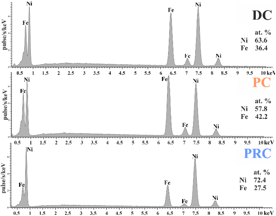 | ||
| Fig. 2 EDS patterns of NiFe films obtained by direct, pulse, and pulse-reverse electrodeposition. | ||
There is a decrease in the Fe content during the transition to pulse-reverse mode (27.5 at%). This is due to two factors. Pulse-reverse mode includes a stage of the films’ short-term dissolution when the polarity of the current is reversed. Iron has a lower electrode potential (−0.44 V) than nickel (−0.24 V), which means iron is more prone to oxidation and dissolves faster under the action of the reverse current. Nevertheless, the difference in the rates of Fe in Ni dissolution is too small for short anodic pulses and is not the main factor in our case. However, the dissolution of the iron hydroxides in the surface region has a significant contribution to reducing the anomalous character of deposition even for short anodic pulses. Therefore, the iron content in the film is reduced.67–70
Fig. 3 and Table 2 show the results of X-ray diffraction structural analysis (XRD) investigations of the NiFe films obtained by the different current modes. There is a number of well-distinguished peaks can be observed in the XRD patterns. The most intense and characteristic peaks are 42–43 deg (corresponding to the fcc lattice atomic plane (111)) and 50–51 deg (corresponding to the fcc lattice atomic plane (200)). There are also much less intense and broadened peaks corresponding to the fcc lattice atomic planes (220), (311) and (222). The peaks appropriate to the Fe bcc lattice atomic planes were not observed. This indicates that these films are formed by solid solution of Fe in Ni and have a face-centred cubic Ni lattice and the space group Fm3m (no. 225). Broadened peaks in the diffraction patterns indicate either a small crystallite size or high internal stresses in the lattice. A decrease in the integral intensity and an increase in the width at the half-height of the (111) peak were observed for the PRC sample, while there were no significant differences between the PC and DC samples. An increase in the integral intensity of the (200) peak was observed for the PRC sample. The width at the half-height of the (200) peak decreases from the DC through the PC to the PRC sample. All the samples have a predominant crystallographic orientation: one can see a change in the ratio of X-ray peaks (200) and (111). The most intense peak (111) of the fcc lattice was taken as 100%. For completely misoriented nickel powder, the ratio of the integral intensities of the atomic planes (200) and (111) is 46%, which is not observed for any of the studied samples. There is a decrease in the ratio I(200)/I(111) during the transition from direct current mode (73%) to pulse current mode (63%). The PRC sample has the biggest value of the ratio I(200)/I(111) of 95%. A comparison of our films ratio I(200)/I(111) with the one of the nickel powder indicates that in the DC, PC and PRC film, the (200) texture of the fcc structure is predominant.
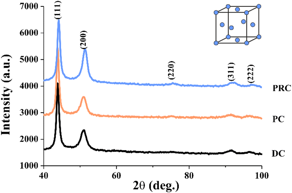 | ||
| Fig. 3 XRD patterns of NiFe films obtained by direct, pulse, and pulse-reverse electrodeposition. | ||
| Sample | CSR (coherent scattering regions), nm | I(200)/I(111) (ratio of the integral intensities (200) and (111)), % | a (unit cell parameter), nm | V (unit cell volume), nm3 |
|---|---|---|---|---|
| DC | 6 ± 1 | 73 ± 0.7 | 0.3570 ± 1 × 10⁻⁴ | 0.0455 ± 1 × 10⁻⁴ |
| PC | 7 ± 1 | 63 ± 0.6 | 0.3571 ± 1 × 10⁻⁴ | 0.0455 ± 1 × 10⁻⁴ |
| PRC | 6 ± 1 | 95 ± 0.9 | 0.3577 ± 1 × 10⁻⁴ | 0.0458 ± 1 × 10⁻⁴ |
The sizes of the coherent scattering regions (CSR) were estimated using the Williamson–Hall method for all peaks from the fcc solid solution present in the X-ray diffraction pattern. The estimates showed that the main factor responsible for the strong broadening of X-ray peaks is the small size of the CSR. Table 2 shows that sizes of the CSR (coherent scattering regions) were 6–7 nm for all samples. Crystal lattice parameters a (unit cell parameter) and V (unit cell volume) are almost the same for all films and are around 0.3570–0.3577 nm and 0.0455–0.0458 Å3 respectively.
The surface microstructure of the NiFe shielding films investigated using scanning electron microscopy (SEM) is shown in Fig. 4. There is a smooth and uniform surface with a lot of pores on the sample DC. It is known that electrodeposition process consists of not only main reaction of metal ions reduction, but also side reactions. The reduction of hydrogen cations is the predominant side reaction during the deposition from a sulphate electrolyte, however, the reduction of chloride ions which present in our electrolyte is also possible. The reduced hydrogen in the form of gas bubbles is adsorbed on the cathode surface and prevents the uniform deposition of metals, which contributes to the formation of pores. During the films electrodeposition the electrolyte was continuously agitated to prevent gas bubbles adsorption on the films surface. Nevertheless, pores still formed in the DC film.
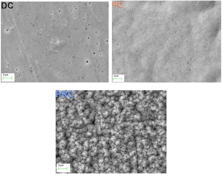 | ||
| Fig. 4 The surface microstructure of NiFe films obtained by direct, pulse, and pulse-reverse. | ||
The surface of the sample PC is also smooth and uniform and has far fewer pores. The PC electrodeposition mode is known for higher nucleation rate and further grain sizes decrease. Besides sizes of the gas bubbles formed during side reactions are much smaller in PC mode as compared to the DC mode. The higher nucleation rate in this mode results in greater uniformity and the smaller gas bubbles results in less porosity of the PC films.
The PRC film surface, on the contrary, is covered with volumetric microstructures and has many pores. Nonuniformity of the PRC film surface correlates with its increased ratio I(200)/I(111). Such a radical change in the surface microstructure, when adding even a short anodic pulse (0.005 s) to the current waveform, is caused by several reasons. First of all, passivation of the anode (sample) might occur during the anodic pulses.56,71
In the case of mechanical or salt passivation, the concentration of the dissolved metal ions increases in the anode layer and the latter becomes oversaturated with salt. Passivation is also possible due to the formation of metal oxides on the surface of the anode since the electrolyte is enriched with oxygen while stirring. Therefore, some regions (or even all the anode surface at the higher current densities) become covered by metal salt/oxide microcrystals, which reduce metal dissolution leading, to increased etching of the surface areas not covered with metal salt/oxide. This means that a relief surface can be formed. To summarize the above, the duration of the anodic pulses was too small by comparison with the cathodic pulses in our experiment, which means that the passivation effect couldn't be primary, but only secondary.
Pulse-reverse modes are known to have less overpotential. Decreasing the value of overpotential leads to a decline in the nucleation rate.49,72 Therefore, a smaller number of nuclei and a deposit with a bigger grain size are formed, in contrast to DC and PC deposits. This factor could also contribute to the development of volumetric microstructures on the sample surface.
The greatest influence on the surface microstructure was exerted by the reduced adsorption of saccharin in the pulse-reverse mode.49–51,73 Saccharin is widely used as the brightener in the nickel plating and electrodeposition of NiFe alloys as it inhibits vertical grain growth, leading to smooth and shiny deposits.74,75 Our scheme of its adsorption in cathodic (DC and PC modes) and alternant cathodic–anodic (PRC mode) current and thus different ways of alloy formation is shown in Fig. 5 and 6.
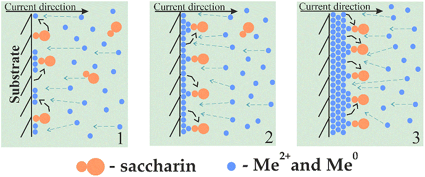 | ||
| Fig. 5 Scheme of saccharin adsorption and the NiFe film growth mechanism in direct and pulse current modes electrodeposition. | ||
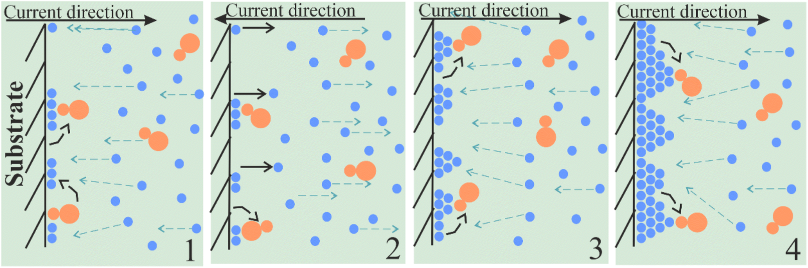 | ||
| Fig. 6 Scheme of saccharin adsorption and film growth mechanism in pulse-reverse current mode electrodeposition. | ||
Stage 1 in Fig. 5 displays the beginning of the deposition. When the cathodic current is applied, metal ions start to move to the sample surface. Their movement near the sample and deposition are complicated by an ordered adsorption layer of saccharin, which plays the role of a barrier or semipermeable membrane. Thus, metal particles are forced to settle in areas free of saccharin. However, the saccharin molecules move to the newly deposited nuclei and prevent the precipitation of further particles. Thus, the vertical growth of grains is weakened (stage 2).
In the case of cathodic current only, layer-by-layer growth of sediment occurs further, with a gradual increase in the amount of adsorbed saccharin and, consequently, even greater inhibition of vertical growth (stage 3). It results in a smooth and tight deposit formation.
Deposit growth occurs differently when cathodic and anodic currents are alternated. After the first cathodic pulse (stage 1 in Fig. 6), the anodic pulse is applied. During it, a partial dissolution of the precipitate and saccharin desorption into the electrolyte happens (stage 2). Thus, a smaller number of saccharin molecules stay adsorbed and they become unordered. Although the duration of the anode pulse is much shorter than the cathode pulse (20 times in our experiment), in pulse-reverse mode the desorption rate significantly exceeds the adsorption rate of saccharin, and thus the adsorption layer does not have time to recover. Therefore, grain vertical growth increases as the barrier effect of saccharin is reduced (stage 3). It leads to the formation of the deposit with a relief surface covered by volumetric microstructures (stage 4).
Conclusions
A set of NiFe alloy films was obtained using direct, pulse, and pulse-reverse electrodeposition. The samples thickness was 25.4, 25.2 and 25.9 μm for DC, PC and PRC respectively according to the films cross-section images. The samples had a composition of 27.5 to 42.2 at% Fe, with differences caused by changes in current modes. The PC film had a higher Fe content (42.2 at%) as compared to the DC film (36.4 at%), which was the result of more anomalous character of codeposition in PC mode. The PRC film's Fe content (27.5 at%), on the contrary, was lower than the content of the DC and PC films. The reason for this is the faster Fe oxidation and dissolution during anodic pulses. XRD studies of the crystal structure have shown that the most intense and characteristic peaks correspond to fcc lattice atomic planes for all samples. The unit cell parameter was almost the same for the DC and PC samples, but increased from 0.3571 to 0.3577 nm and from 0.0455 to 0.0458 nm3 with the transition from pulse to pulse-reverse electrodeposition. The reason for the extension of the crystal lattice could be the effect of the chemical composition. The microstructure was investigated using SEM. The DC and PC samples had a smooth surface, while the PRC sample had a surface covered by volumetric microstructures. Such a dramatic modification of the surface microstructures is due to the difference in saccharin adsorption during electrodeposition in cathodic and alternant cathodic–anodic current. In the case of DC or PC deposition, saccharin is well adsorbed at the sample surface, and it inhibits vertical grain growth. As a result, a smooth and uniform deposit forms. Whereas in PRC deposition, anodic pulses lead to faster saccharin desorption to the bulk of the electrolyte, leading to a decrement of its vertical growth inhibitor activity. Thus, grain vertical growth is increased and contributes to the development of volumetric microstructures on the deposit surface.Author contributions
Conceptualization, A. Kotelnikova, T. Zubar and A. Trukhanov; methodology, O. Kanafyev and M. Panasyuk; formal analysis, D. Tishkevich and V. Fedkin; investigation, A. Kotelnikova, T. Zubar, T. Vershinina, I. Kubasov and A. Turutin; resources, V. Fedkin; data curation, D. Tishkevich, and S. Trukhanov; writing—original draft preparation, review and editing, A. Kotelnikova and T. Zubar; visualization, M. Panasyuk; supervision, A. Trukhanov and V. Fedosyuk; project administration, V. Fedosyuk; funding acquisition, I. Kubasov and A. Turutin.Conflicts of interest
There are no conflicts to declare.Acknowledgements
The study was performed with financial support from the Russian Science Foundation (grant no. 22-19-00808, https://rscf.ru/project/22-19-00808/). The structure studies were carried out on the equipment of the Materials Science and Metallurgy Joint Use Center in the NUST MISiS with financial support from the Ministry of Education and Science of the Russian Federation (No. 075-15-2021-696) and the State Assignment (basic research, Project No. 0718-2020-0031).References
- B. Zhang, N. E. Fenineche, L. Zhu, H. Liao and C. Coddet, J. Magn. Magn. Mater., 2012, 324, 495–500 CrossRef CAS
.
- J. C. Lloyd and R. S. Smith, J. Appl. Phys., 1959, 30, S274–S275 CrossRef
- A. T. English and G. Y. Chin, J. Appl. Phys., 1967, 38, 1183–1187 CrossRef CAS
- Y. Luo, S. K. Kang, O. Jinka, M. Mason, S. A. Cordes and L. T. Romankiw, Proc. – Electron. Compon. Technol. Conf., 2014, 1782–1789 Search PubMed
- L. Vieux-Rochaz, R. Cuchet and M. H. Vaudaine, Sens. Actuators, A, 2000, 81, 53–56 CrossRef CAS
- G. Schiavone, S. Smith, J. Murray, J. G. Terry, M. P. Y. Desmulliez and A. J. Walton, IEEE Int. Conf. Microelectron. Test Struct. Proc., 2013, 13–18 Search PubMed
- T. Zubar, A. Trukhanov, D. Vinnik, K. Astapovich, D. Tishkevich, E. Kaniukov, A. Kozlovskiy, M. Zdorovets and S. Trukhanov, J. Phys. Chem. C, 2019, 123, 26957–26964 CrossRef CAS
- J. C. Mallinson, Magnetoresistive Heads, 1996 Search PubMed
- T. Osaka, T. Asahi, J. Kawaji and T. Yokoshima, Electrochim. Acta, 2005, 50, 4576–4585 CrossRef CAS
- N. Robertson, H. L. Hu and C. Tsang, IEEE Trans. Electromagn. Compat., 1997, 33, 2818–2820 CAS
- W. Peng, O. Keitel, R. H. Victora, E. Koparal and J. H. Judy, IEEE Trans. Magn., 2000, 36, 2390–2392 CrossRef CAS
- V. V. Kondalkar, X. Li, S. Yang and K. Lee, Procedia Eng., 2016, 168, 675–679 CrossRef
- W. Y. Lee, M. F. Toney and D. Mauri, IEEE Trans. Magn., 2000, 36, 381–385 CrossRef CAS
- S. Canaguier, V. Artero and M. Fontecave, Dalton Trans., 2008, 315–325 RSC
- K. Hika, L. V. Panina and K. Mohri, IEEE Trans. Magn., 1996, 32, 4594–4596 CrossRef CAS
- L. Folks and R. C. Woodward, J. Magn. Magn. Mater., 1998, 190, 28–41 CrossRef CAS
- L. J. Zhu, D. C. Ralph and R. A. Buhrman, Phys. Rev. B, 2018, 98, 1–5 Search PubMed
- H. Wu, C. H. Wan, Z. H. Yuan, X. Zhang, J. Jiang, Q. T. Zhang, Z. C. Wen and X. F. Han, Phys. Rev. B: Condens. Matter Mater. Phys., 2015, 92, 1–6 CAS
- T. Nan, S. Emori, C. T. Boone, X. Wang, T. M. Oxholm, J. G. Jones, B. M. Howe, G. J. Brown and N. X. Sun, Phys. Rev. B: Condens. Matter Mater. Phys., 2015, 91, 1–9 CrossRef
- H. Mazraati, S. Chung, A. Houshang, M. Dvornik, L. Piazza, F. Qejvanaj, S. Jiang, T. Q. Le, J. Weissenrieder and J. Åkerman, Appl. Phys. Lett., 2016, 109, 1–5 CrossRef
- T. Y. Ma, C. H. Wan, X. Wang, W. L. Yang, C. Y. Guo, C. Fang, M. K. Zhao, J. Dong, Y. Zhang and X. F. Han, Phys. Rev. B, 2020, 101, 1–6 Search PubMed
- T. Zubar, S. Grabchikov, A. Kotelnikova, E. Kaniukov, M. Kutuzau, K. Leistner, K. Nielsch, T. Vershinina, D. Tishkevich, O. Kanafyev, A. Kozlovskiy, M. Zdorovets, V. Fedosyuk and A. Trukhanov, Nanomaterials, 2021, 11, 1–13 CrossRef PubMed
- J. H. Park, J. W. Lee, H. J. Choi, W. G. Jang, T. S. Kim, D. S. Suh, H. Y. Jeong, S. Y. Chang, J. C. Roh, C. S. Yoo, K. H. Kim, C. Park and S. J. Suh, Thin Solid Films, 2019, 677, 130–136 CrossRef CAS
- K. S. Dijith, R. Aiswarya, M. Praveen, S. Pillai and K. P. Surendran, Mater. Chem. Front., 2018, 2, 1829–1841 RSC
- A. V. Trukhanov, V. O. Turchenko, I. A. Bobrikov, S. V. Trukhanov, I. S. Kazakevich and A. M. Balagurov, J. Magn. Magn. Mater., 2015, 393, 253–259 CrossRef CAS
- Y. D. Gamburg and G. Zangari, Theory and Practice of Metal Electrodeposition, Springer, New York, 2011 Search PubMed
- W. Schwarzacher, Electrochem. Soc. Interface, 2006, 15, 32–33 CrossRef CAS
- T. I. Zubar, V. M. Fedosyuk, S. V Trukhanov, D. I. Tishkevich, D. Michels, D. Lyakhov and A. V Trukhanov, Sci. Rep., 2020, 10, 14411 CrossRef CAS PubMed
- O. I. Kasyutich, T. A. Tochitskii and V. M. Fedosyuk, Phys. Status Solidi, 1997, 162, 631–642 CrossRef CAS
- H. J. Blythe and V. M. Fedosyuk, J. Magn. Magn. Mater., 1996, 155, 352–354 CrossRef CAS
- D. Tishkevich, S. Grabchikov, T. Zubar, D. Vasin, S. Trukhanov, A. Vorobjova, D. Yakimchuk, A. Kozlovskiy, M. Zdorovets, S. Giniyatova, D. Shimanovich, D. Lyakhov, D. Michels, M. Dong, S. Gudkova and A. Trukhanov, Nanomaterials, 2020, 10, 1–17 CrossRef PubMed
- T. I. Zubar, A. V. Trukhanov and D. A. Vinnik, Mater. Sci. Forum, 2019, 946, 228–234 Search PubMed
- S. S. Perevoznikov, I. V. Yakovlev, L. S. Tsybulskaya and O. B. Lapina, Coatings, 2021, 11, 2021 CrossRef
- A. V. Trukhanov, V. G. Kostishyn, L. V. Panina, V. V. Korovushkin, V. A. Turchenko, P. Thakur, A. Thakur, Y. Yang, D. A. Vinnik, E. S. Yakovenko, L. Y. Matzui, E. L. Trukhanova and S. V. Trukhanov, J. Alloys Compd., 2018, 754, 247–256 CrossRef CAS
- M. A. Almessiere, A. V. Trukhanov, Y. Slimani, K. Y. You, S. V. Trukhanov, E. L. Trukhanova, F. Esa, A. Sadaqat, K. Chaudhary, M. Zdorovets and A. Baykal, Nanomaterials, 2019, 9, 202 CrossRef CAS PubMed
- M. S. Chandrasekar and M. Pushpavanam, Electrochim. Acta, 2008, 53, 3313–3322 CrossRef CAS
- Z. L. Xiao, C. Y. Han, W. K. Kwok, H. H. Wang, U. Welp, J. Wang and G. W. Crabtree, J. Am. Chem. Soc., 2004, 126, 2316–2317 CrossRef CAS PubMed
- D. Lincot, Thin Solid Films, 2005, 487, 40–48 CrossRef CAS
- J. M. D. Coey and G. Hinds, J. Alloys Compd., 2001, 326, 238–245 CrossRef CAS
- J. M. Williams, H. J. Blythe and V. M. Fedosyuk, J. Magn. Magn. Mater., 1996, 155, 355–357 CrossRef CAS
- T. I. Zubar, V. M. Fedosyuk, D. I. Tishkevich, M. I. Panasyuk, O. D. Kanafyev, A. Kozlovskiy, M. Zdorovets, D. Michels, D. Lyakhov and A. V. Trukhanov, Int. J. Mech. Sci., 2022, 215, 106952 CrossRef
- T. Zubar, V. Fedosyuk, D. Tishkevich, O. Kanafyev, K. Astapovich, A. Kozlovskiy, M. Zdorovets, D. Vinnik, S. Gudkova, E. Kaniukov, A. S. B. Sombra, D. Zhou, R. B. Jotania, C. Singh, S. Trukhanov and A. Trukhanov, Nanomaterials, 2020, 10, 1–14 CrossRef PubMed
- A. Brenner, Electrodeposition of Alloys: Principles and Practice, Elsevier Science, 2013 Search PubMed
- D. Sobha Jayakrishnan, Electrodeposition: the versatile technique for nanomaterials, Woodhead Publishing Limited, 2012 Search PubMed
- S. V. Trukhanov, A. V. Trukhanov, V. A. Turchenko, A. V. Trukhanov, E. L. Trukhanova, D. I. Tishkevich, V. M. Ivanov, T. I. Zubar, M. Salem, V. G. Kostishyn, L. V. Panina, D. A. Vinnik and S. A. Gudkova, Ceram. Int., 2018, 44, 290–300 CrossRef CAS
- D. L. Grimmett, M. Schwartz and K. Nobe, J. Electrochem. Soc., 1990, 137, 3414–3418 CrossRef CAS
- D. L. Grimmett, M. Schwartz and K. Nobe, J. Electrochem. Soc., 1993, 140, 973–978 CrossRef CAS
- K. Neuróhr, A. Csik, K. Vad, G. Molnár, I. Bakonyi and L. Péter, Electrochim. Acta, 2013, 103, 179–187 CrossRef
- N. P. Wasekar, P. Haridoss, S. K. Seshadri and G. Sundararajan, Surf. Coatings Technol., 2016, 291, 130–140 CrossRef CAS
- J. k. Yu, M. z. Wang, Q. Li, J. Yang and L. Liu, Trans. Nonferrous Met. Soc. China, 2009, 19, 805–809 CrossRef CAS
- M. Troyon and L. Wang, Appl. Surf. Sci., 1996, 103, 517–523 CrossRef CAS
- T. I. Zubar, V. M. Fedosyuk, A. V. Trukhanov, N. N. Kovaleva, K. A. Astapovich, D. A. Vinnik, E. L. Trukhanova, A. L. Kozlovskiy, M. V. Zdorovets, A. A. Solobai, D. I. Tishkevich and S. V. Trukhanov, J. Electrochem. Soc., 2019, 166, D173–D180 CrossRef CAS
- K. Nakamura, M. Umetani and T. Hayashi, Surf. Technol., 1985, 21, 162 Search PubMed
- Y. Tsuru, M. Nomura and F. R. Foulkes, J. Appl. Electrochem., 2002, 32, 629–634 CrossRef CAS
- V. Torabinejad, M. Aliofkhazraei, S. Assareh, M. H. Allahyarzadeh and A. S. Rouhaghdam, J. Alloys Compd., 2017, 691, 841–859 CrossRef CAS
- J. K. Dennis and T. E. Such, Nickel Chromium Plat., 1993, 96–131 Search PubMed
- D. I. Tishkevich, S. S. Grabchikov, L. S. Tsybulskaya, V. S. Shendyukov, S. S. Perevoznikov, S. V. Trukhanov, E. L. Trukhanova, A. V. Trukhanov and D.
A. Vinnik, J. Alloys Compd., 2018, 735, 1943–1948 CrossRef CAS
- T. I. Zubar, L. V. Panina, N. N. Kovaleva, S. A. Sharko, D. I. Tishkevich, D. A. Vinnik, S. A. Gudkova, E. L. Trukhanova, E. A. Trofimov, S. A. Chizhik, S. V. Trukhanov and A. V. Trukhanov, CrystEngComm, 2018, 20, 2306–2315 RSC
- P. Scardi, M. Leoni and R. Delhez, J. Appl. Crystallogr., 2004, 37, 381–390 CrossRef CAS
- M. Rabiei, A. Palevicius, A. Monshi, S. Nasiri, A. Vilkauskas and G. Janusas, Nanomaterials, 2020, 10, 1627–1647 CrossRef CAS PubMed
- H. Nakano, M. Matsuno, S. Oue, M. Yano, S. Kobayashi and H. Fukushima, Nippon Kinzoku Gakkaishi/J. Jpn. Inst. Met., 2005, 69, 548–554 CrossRef CAS
- M. Ramasubramanian, S. N. Popova, B. N. Popov, R. E. White and K. -M. Yin, J. Electrochem. Soc., 1996, 143, 2164–2172 CrossRef CAS
- Á. Llavona, L. Pérez, M. C. Sánchez and V. De Manuel, Electrochim. Acta, 2013, 106, 392–397 CrossRef
- M. J. Nicol and H. I. Philip, J. Electroanal. Chem., 1976, 70, 233–237 CrossRef CAS
- H. Dahms and I. M. Croll, J. Electrochem. Soc., 1965, 112, 771–775 CrossRef CAS
- S. Glasstone and T. E. Symes, Trans. Faraday Soc., 1928, 370–378 RSC
- H. L. Seet, X. P. Li, W. C. Ng, H. Y. Chia, H. M. Zheng and K. S. Lee, J. Alloys Compd., 2008, 449, 279–283 CrossRef CAS
- D. Flynn and M. P. Y. Desmulliez, IEEE Trans. Magn., 2010, 46, 979–985 CAS
- H. Schultz and M. Pritzker, J. Electrochem. Soc., 1998, 145, 2033–2042 CrossRef CAS
- P. Tsay and C.-C. Hu, J. Electrochem. Soc., 2002, 149, C492 CrossRef CAS
- W. Cheng, W. Ge, Q. Yang and X. Qu, Appl. Surf. Sci., 2013, 276, 604–608 CrossRef CAS
- B. N. Popov, M. Ramasubramanian, S. N. Popova, R. E. White and K. M. Yin, J. Chem. Soc., Faraday Trans., 1996, 92, 4021–4028 RSC
- H. Kwon and A. A. Gewirth, J. Electrochem. Soc., 2007, 154, D577 CrossRef CAS
- R. Sekar, Trans. Inst. Met. Finish., 2015, 93, 44–52 CrossRef CAS
- D. Mockute and G. Bernotiene, Surf. Coatings Technol., 2000, 135, 42–47 CrossRef CAS
| This journal is © The Royal Society of Chemistry 2022 |