
 Open Access Article
 This Open Access Article is licensed under a Creative Commons Attribution-Non Commercial 3.0 Unported Licence
Energy-adaptive resistive switching with controllable thresholds in insulator–metal transition†
Tiantian Huang‡
 ad,
Rui Zhang‡ad,
Lepeng Zhangc,
Peiran Xua,
Yunkai Shaob,
Wanli Yanga,
Zhimin Chenc,
Xin Chen*abd and
Ning Daiabd
ad,
Rui Zhang‡ad,
Lepeng Zhangc,
Peiran Xua,
Yunkai Shaob,
Wanli Yanga,
Zhimin Chenc,
Xin Chen*abd and
Ning Daiabd
aState Key Laboratory of Infrared Physics, Shanghai Institute of Technical Physics, Chinese Academy of Sciences, Shanghai 200083, China. E-mail: xinchen@mail.sitp.ac.cn
bHangzhou Institute for Advanced Study, University of Chinese Academy of Sciences, Hangzhou 310024, China
cCollege of Materials Science and Engineering, Zhengzhou University, Zhengzhou 450052, China
dUniversity of Chinese Academy of Sciences, Beijing, 100049, China
First published on 12th December 2022
Abstract
Resistive switching has provided a significant avenue for electronic neural networks and neuromorphic systems. Inspired by the active regulation of neurotransmitter secretion, realizing electronic elements with self-adaptive characteristics is vital for matching Joule heating or sophisticated thermal environments in energy-efficient integrated circuits. Here we present energy-adaptive resistive switching via a controllable insulator–metal transition. Memory-related switching is designed and implemented by manipulating conductance transitions in vanadium dioxide. The switching power decreases dynamically by about 58% during the heating process. Furthermore, the thresholds can be controlled by adjusting the insulator–metal transition processes in such nanowire-based resistive switching, and then preformed in a wide range of operating temperatures. We believe that such power-adaptive switching is of benefit for intelligent memory devices and neuromorphic electronics with low energy consumption.
Introduction
Advanced information devices are fundamental and required in intensive information data and modern electronic applications.1–5 Resistive switching (RS) has exhibited excellent prospects in low operation power and flexible architecture towards neuromorphic techniques and artificial intelligence.6–12 These neuromorphic RS have shown promise in deep learning,13,14 autopilot systems,15,16 and man–machine interaction systems.17,18 Notably, the approximately 14 billion neurons in the human brain only have a power consumption of ∼15 W.19,20 It is still critical for realizing low energy consumption, high computing ability and ultrahigh storage density in such advanced bionic electronic devices. However, Joule heating is unavoidable and may result in redundant energy consumption.21,22 In contrast to the low potential changes of sodium and potassium ions in nerve conduction,23,24 the thermal effect induced by electronic transport may unquestionably alter switching behaviors in RS units. Recently, energy-adaptive devices have received huge attention and sparked intense interest in advanced RS and energy-efficient components.25–29 Active response and self-regulation will contribute to the realization of feedback, monitoring and passive control networks in natural neurons.30–32Significantly, emergence of energy-adaptive is precisely to meet the requirements of complex environments, which highly require dynamic and controllable features. Unique insulator–metal transitions (IMT) has emerged in Mott insulators (e.g. VO2, NbO2),33–36 and been recently adopted in the constructions of advanced RS devices. The IMT-based RS differs from those originated from redox in oxides or conductive filaments.37,38 Extra fields (e.g. electric and thermal)39–42 can induce an ultrafast resistance changing with multiple orders of magnitude.43
Here, we propose a switching power-adaptive RS with controllable thresholds towards intelligent memories. Diverse conductivity states get regulated though the electro-excited IMT process in VO2 nanowires (VO2-NWs). Variable thresholds show adaptability to the fluctuating thermal field, and correspondingly decreased switching power may effectively depress energy consumption and Joule heating. Moreover, energy-adaptive can be manipulated at higher operating temperature by adjusting field-dependent IMT processes in VO2-NWs. We believe that energy-adaptive switching will provide more opportunities for designing and implementing advanced in-memory and neuromorphic components with low power consumption.
Results and discussion
Fig. 1a and b illustrated the principles of operation of the power-adaptive RS. To match the varied temperature induced by Joule heating, the self-adjusting RS got introduced via IMT characteristic. Here we simulated the low and high Joule heating by adjusting the working temperature. In an adaptive process of power-scaling, the corresponding working power decreases from PT1 to PT2 when the working temperature related with Joule heating increases from T1 to T2. | ||
| Fig. 1 IMT-based power-adaptive RS in (a) low and (b) high Joule heating environment simulated by low and high temperatures respectively. The insert schematic images represented the effect of Joule heating induced by working power on the temperature. (c) Electrically excited RS (red line) and the differential conductance dI/dV (blue line). The insert image represented the optical microscopy photograph of the two-terminal device based on VO2-NW. (d) Thermal excited RS in VO2-NW (red line) and related derivative of the resistance (blue line). (e) Cycles of RS under a pulsed voltage of 2 V with a period of 12 s at 300 K, 320 K and 330 K. (f) Retention property of HRS and LRS under different working temperatures. | ||
Joule heating related temperature (TRS) could be quantitatively determined and then generally analyzed by the heat equation:44
 | (1) |
 the eqn (1) could be transformed into the following forms:
 | (2) |
From the eqn (2), the adaptive reduced switching power might produce a low TRS through an effectively feedback regulation. And such negative feedback was benefit for reducing the energy dissipation.
The IMT-based RS behaviors got confirmed under both electric and thermal fields as shown in Fig. 1c and d. The insert image of Fig. 1c illustrated the two-terminal RS device constructed with VO2-NW and gold electrodes. We also confirmed the fine lattice structure and components in VO2-NW used for the construction of IMT-based RS by scanning electron microscope, Raman spectroscopy, X-ray diffraction spectroscopy and X-ray photoelectron spectroscopy. Here, the switching devices were fabricated on the silica/silicon substrates in our cases. In a typical RS device, we used the crystalline nanowires with a length of about 50 μm and a width of around 200 nm (Fig. S1†). The monoclinic VO2 is verified by Raman shifts at 195, 225 and 617 cm−1 (Fig. S2a†), and help for producing an obvious resistance changing.45–47 In addition, a good crystallization and a preferred orientation of (011) plane were found in VO2-NW (Fig. S2b and c†).48–52 All these were helpful for the realization of a single-domain IMT process and the regulation of electron transport in the VO2-NWs.53 Fig. 1c and d illustrated that there were three different regions with changed conductance states, i.e., insulator region, transition region and metal region in a typical IMT process. Symmetrical electrodes with chrome and gold were adopted to inhibit heating caused by undesired rectification effect, and then ohmic contact was confirmed by the current voltage curves in Fig. S3.† The electric-related behaviors of IMT-based RS were further observed in the insulator/transition regions (Fig. 1c). In these cases, a compliance current of 10−3 A was set to protect the device from breakdown under high potential. Moreover, the time-dependence of the fabricated RS was carried out under voltage pulses with amplitude of 0.2 V and 2 V. In the wake of the increasing electric field strength, the high resistance state (HRS) abruptly switched to the low resistance state (LRS). As suggested in the inset in Fig. 1e, the electro-induced IMT-based RS was fast and repeatable when we simulated Joule heating and used a working temperature (300 K–330 K). The retention characteristics (Fig. 1f) of the resistance states were further investigated and verified at an operating temperature of 300 K, 320 K or 330 K. These three groups of temperatures were determined based on the insulation region and transition region as shown in Fig. 1d. Continuous stabilizations of the HRS and LRS kept a stable ON/OFF ratio about 103.
Subsequently, we further demonstrated the dynamic and thermal-adaptive thresholds of RS during IMT processes. Well-performed bidirectional resistive switching processes were illustrated in Fig. 2a. The sweeping voltage was from 0 V to −3 V, and then to 3 V, and finally to 0 V. From 280 K to 340 K, the threshold varied from 2.4 V to 0.3 V until the system completely turned into metallic state. Significantly, the IMT-based RS did not require a forming process due to the carrier triggered Mott transition. The switching window about 1 V at 300 K was shown in Fig. 2b. And the enhanced electronic correlation in the transition region would make the switching window narrow. In order to understand such thermal-adaptive and controllable thresholds, we mapped the dynamic differential conductance as a function of the temperature and bias voltage. The slanted colored stripes indicated the minimum values of negative differential conductance, that was, the critical points of RS. The blue stripe represented the voltage range from the threshold to the corresponding voltage arriving at 10−3 A. The dI/dV maps with high contrast sharply displayed the linear trend of threshold value from 298 K to 318 K (Fig. 2c). A similar trend was also found in a transition region in a temperature range from 320 K to 332 K (Fig. 2d).
 | ||
| Fig. 2 (a) Current–voltage characteristics of the two-terminal device at different working temperatures with compliance current of 10−3 A. (b) The differential conductance dI/dV at 300 K. (c and d) Maps of differential conductance (dI/dV) as a function of the temperature and bias voltage. Boundary between bright and dark red region indicated critical point of the variable conductance. The sweeping voltage direction was from 0 V to −3 V (c) insulator region and (d) transition region under a compliance current of 10−3 A. | ||
Critical threshold voltages were extracted for quantitative analysis about the thermal-adaptive thresholds. The voltage variations and a linear fitting were displayed in Fig. 3a when the operating temperature increased with a step of 2 K. For the insulator region from 298 K to 318 K, the varied thresholds matched an equation of VT = −14.81 + 0.04446T. As a contrast, the equation of VT = −8.0 + 0.02286T was for the transition region from 320 K to 332 K. In insulator region, the small relative error R2 of ∼0.9877 revealed the high reliability and matching degree. Correlated thresholds varied from −1.7 V to −0.8 V. The step of 2 K corresponded to a threshold attenuation coefficient of about 0.090, while the related fitting threshold attenuation coefficient was about 0.089. As to the transition region, a R2 of 0.8929 indicated a susceptible threshold in strong electronic correlation region. Such difference was about 0.005 with a dynamic range of 0.3 V.
 | ||
| Fig. 3 (a) The experimental (black discrete square) and the fitting curve (red solid lines) of threshold value as a function of the working temperature. (b) Sweeping current–voltage characteristics at 302 K and 322 K. (c) Resistance–power curves acquired at different working temperatures. (d) The functional relationship between working temperature and switching power. | ||
As to the cases at 302 K and 322 K, the measured thresholds were well agreement with the calculated one (Fig. 3b). The calculated VT=302K was −1.38 V while the measured is −1.40 V (the black dot in Fig. 3b). When the switching processes were performed in the transition region, the calculated VT=322K was −0.64 V while the measured with −0.60 V (the red dot in Fig. 3b). All these results indicated the universality of the fitting equations, and that the dynamic thresholds were thermal-adaptive. Furthermore, the electrically induced IMT switching shown in Fig. 3c indicated trend of the varied power. From 1 μW to 10 μW, the stable resistance at different working temperatures revealed that stable thermal performance of the IMT-based switching. As shown by the red arrow, high operating temperature brought a skewed to the left of the resistance–power curves, that was, Joule heating for motivating switching got reduced. Corresponding to the enhancive Joule heating, increasing working temperature effectively reduced the switching power from 151.3 μW to 63.6 μW around 58.0% shown in Fig. 3d.
In the real and practical computing processes, a larger working temperature range of the thermal-adaptive RS was important and required because a higher frequency operation might induce a higher Joule heating and higher thermal fluctuation. Therefore, we attempted to construct a stable IMT-based RS worked at a higher operating temperature up to 390 K. As shown in Raman spectra in Fig. 4a, the weakening and blue shifts around 612 cm−1 indicated the increase of defects when we adjusted the defects in VO2 nanowires by altering oxygen partial pressure. Such defects might lead to a higher transition temperature as displayed in Fig. 4b. In the range from 365 K to 390 K, the bidirectional switching processes were confirmed (Fig. 4c). Thermal-adaptive threshold voltages varied from −1.1 V to 0.6 V and finally to −0.4 V.
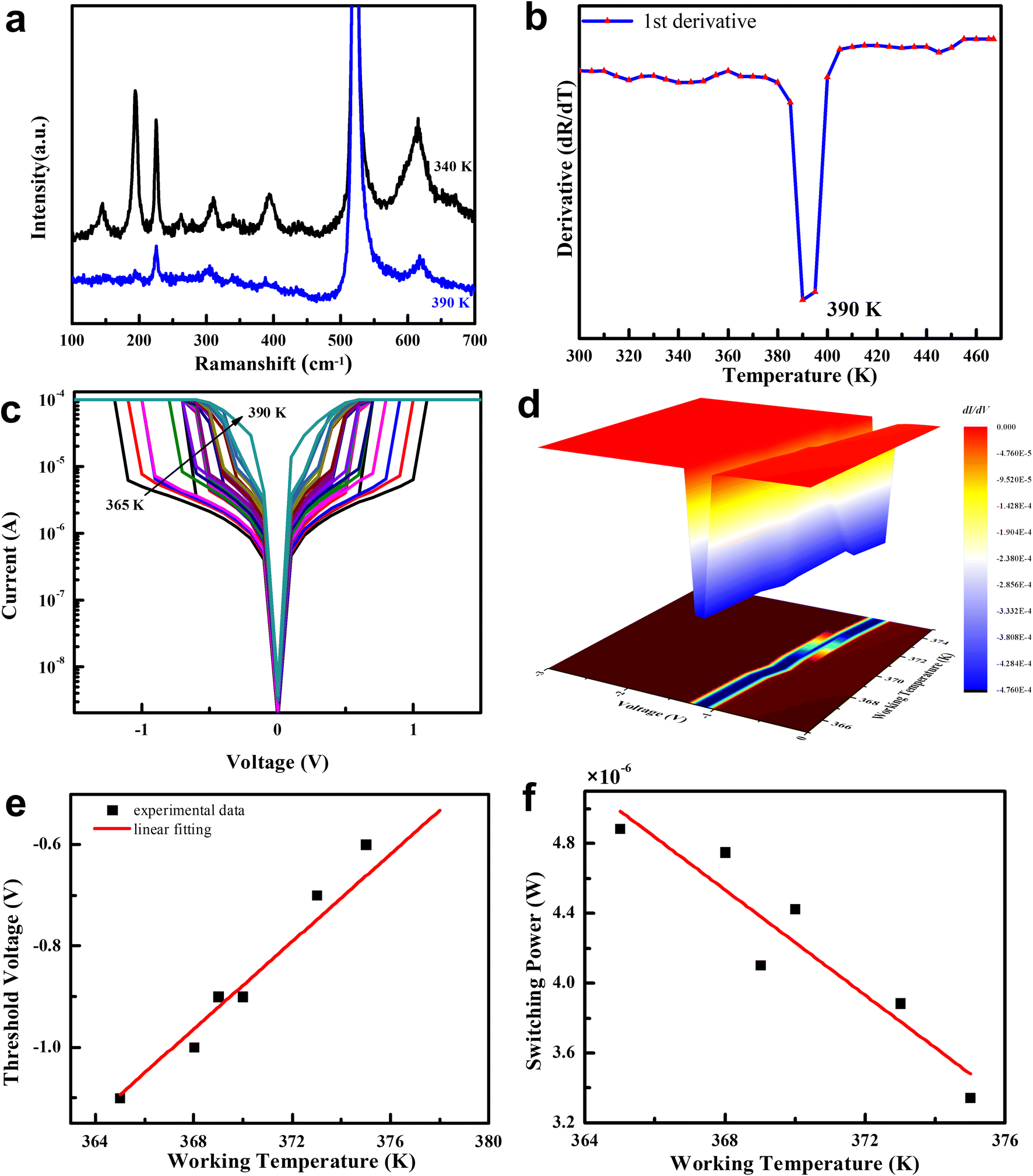 | ||
| Fig. 4 (a) Raman spectra of the VO2 nanowires deposited under different pressures. (b) Derivative resistance under variable temperatures of the two-terminal device based on VO2 nanowires with a transition point of 390 K. (c) I–V curves of the two-terminal device based on VO2 with a transition temperature of 390 K. (d) Map of differential conductance (dI/dV) as a function of the temperature and bias voltage. (e) Plots of threshold voltage and (f) switching power versus working temperature and the fitting curve (red solid lines). | ||
In Fig. 4d, the Map of differential conductance also suggested a linear function between the working temperature and bias voltage, which were similar with these illustrated in Fig. 3. The similar trend of the varied threshold indicated a stable reproducibility of the adaptive threshold voltages. Further analysis about the threshold voltage and switching power were displayed in Fig. 4e and f. A depressed switching power was from 4.8 μW to 4.2 μW. All these suggested the adaptive voltage and power scaling RS could be flexibly controlled and even programmed when we exploited the IMT processes in a widening range of operating temperature.
Furthermore, we analyzed the mechanism behind IMT-based energy-adaptive RS in briefly. It had been confirmed that the competition between coulomb repulsion energy and kinetic energy of the carrier determined the IMT process in strongly correlated system.54 When the magnitude of external perturbation and coulomb repulsion energy were basically consistent, the delocalized carrier corresponded to the high kinetic energy of the increased density of free electrons would turn the system to be metal state.55 In our case, the density of free electrons was directly related to field assisted carrier injection or increased working temperature. As to insulator region, the initial insulation state got quickly restored when bias voltage was removed. In the equilibrium state, the decreased thresholds corresponded to a stable resistance value of the same magnitude, that was, the energy used to excite the IMT got reduced. But for the transition region, coexisting insulating state and metallic state56 promoted the delocalization energy to the same order of magnitude with coulomb repulsion energy. Higher ground states of kinetic energy got maintained accompanied by nonlinear attenuated resistances. With the decreased bias voltages, switching power also shown a nonlinear trend, and the system recovered to the intermediate state faster with a shrink hysteresis window.
Conclusions
In summary, we have demonstrated energy-adaptive RS with adjustable thresholds by the IMT features in VO2 nanowires. The switching thresholds are electric-related and thermal-dependent while the IMT-based RS can also adapt to different thermal environments or temperature variations. The self-adjusted switching powers demonstrate a well performed energy-adaptive resistive switching. Ongoing investigations are carrying out for in-depth manipulating and understanding in VO2 based energy-efficient memory. We think that such thermal-adaptive switching helps reduce energy consumption, and shows promise in the construction of advanced Mott memory and correlated in-memory devices.Experimental section
Device fabrication
VO2 nanowires were deposited on silica/silicon substrates as we previously reported.51 Briefly, V2O5 powers were placed in the center of the quartz boat, and the clean substrate was placed downstream. The growth temperature was set at 900 °C, whereas the deposited time was about 20 minutes. UV lithography was then exploited to fabricate the device based on VO2 nanowires while the channel length was about 10 μm. Metal electrodes (Au/Cr, 100/20 nm) were deposited by the thermal evaporation.Device characterization
The morphology and microstructure of the grown VO2 nanowires were characterized by Optical microscope (Nikon Cis), scanning electron microscope (FEI Sirion200), Raman spectroscope (Nanofinder 30) (TII Tokyo Instruments, Inc.), X-ray diffraction (D/MAX2200), and X-ray photoelectron spectroscopy (Thermo ESCALAB 250Xi) were adopted for the measurements. Electrical behaviors were recorded on a cryogenic probe station (Lakeshore TTPX) with a semiconductor characterization system. Under DC condition, we swept the bias voltage with 0.1 V step based on Keithley 2636B and LabVIEW-based I–V test software and the starting voltage was 0 V.Conflicts of interest
There are no conflicts to declare.Acknowledgements
This work was funded by NSFC (92064014, 11933006), the National Key R&D Program of China, SCTSM (18J1414900) and Youth Innovation Promotion Association CAS.References
- B. Zhu, H. Wang, Y. Liu, D. Qi, Z. Liu, J. Yu, M. Sherburne, Z. Wang and X. Chen, Adv. Mater., 2016, 28, 1559–1566 CrossRef PubMed.
- S. Chen, Z. Lou, D. Chen and G. Shen, Adv. Mater., 2018, 30, 1705400 CrossRef PubMed.
- Z. Wei, K. Homma, K. Katayama, K. Kawai, S. Fujii, Y. Naitoh, H. Shima, H. Akinaga, S. Ito and S. Yoneda, IEEE Trans. Electron Devices, 2018, 65, 5189–5194 Search PubMed.
- C. Wu, T. W. Kim, J. H. Park, B. Koo, S. Sung, J. Shao, C. Zhang and Z. L. Wang, ACS Nano, 2020, 14, 1390–1398 CrossRef PubMed.
- N. Vasileiadis, V. Ntinas, G. C. Sirakoulis and P. Dimitrakis, Materials, 2021, 14, 5223 CrossRef CAS PubMed.
- C.-H. Huang, H. Chang, T.-Y. Yang, Y.-C. Wang, Y.-L. Chueh and K. Nomura, ACS Appl. Mater. Interfaces, 2021, 13, 52822–52832 CrossRef CAS.
- M. Mirigliano, D. Decastri, A. Pullia, D. Dellasega, A. Casu, A. Falqui and P. Milani, Nanotechnology, 2020, 31, 234001 CrossRef CAS.
- Y. van De Burgt, A. Melianas, S. T. Keene, G. Malliaras and A. Salleo, Nat. Electron., 2018, 1, 386–397 CrossRef.
- Z. Wang, W. Zhao, W. Kang, Y. Zhang, J.-O. Klein, D. Ravelosona and C. Chappert, Appl. Phys. Lett., 2014, 104, 104 Search PubMed.
- S. Yu, B. Gao, Z. Fang, H. Yu, J. Kang and H. S. P. Wong, Adv. Mater., 2013, 25, 1774–1779 CrossRef CAS.
- L. Tong, Z. Peng, R. Lin, Z. Li, Y. Wang, X. Huang, K.-H. Xue, H. Xu, F. Liu, H. Xia, P. Wang, M. Xu, W. Xiong, W. Hu, J. Xu, X. Zhang, L. Ye and X. Miao, Science, 2021, 373, 1353–1358 CrossRef CAS PubMed.
- M. D. Pickett, G. Medeiros-Ribeiro and R. S. Williams, Nat. Mater., 2013, 12, 114–117 CrossRef CAS.
- E. O. Neftci, Iscience, 2018, 5, 52–68 CrossRef.
- A. Sebastian, M. Le Gallo, R. Khaddam-Aljameh and E. Eleftheriou, Nat. Nanotechnol., 2020, 15, 529–544 CrossRef PubMed.
- I. Astrov, S. Tatarly and S. Tatarly, Adv. Electr. Comput. Eng., 2007, 7, 18–22 CrossRef.
- M. Aqib, R. Mehmood, A. Alzahrani, I. Katib, A. Albeshri and S. M. Altowaijri, Sensors, 2019, 19, 2206 CrossRef PubMed.
- K. S. Hale and K. M. Stanney, IEEE Comput. Graph., 2004, 24, 33–39 CrossRef PubMed.
- J. Pei, L. Deng, S. Song, M. Zhao, Y. Zhang, S. Wu, G. Wang, Z. Zou, Z. Wu, W. He, F. Chen, N. Deng, S. Wu, Y. Wang, Y. Wu, Z. Yang, C. Ma, G. Li, W. Han, H. Li, H. Wu, R. Zhao, Y. Xie and L. Shi, Nature, 2019, 572, 106–+ CrossRef CAS PubMed.
- C. Howarth, P. Gleeson and D. Attwell, J. Cereb. Blood Flow Metab., 2012, 32, 1222–1232 CrossRef CAS.
- C. Howarth, C. M. Peppiatt-Wildman and D. Attwell, J. Cereb. Blood Flow Metab., 2010, 30, 403–414 CrossRef.
- J. J. Yang, F. Miao, M. D. Pickett, D. A. A. Ohlberg, D. R. Stewart, C. N. Lau and R. S. Williams, Nanotechnology, 2009, 20, 215201 CrossRef.
- H. Fangohr, D. S. Chernyshenko, M. Franchin, T. Fischbacher and G. Meier, Phys. Rev. B: Condens. Matter Mater. Phys., 2011, 84, 054437 CrossRef.
- M. A. Leeves and F. McDonald, Am. J. Orthod., 1995, 107, 625–632 CrossRef CAS.
- N. Xu, J. Membr. Biol., 2013, 246, 75–90 CrossRef CAS.
- Y. Zhang, M. Khayatzadeh, K. Yang, M. Saligane, N. Pinckney, M. Alioto, D. Blaauw and D. Sylvester, IEEE J. Solid-State Circuits, 2018, 53, 619–631 Search PubMed.
- H. Fuketa, M. Hashimoto, Y. Mitsuyama and T. Onoye, IEEE T. VLSI Syst., 2012, 20, 333–343 Search PubMed.
- H. Reyserhove and W. Dehaene, IEEE J. Solid-State Circuits, 2018, 53, 2101–2113 Search PubMed.
- X. Hou, C. Liu, Y. Ding, L. Liu, S. Wang and P. Zhou, Adv. Sci., 2020, 7, 2002072 CrossRef PubMed.
- A. Mraz, R. Venturini, D. Svetin, V. Sever, I. A. Mihailovic, I. Vaskivskyi, B. Ambrozic, G. Drazic, M. D'Antuono, D. Stornaiuolo, F. Tafuri, D. Kazazis, J. Ravnik, Y. Ekinci and D. Mihailovic, Nano Lett., 2022, 22, 4814–4821 CrossRef.
- D. M. Blitz, J. Neurophysiol., 2017, 118, 949–963 CrossRef.
- D. M. Blitz and M. P. Nusbaum, J. Neurophysiol., 2012, 32, 9182–9193 Search PubMed.
- C. Y. L. Huh, J. P. Peach, C. Bennett, R. M. Vega and S. Hestrin, Curr. Biol., 2018, 28, 114–120 CrossRef PubMed.
- F. J. Morin, Phys. Rev. Lett., 1959, 3, 34–36 CrossRef.
- S. H. Chang, S. B. Lee, D. Y. Jeon, S. J. Park, G. T. Kim, S. M. Yang, S. C. Chae, H. K. Yoo, B. S. Kang, M. J. Lee and T. W. Noh, Adv. Mater., 2011, 23, 4063–4067 CrossRef PubMed.
- R. F. Janninck and D. H. Whitmore, J. Phys. Chem. Solids, 1966, 27, 1183–1187 CrossRef.
- S. Kim, J. Park, J. Woo, C. Cho, W. Lee, J. Shin, G. Choi, S. Park, D. Lee, B. H. Lee and H. Hwang, Microelectron. Eng., 2013, 107, 33–36 CrossRef.
- J.-Y. Lee, Y.-J. Baek, Q. Hu, Y. J. Choi, C. J. Kang, H. H. Lee, H.-M. Kim, K.-B. Kim and T.-S. Yoon, Appl. Phys. Lett., 2013, 102, 122111 CrossRef.
- X. Cao, Y. Han, J. Zhou, W. Zuo, X. Gao, L. Han, X. Pang, L. Zhang, Y. Liu and S. Cao, ACS Appl. Mater. Interfaces, 2019, 11, 35914–35923 CrossRef CAS.
- Z. Li, Y. Guo, Z. Hu, J. Su, J. Zhao, J. Wu, J. Wu, Y. Zhao, C. Wu and Y. Xie, Angew. Chem., Int. Ed., 2016, 55, 8018–8022 CrossRef CAS PubMed.
- M. Nakano, K. Shibuya, D. Okuyama, T. Hatano, S. Ono, M. Kawasaki, Y. Iwasa and Y. Tokura, Nature, 2012, 487, 459–462 CrossRef CAS.
- M. Liu, H. Y. Hwang, H. Tao, A. C. Strikwerda, K. Fan, G. R. Keiser, A. J. Sternbach, K. G. West, S. Kittiwatanakul, J. Lu, S. A. Wolf, F. G. Omenetto, X. Zhang, K. A. Nelson and R. D. Averitt, Nature, 2012, 487, 345–348 CrossRef CAS.
- J. Cao, E. Ertekin, V. Srinivasan, W. Fan, S. Huang, H. Zheng, J. W. L. Yim, D. R. Khanal, D. F. Ogletree, J. C. Grossmanan and J. Wu, Nat. Nanotechnol., 2009, 4, 732–737 CrossRef CAS PubMed.
- J. Jian, X. Wang, L. Li, M. Fan, W. Zhang, J. Huang, Z. Qi and H. Wang, ACS Appl. Mater. Interfaces, 2017, 9, 5319–5327 CrossRef CAS PubMed.
- S. Wang, W. Wei, T. Huang, T. Zhang, Z. Chen, L. Sun, H. Xia, T. Li, X. Chen, X. Chen, W. Lu and N. Dai, Adv. Mater. Interfaces, 2018, 5, 1800374 Search PubMed.
- J. H. Parker, D. W. Feldman and M. Ashkin, Phys. Rev., 1967, 155, 712–714 CrossRef CAS.
- Y. Kalcheim, A. Camjayi, J. Del Valle, P. Salev, M. Rozenberg and I. K. Schuller, Nat. Commun., 2020, 11, 2985 CrossRef CAS PubMed.
- D. Bersani, P. P. Lottici and A. Montenero, J. Raman Spectrosc., 1999, 30, 355–360 CrossRef CAS.
- T. Huang, S. Wang, W. Wei, Y. Yang, W. Yang, M. Yuan, R. Zhang, T. Zhang, X. Chen, Y. Sun, X. Zhou, J. Shao, X. Chen and N. Dai, Phys. Status Solidi B, 2020, 257, 1900785 CrossRef CAS.
- J. Mendialdua, R. Casanova and Y. Barbaux, J. Electron Spectrosc. Relat. Phenom., 1995, 71, 249–261 CrossRef CAS.
- G. Silversmit, D. Depla, H. Poelman, G. B. Marin and R. De Gryse, J. Electron Spectrosc. Relat. Phenom., 2004, 135, 167–175 CrossRef CAS.
- W. Wei, T. Huang, S. Wang, W. Luo, T. Zhang, W. Hu, X. Chen and N. Dai, Phys. Status Solidi RRL, 2019, 13, 1900383 CrossRef CAS.
- S. Wang, W. Wei, T. Huang, T. Zhang, Z. Chen, X. Chen and N. Dai, Adv. Eng. Mater., 2019, 21, 1900947 CrossRef CAS.
- J. Wei, Z. Wang, W. Chen and D. H. Cobden, Nat. Nanotechnol., 2009, 4, 420–424 CrossRef CAS.
- N. F. Mott, Phys. Soc. A, 1949, 62, 416–422 CrossRef.
- Y. Zhou and S. Ramanathan, Proc. IEEE, 2015, 103, 1289–1310 CAS.
- M. M. Qazilbash, M. Brehm, B.-G. Chae, P. C. Ho, G. O. Andreev, B.-J. Kim, S. J. Yun, A. V. Balatsky, M. B. Maple, F. Keilmann, H.-T. Kim and D. N. Basov, Science, 2007, 318, 1750–1753 CrossRef CAS.
Footnotes |
| † Electronic supplementary information (ESI) available. See DOI: https://doi.org/10.1039/d2ra06866d |
| ‡ T. Huang and R. Zhang contributed equally to this work. |
| This journal is © The Royal Society of Chemistry 2022 |