DOI:
10.1039/D2RA06581A
(Paper)
RSC Adv., 2022,
12, 33988-34005
Topological defects and nanoholes in graphene oxide/hexagonal boron nitride heterostructures: stress buildup and accumulation
Received
18th October 2022
, Accepted 22nd November 2022
First published on 29th November 2022
Abstract
The built-in distorted stress field of graphene (Gr) and its derivatives in defective state will induce local geometrical buckling due to the geometry of monatomic layer. The random distribution and types of functional groups (FGOs) and defects will have a significant impact on the stress accumulation and geometrical deformation of two-dimensional (2D) materials. By using molecular dynamics (MD), structure design and nonlinear mechanics theory, a new model (combining both planar 2D heterostructures and graphene oxide (GO)) was established to study geometrical effects, stress accumulation, bonding energies and mechanical properties of 2D interface (key point) at stress distortion field and accumulated stress field. The results show that grain boundaries (GBs), nanoholes and FGOs have different effects on the mechanical properties and out-of-plane deformation of 2D materials. By using Von-mises stresses and statistical mechanics, the geometrical effects, built-in distortion stress transfer and attenuation appeared in the each domain of 2D materials during the order–disorder transition processes. Moreover, there are two opposite aspects of stress accumulation, transmission, attenuation and geometrical effects of grain boundary (GBs), FGOs and nanoholes with distance. The ratio of strain energy (bond length and angle) is very sensitive to each domain of 2D materials. Finally, the 2D planar configuration gradually changes to a negative Gaussian surface, and the softening and weakening effects induced by GBs, nanoholes and FGOs are gradually enhanced. It is hoped that the current results can be used as a guide to adjust the geometry and stress accumulation of 2D materials in the new growth point.
1 Introduction
The geometric effect in 2D materials is a fundamental problem that cannot be avoided in the mechanical characterization of 2D materials. As a 2D material of monatomic layer, Gr has low bending rigidities, but its bending stiffness is not zero.1 The Gr is similar to the bending rigidities of cell membrane, about 1 eV.2 For a large scale of defect-free Gr, the folded morphology is usually only formed at its edge.3 Gr nanosheets can also form curled shapes due to van der Waals force adsorption between parts.2 Therefore, Gr film is prone to large-scale thermal fluctuation displacement and deformation due to external disturbance in the equilibrium state.4
The geometrical morphology of Gr depends not only on the thermal disturbance of external environment and its own geometrical size, but also on its internal defect structure.5 The existence of GBs and nanoholes will not only generate built-in distortion stress in 2D materials, but also cause buckling deformation of structures, especially in 2D materials with low bending stiffness such as Gr.6,7 Z. G. Song et al.8 used the combination and superposition of basic defect structures and stress fields to explore the stress field distribution of common defects in Gr. Their result indicated that the pseudo (inverse) Hall–Petch effect is found in the brittle fracture behavior of polycrystalline Gr, that is, the tensile strength is inversely related (positively related) to the grain size. In addition, triple GBs junctions serve as the nucleate centers for cracks and crack propagation. In another work, the effect of topological defects on geometrical deformation of Gr was investigated. The result shows that a single 5|7 dislocation in 2D hexagonal lattice will induce it to deviate from the plane configuration, and produce cone and saddle shapes with positive and negative curvature, respectively.5 J. Xu et al. also proved9 that the structural engineering of graphene and even other 2D materials will broaden the photoelectric application. In another work, Y. T. Niu et al.10 confirmed that the inhomogeneous spatial distribution of strain and doping can control the physical properties of graphene.
Compared with three-dimensional bulk materials, defects such as vacancy, doping and dislocation have more significant effects on the physical properties of 2D materials.11–13 These defects can significantly change the overall properties of Gr derivative and heterostructures. The rigidity and strength characteristics of Gr derivative and heterostructures were weakened. Then, the scattering of electron and phonon transport was also affected.14–17 More importantly, this kind of built-in distortion stress can lead to the secondary mechanical behaviors of 2D materials, such as sliding, buckling, folding, breaking and out-of-plane movement of 2D materials. It is directly coupled with the growth reaction, and then changed the growth process of materials.
GO is a non-stoichiometric material with layered structure, with hydroxyl (–OH) and epoxy groups (–O) on the surface and carboxyl (–COOH) on the edge.18,19 These functional groups (FGOs) provide a large number of active sites for connecting various organic small molecules, polymers, biological macromolecules and other FGOs.20,21 Due to the uneven distribution of oxygen-containing groups in GO, the sp2 hybrid region is separated into “islands” with a size of 2–3 nm by the sp3 hybrid C–O.22,23 Moreover, a large number of folds are produced on the surface of GO due to the distortion of sp3 hybridization to form tetrahedral structure. After calculation, the bending rigidities of Gr derivative are also similar to cell membrane.24 It is worthy notice that Gr derivative is very easy to bend and fold. Although reduced GO is similar to Gr nanostructure and has similar properties (good conductivity, etc.), RGO usually contains more defects and is lower in quality than Gr directly produced from graphite. Moreover, reduced GO contains residual oxygen and other heteroatoms.
Will the coupling of these internal fields coupling (GBs, FGOs and nanoholes) lead to local buckling of 2D materials? Whether the internal field coupling effect increases, decreases or remains the same for mechanical properties of 2D materials? From the perspective of structural design, stress accumulation and energy, combining both planar 2D heterostructures and GO opens up the possibility to create an unprecedented architecture using 2D atomic layer.
The fracture characteristics, geometric deformation and bond energies induced by GBs and nanoholes in GO configurations were investigated. The topological and geometrical effects of the coupling effects of GBs and nanoholes on the distribution and types of FGo as well as spatial configuration of GO nanostructures were analyzed. By using GBs and nanopore to control the geometry of 2D materials, nano-structures such as nano-cones and hourglass channels can be constructed. It can be used in the design of functional devices such as transmission channels.
2 Computational model and method
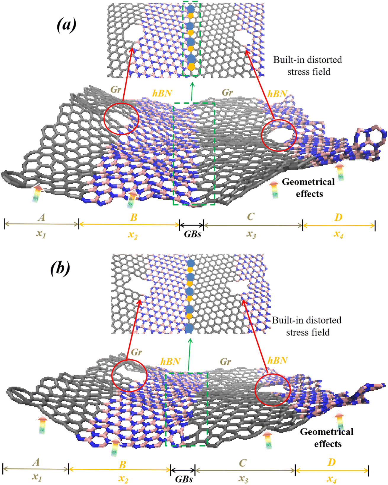
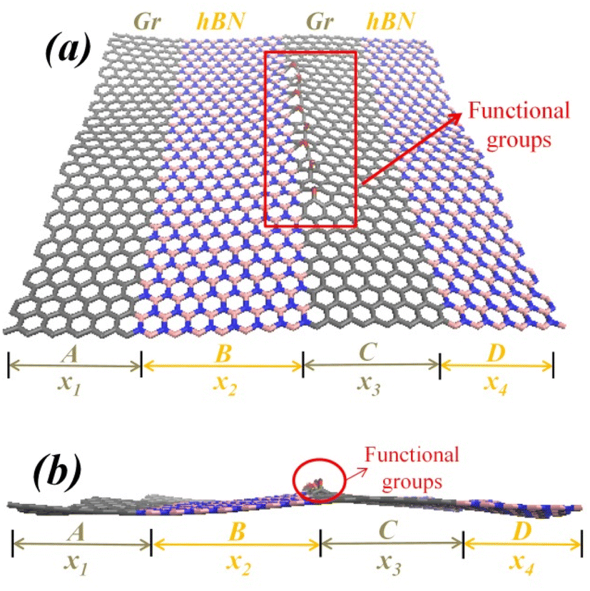
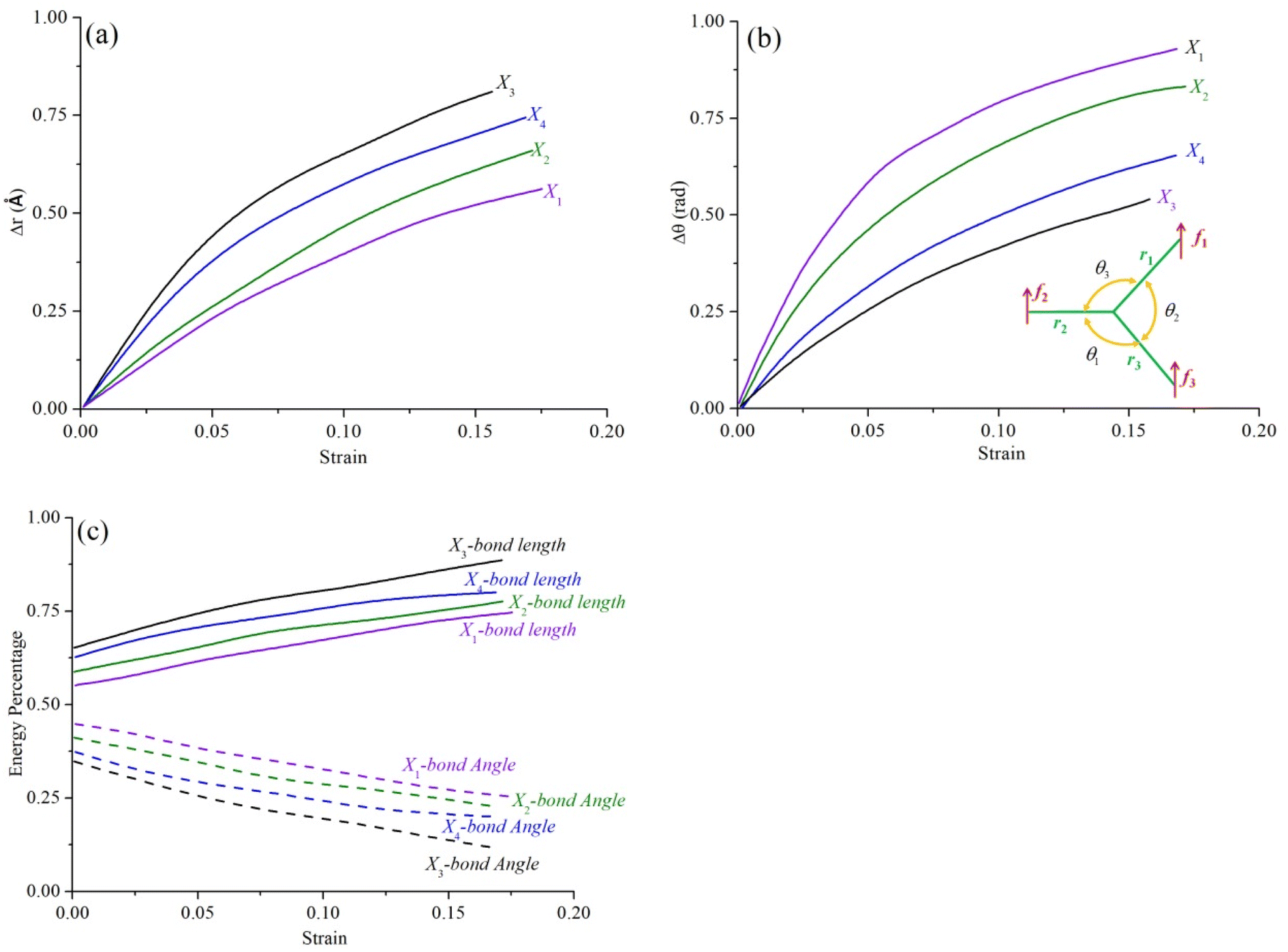
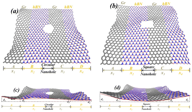
The formation process of Gr–hBN heterostructures with GBs can be seen as the overlapping of a perfect Gr and a perfect h-BN after rotating at a certain angle. When the atoms in the overlapping region cannot be arranged according to the six-ring structure of perfect Gr. The GBs is formed at the in-plane structures. Next, it is assumed that Gr and hBN are two parts of region (B) and region (C), respectively. An hBN layer (region (B)) has been butt-joined to the left sides of a Gr layer region (C), and then creating GBs in their interface. Moreover, by using structure design theory, another layer of Gr (region (A)) has been butt-joined to the left sides an hBN layer (region (B)), and another layer of an hBN (region (D)) has been butt-joined to the left sides of a Gr layer (region (D)). A new graphene–hBN–graphene–hBN (Gr–BN interface) configuration was constructed by creating nanoholes and GBs in their interface, including a nanoholes (at interface between A and B regions), GBs (at interface between B and C regions), a nanoholes (at interface between C and D regions). A hybrid Gr–BN interface with nanoholes and GBs at the interface of their layers was shown in Fig. 1.
 |
| | Fig. 1 A hybrid Gr–BN with nanoholes and GBs at the interface of their layers. (a) Geometrical effects induced by circular nanoholes and GBs and (b) geometrical effects induced by square nanoholes and GBs. | |
The GBs of Gr–BN interface nanostructures can be defined by using mismatch angle (θ):
| |
 | (1) |
where
θR and
θL are the rotation angles of the left and right parts, respectively.
Any non-six ring structure in the GBs is considered as a defect. If the defects are arranged periodically, the GBs can be characterized by the period length (Lp) of adjacent defects. The periodic length (Lp) can be expressed by the translation vector pairs (nL, mL)|(nR, mR) on both sides of the GBs:
| |
 | (2) |
| |
 | (3) |
where
α0 is the unit vector of h-BN lattice, and
β0 is the unit vector of Gr lattice.
n and
mis the translation vector of system.
nR and
mR is the translation vector of h-BN, and
nL and
mL is the translation vector of Gr.
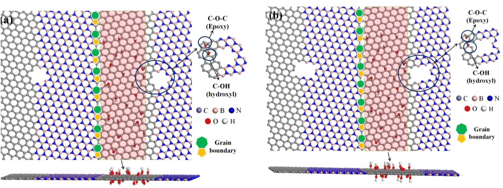
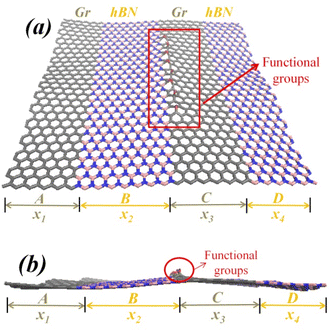
In order to deeply study the topological and geometric effects of the coupling effects of GBs and nanoholes on the distribution and types of different FGOs as well as the spatial configuration of GO nanostructures. A series of FGOs (epoxy (C–O–C), hydroxyl (C–OH) and their combination (C–O–C + C–OH) are created in defective Gr–BN interface nanostructures, as shown in Fig. 2(a–b).
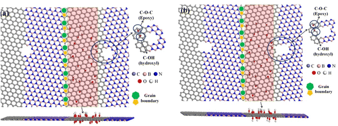 |
| | Fig. 2 A defective Gr–BN interface nanostructures with FGOs at the B–C region. (a) Gr–BN interface nanostructures with circular nanoholes, GBs and FGOs (GO–BN–C) and (b) Gr–BN interface nanostructures with square nanoholes, GBs and FGOs (GO–BN–S). | |
It is noted that the density of FGOs in Gr–BN interface nanostructures can be defined as R.
| |
 | (4) |
where
Nc is the total number of carbon atoms in Gr–BN interface with FGOs nanostructures, and
Nη is the number of carbon atoms connected to the FGOs.
The whole working case is realized by using large-scale atomic/molecular massively parallel simulator (LAMMPS).25
Tersoff potential is suitable for describing the short-range interaction of nitrogen (N), boron (B) and carbon (C) atoms.26,27 ReaxFF is employed to describe the bond dynamics and interatomic interactions between hydrogen (H), oxygen (O) and C atoms, as well as the parameters proposed by V. Akarsh et al.28 Also, the interactions between N and O are characterized by charge-optimized COMB potential, which has been studied by T. Liang, et al.29 The interactions between B and O were characterized parametrically by Teter, which was investigated by L. Deng.30 The hydrogen–nitrogen and hydrogen–boron bonds are very high, and the reaction self-consistent force field can only be used to accurately simulate.31
The simulation for Gr–BN interface with FGOs nanostructures can be divided into two stages. In the relaxation stage, the spatial configuration was first equilibrated using an NPT system with Nosé–Hoover method to control pressure and temperature, at a time step of 0.5 fs. The entire penetration process is simulated and calculated for 500 ps under the condition of NPT ensemble at 300 K temperature and 1 atm pressure. After this relaxation stage, the system is converted to NVT ensemble at 300 K, running for 200 ps. Finally, this simulation model runs at 300 K for another 500 ps to generate atomic trajectory information for data analysis. The strain rate of the GO-BN-GBs configuration is assumed to 0.001 ps−1.
The Young's modulus E was calculated as the initial slope of the stress–strain curves, and the failure strength σ was taken as the peak stress of the curves.
To obtain the stress–strain curves during deformation, the atomic stress of individual atoms in the Gr–BN interface with FGOs nanostructures were calculated according to the following eqn (5):32
| |
 | (5) |
where
ς and
ψ denote the indices in the Cartesian systems;
α and
β are the atomic indices;
mα and
vα denote the mass and velocity of the atom α, respectively;
rαβ is the distance between the atoms α and β; and
Ωα is the atomic volume of the atom α. After obtaining the stress of each atom, the stress of the Gr–BN interface with FGOs nanostructures were computed by averaging over all the atoms in the nanostructures. The failure strength was taken as the peak stress of the stress–strain curves. Similarly, the failure strain was taken as the peak strain of the stress–strain curves. It is worth mentioning that both sides of hybrid nanostructures contain functional groups. If only one side (upper surface or lower surface) contains functional groups, the geometric deformation and deflection of heterojunction will change greatly due to the asymmetric effect.
3 Results and discussion
3.1 Validation
To verify the simulation, Table 1 show the results of previous work compared with the three mechanical values (fracture stress, strain, and Young's modulus) of Gr and hBN in this study. As shown in Table 1, the comparison shows that the calculation method and the selection of potential function were very reasonable, and the results obtained were very consistent with previous work. The Young's modulus of the pristine Gr was 921 GPa. In addition, the Young's modulus of the pristine hBN was 915 GPa. The simulated results were in good agreement with the experimental result (1000 GPa for Gr34 and 881 GPa for hBN36), the DFT result (1050 GPa for Gr33 and 863 GPa for hBN35) and MD result (930 GPa for Gr26 and 930 GPa for hBN26).
Table 1 Comparing the Young's modulus, failure strength, and strain values of pure graphene and hBN obtained by the present study and by previous experimental and computational works
| Various types |
Assessment method (potential) |
Failure strain |
Failure strength (GPa) |
Young's modulus (GPa) |
Ref. |
| Single-layer |
MD (Tersoff) |
0.203 |
124 |
921 |
Present study |
| Single-layer |
MD (Tersoff) |
0.201 |
131 |
930 |
Eshkalak et al.26 |
| Single-layer |
DFT |
0.208 |
127 |
1050 |
Liu et al.33 |
| |
Experimental |
0.25 |
130 |
1000 |
Lee et al.34 |
| Single-layer |
MD (Tersoff) |
0.199 |
121 |
915 |
Present study |
| Single-layer |
MD (Tersoff) |
0.2 |
131 |
930 |
Eshkalak et al.26 |
| Single-layer |
DFT |
0.19 |
120 |
863 |
Ding et al.35 |
| |
Experimental |
— |
— |
881 |
Bosak et al.36 |
3.2 Effect of GBs on mechanical properties
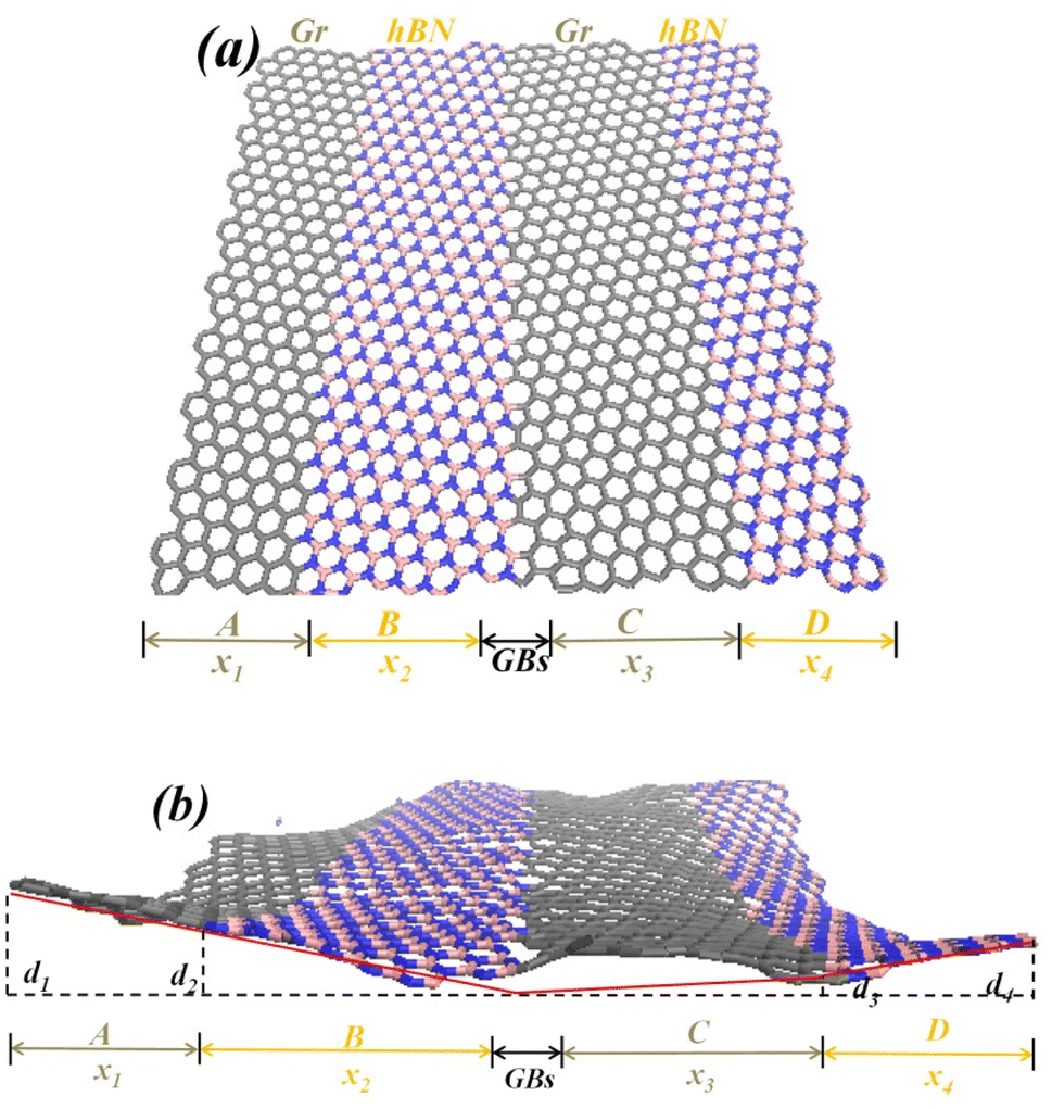
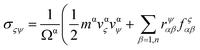
The coupling of defects has significant effects on the mechanical properties, crystalline structure and structural deformation of 2D materials. These influences are not simply 1 + 1 = 2, while it is a complex distortion effect for stress, strain and structural deformation (it may be a superposition positive effect or a superposition negative effect). The effect of single internal field (GBs) on the out-of-plane displacement of Gr–BN interface was investigated. Fig. 3 shows the out-of-plane displacement of Gr–BN interface with GBs. It is found from Fig. 3 that the existence of GBs cause 3D out-of-plane displacement of the 2D structure. A series of out-of-plane displacement (d1, d2, d3 and d4) were formed in key regions of Gr–BN interface with GBs, including Gr edge, hBN edge and their interfaces (see Fig. 3(b)). In addition, the out-of-plane displacement values are different in each region of Gr–BN interface with GBs. The highest value of out-of-plane displacement are found at Gr edge (A region) of Gr–BN interface with GBs, while the lowest value of out-of-plane displacement are obtained at center region (GBs) of Gr–BN interface with GBs. At the center interface regions (GBs), the spatial structure of Gr–BN interface with GBs is relatively low position, compared with other regions. It is noticed that the spatial structure of Gr–BN interface with GBs is a 3D concave shape, instead of a planar 2D structure.
 |
| | Fig. 3 The geometrical deformation of Gr–BN interface with different Lp of GBs. (a) Plane view of a portion of Gr–BN interface with GBs and (b) a perspective side-view of a portion of Gr–BN interface with GBs. | |
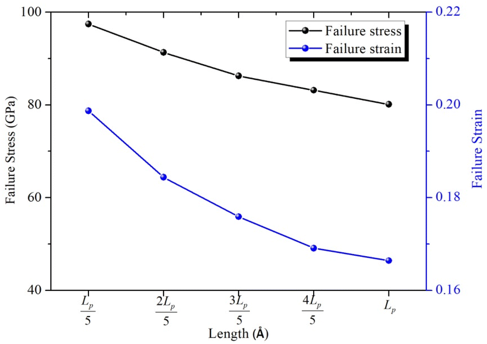
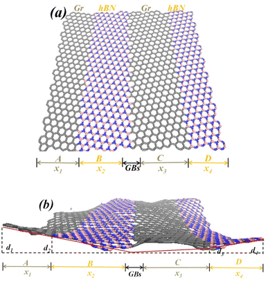
We turn our attention to the effect of GBs on the mechanical properties of Gr–BN interface with GBs nanostructures. Considering the different Lp of GBs, the failure stress and strain of Gr–BN interface with GBs were studied, as shown in Fig. 4. It is found that the failure stress and strain of Gr–BN interface with GBs increase with increase of Lp of GBs. Because the GBs promotes the out-of-plane displacement of 2D materials, and out-of-plane displacement has a greater impact on local mechanical response of 2D materials. During the process of tension, the out-of-plane displacement and deformation of Gr–BN interface with GBs are an uneven distribution, and the degree of uneven distribution is closely to Lp of GBs. More importantly, C–C, B–N, C–B and C–N bonds near GBs will bear greater stress, relative to Gr–BN interface with no GBs.
 |
| | Fig. 4 The mechanical properties of Gr–BN interface with different Lp of GBs. | |
3.3 Effect of defects on mechanical properties
The previous studies37–39 have confirmed that the defects decreased the mechanical properties of 2D materials, and the reduction degree of mechanical properties is closely to defect types and defect numbers. However, the above-mentioned calculation and simulation studies on the fracture behavior of 2D materials are mostly based on the planar 2D model, but the real 2D materials usually contains out-of-plane displacement under the external and internal field. Therefore, the out-of-plane displacement and mechanical properties of Gr–BN interface with nanoholes (circular and square) were investigated, as shown in Fig. 5 and 6. It is found from Fig. 5 that the existence of defects has important effects on the out-of-plane displacement of Gr–BN interface with nanoholes. However, the effect of defects and GBs on the out-of-plane displacement is different. The out-of-plane displacements are formed in Gr–BN interface with nanoholes due to the loss of atoms. The more these atoms are eliminated and thus, the more the forces balances between atoms are damaged and broken up, the higher out-of-plane displacements will be. In view of the resulting out-of-plane displacements, the existence of square nanoholes in Gr–BN interface leads to greater out-of-plane displacements than the presence of circular nanoholes (see Fig. 5(c) and (d)). Obviously, the d1 and d4 at edge region are higher than d2 and d3 at interface region (without defects) and at central interface region (square nanoholes).
 |
| | Fig. 5 The out-of-of displacement of Gr–BN interface with different nanoholes. (a) Plane view of a portion of Gr–BN interface with circular nanoholes, (b) plane view of a portion of Gr–BN interface with square nanoholes, (c) perspective side-view of a portion of Gr–BN interface with circular nanoholes and (d) perspective side-view of a portion of Gr–BN interface with square nanoholes. | |
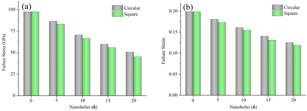 |
| | Fig. 6 The mechanical properties of Gr–BN interface with different nanoholes. (a) Failure stress and (b) failure strain. | |
It is observed from Fig. 6 that the existence of square nanoholes in Gr–BN interface leads to a more reduction values of failure stress and strain than the existence of circular nanoholes. The reason is that square nanoholes leads to a more reduction of atoms from Gr–BN interface and also the elimination of more hexagonal rings in their interface. Obviously, the failure stress and strain of Gr–BN interface with circular nanoholes is higher than that of Gr–BN interface with square nanoholes. In addition, the failure stress and strain values do follow a regular and similar trend. The failure stress and strain values decrease with increase of nanoholes sizes.
3.4 Effect of FGOs on mechanical properties
The effect of FGOs on out-of-plane displacement and mechanical properties of Gr–BN interface was studied, as shown in Fig. 7 and 8. It is observed from Fig. 6 that out-of-plane displacement of Gr–BN interface with different FGOs does follow a similar trend, relative to above two simulations. Although GBs, defects or FGOs are generated in the same region, the out-of-plane deformation of 2D structures caused by defects, GBs and FGOs are different. The vacancy defects cause changes in the number of atoms and 6-rings. The GBs keeps the number of atoms and 6-rings unchanged, while the 6-rings are transformed into 5–7 rings. Also, the sp2 hybrid structures have changed to hybrid state of sp3 bonding by introducing the FGOs. Obviously, the spatial configuration of Gr–BN interface with FGOs is a cone shape (see Fig. 7(b)), and the apex of the cone shape is located at FGOs area (interface region). Obviously, the out-of-plane displacement at central interface region is higher than that of other regions.
 |
| | Fig. 7 The geometrical deformation of Gr–BN interface with different FGOs nanostructures. (a) Plane view of a portion of Gr–BN interface with different FGOs and (b) perspective side-view of a portion of Gr–BN interface with different FGOs. | |
 |
| | Fig. 8 The mechanical properties of Gr–BN interface with different FGOs. (a) Failure stress and (b) failure strain. | |
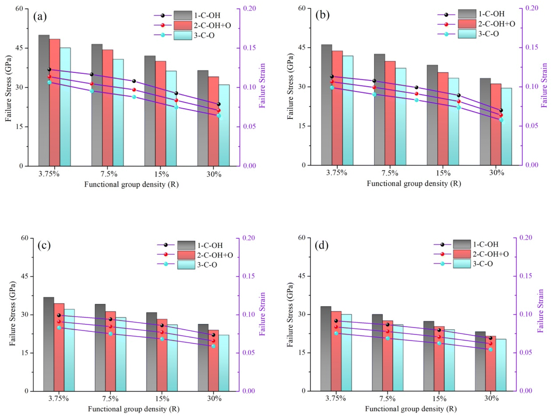
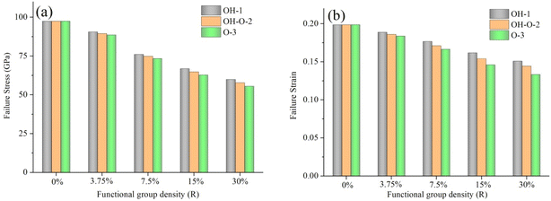
Next, we turn our attention to the effect of FGOs on failure stress and strain of Gr–BN interface. The Gr–BN interface with FGOs nanostructures were divided into 3 parts: OH-1 (only hydroxyl groups), OH–O-2 (hydroxyl + epoxy groups) and O-3 (epoxy groups). Fig. 8 shows the failure stress and strain of Gr–BN interface with different FGOs. It is found from Fig. 8 that failure strain of OH-1 varies from 0.1987 to 0.1618 when the densities of OH-1 are increased from 0% to 15%. The Gr–BN interface with FGOs nanostructures possesses lower mechanical properties than the pristine one, and the percentage of difference is closely to the densities and types of FGOs. Clearly, the presence of FGOs has an adverse effect on the failure stress and strain of Gr–BN interface with FGOs nanostructures.
In considering the same densities of FGOs, the highest failure stress and strain values are achieved when OH-1 are created at central interfaces. Nevertheless, the lowest failure stress and strain values are obtained when O-3 are created at central interfaces.
A key conclusion is that the internal field (defects, GBs and FGOs) affect the mechanical properties of Gr–BN interface nanostructures in two contrary ways. On one hand, the presence of internal field can lead to a reduction in the failure stress and strain. On the other hand, the presence of internal field changes spatial configuration and out-of-plane displacement. The flattening of out-of-plane displacement can significantly reduce the tensile ratio of covalent bonds, resulting in a significant increase of failure strain.
3.5 Internal effects (GBs, nanoholes and FGOs) for geometrical deformation
Fig. 9 shows the fracture strength and strain of defective Gr–BN interface nanostructures in different cases, including nanoholes shape (circular and square), nanoholes sizes (10 Å and 20 Å), FGOs types (C–OH, C–O–C and C–OH + C–O–C) and FGOs density. According to Fig. 9, the fracture strength and strain are reduced by increasing the nanoholes sizes and the FGOs density in the of defective Gr–BN interface nanostructures. In the interface zone, by increasing the dimensions of circular nanoholes from 10 to 20 Å, the fracture strength and strain of 2-C–OH + O model are reduced by 21.89% and 12.96%, respectively. While the fracture strength and strain are reduced by 11.31% and 6.17% for the 10 Å square nanoholes, compared with 10 Å circular nanoholes. The GO–BN-C1 generally has better fracture strength and strain than those with GO–BN-S1 (square nanoholes) due to more bonding failure and stress accumulation.
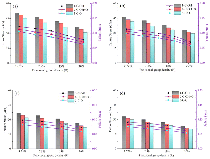 |
| | Fig. 9 The fracture strength and strain of Gr–BN interface nanostructures in different cases. (a) Gr–BN interface with 10 Å circular nanohole, GBs and FGOs (GO–BN–C1), (b) Gr–BN interface with 10 Å square nanohole, GBs and FGOs (GO–BN–S1), (c) Gr–BN interface with 20 Å circular nanohole, GBs and FGOs (GO–BN–C2) and (d) Gr–BN interface with 20 Å square nanohole, GBs and FGOs (GO–BN–S2). The 1-C–OH, 2-C–OH + O and 3-C–O represent the Gr–BN interface with C–OH, C–O–C and C–OH + C–O–C, respectively. | |
In this respect, in the x3 region (with circular nanoholes), the best fracture strength and strain are obtained when the C–OH are created at accumulated stress field. However, the worst fracture strength and strain are obtained when the C–O–C are created at accumulated stress field. Also, in the case in which the nanoholes and FGOs are displaced to in the same regions, the fracture strength and strain do follow a similar trend. It is evident that FGOs types have a greater influence on the fracture strength and strain of defective Gr–BN interface nanostructures. In the x3 region, by changing the types of FGOs from 1-C–OH to 2-C–OH + O, the fracture strength and strain are reduced by 8.81% and 16.13%, respectively. When compared with the 1-C–OH, the presence of the 3-C–O results in 10.46% and 19.70% reduction in the fracture strength and strain. For the three cases which the types of FGOs vary in the x3 region, the changes of fracture strength and strain do not follow a regular trend. It is expected that the degree of reduction will increase with increasing FGOs density. With regard to the fracture strain at which the fracture strength is investigated, it is confirmed that defective Gr–BN interface nanostructures undergoes fracture at the strain level varying from 0.0958 to 0.0644 when the fraction of FGOs (3-C–O) increases from 3.75% to 30%. Likewise, the existence of FGOs plays an opposite role in the fracture strength and strain of defective Gr–BN interface nanostructures (locations between GBs and nanoholes).
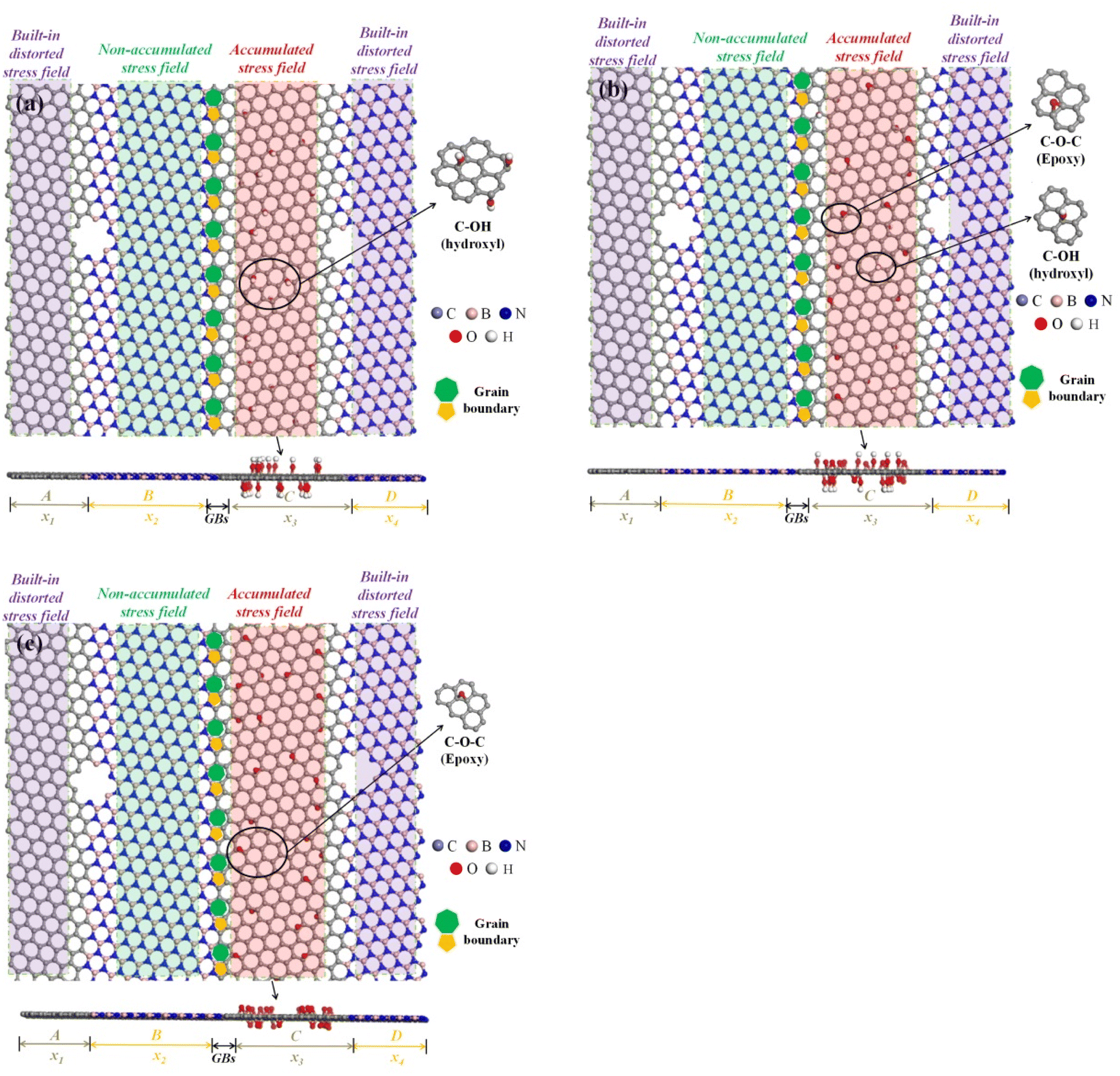
In order to explore the effects of FGOs distribution and types on the stress accumulation and geometrical effects of defective Gr–BN interface nanostructures (key weaknesses region), and the accumulated stress field (red region, FGOs are between nanoholes and GBs), the non-accumulated stress field (green region, FGOs are not between nanoholes and GBs) and the built-in distorted stress field (purple region) are considered, as shown in Fig. 10.
 |
| | Fig. 10 The perspective and plane view of a portion of a Gr–BN with FGOs nanostructures in different cases. (a) Gr–BN interface with hydroxyl groups (C–OH), (b) Gr–BN interface with hydroxyl and epoxy groups (C–OH + C–O–C) and (c) Gr–BN interface with epoxy groups (C–O–C). | |
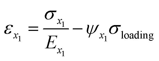
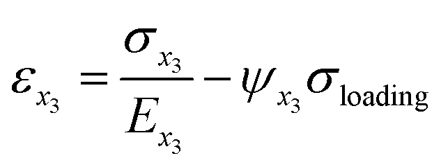
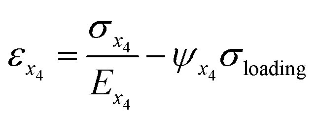
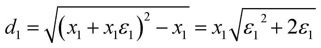
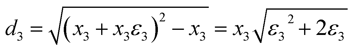
The fracture strength and strain in defective Gr–BN interface nanostructures are divided into A(x1) domain, B(x2) domain, C(x3) domain and D(x4) domain. The geometrical deformation induced by GBs, nanoholes and FGOs in four domains of defective Gr–BN interface nanostructures can be calculated by the following eqn (6)–(13):40
| |
 | (6) |
| |
 | (7) |
| |
 | (8) |
| |
 | (9) |
| |
 | (10) |
| |
 | (11) |
| |
 | (12) |
| |
 | (13) |
where
εx1,
εx2,
εx3 and
εx4 are the strain of
x1,
x2,
x3 and
x4 domain, respectively.
σx1,
σx2,
σx3 and
σx4 are the stresses of
x1,
x2,
x3 and
x4 domain, respectively.
σloading is the tension loading.
ψx1,
ψx1,
ψx1 and
ψx1 are the Passion ratios of corresponding domains.
Ex1,
Ex1,
Ex1 and
Ex1 are the Young's modulus of corresponding domains.
d is the geometric dimension.
r is the distance;
rGBs–x1 is distance from GBs to
x1 domain;
rholes–x1 is distance from nanoholes to
x1 domain;
rFGOs–x1 is distance from nanoholes to
x1 domain.
σGBs(
L),
σholes(
N) and
σFGOs(
i) are the stresses of GBs, nanoholes and FGOs,
i = 1, 2, 3, respectively.
δGBs1,
δholes1 and
δFGOs1 is the attenuation coefficient of stress with distance, including the stresses of GBs, nanoholes and FGOs. Other parameter symbols also refer to the above.
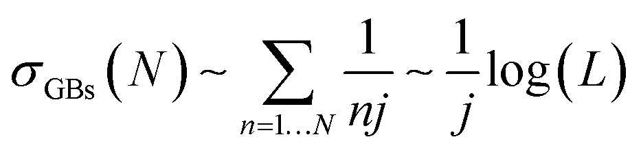
The stress accumulation (σGBs(L)) of GBs can be expressed by the following eqn (14):41
| |
 | (14) |
where
Nis 5|7 dislocation.
The stress accumulation (σholes(N)) of nanoholes can be expressed by the following eqn (15):
| |
 | (15) |
where
N is the dimension of nanoholes;
S is the number of nanoholes.
The stress accumulation (σFGOs(i)) of GBs can be expressed by the following eqn (16):
| |
 | (16) |
where
i are the hydroxyl, epoxy and their combination,
i = 1, 2, 3.
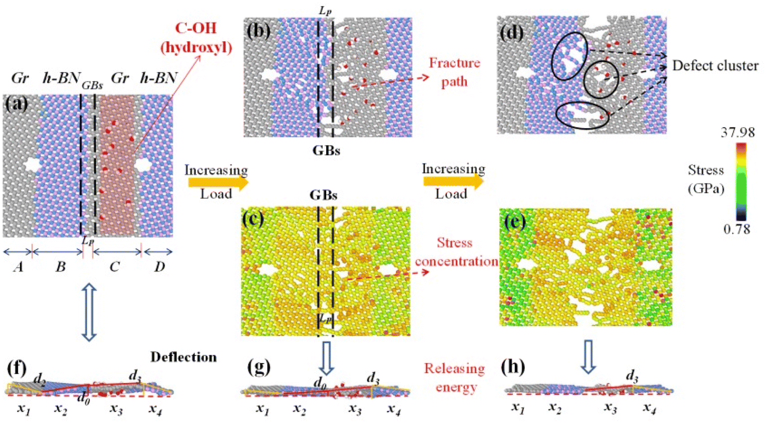
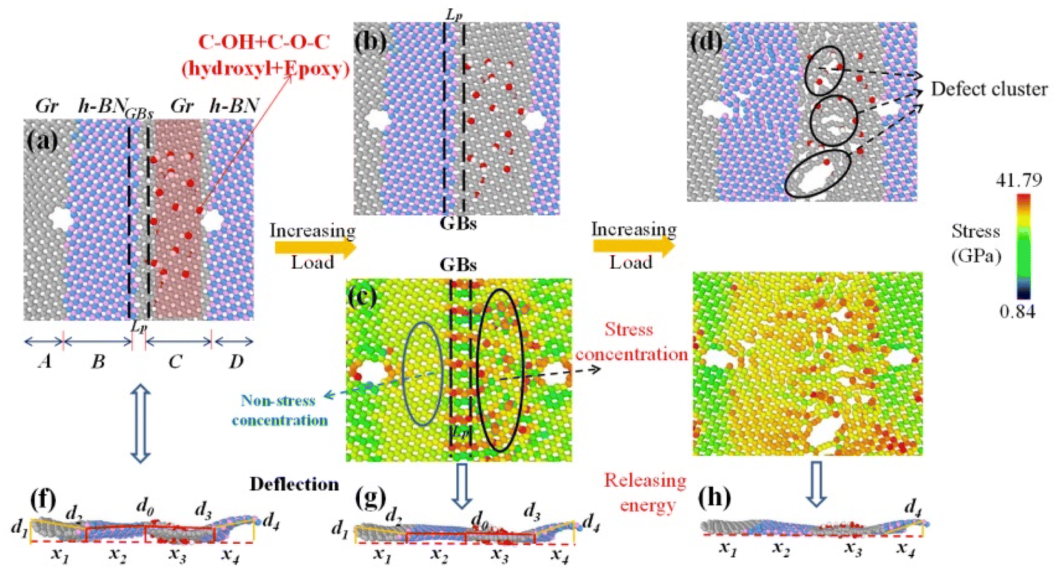
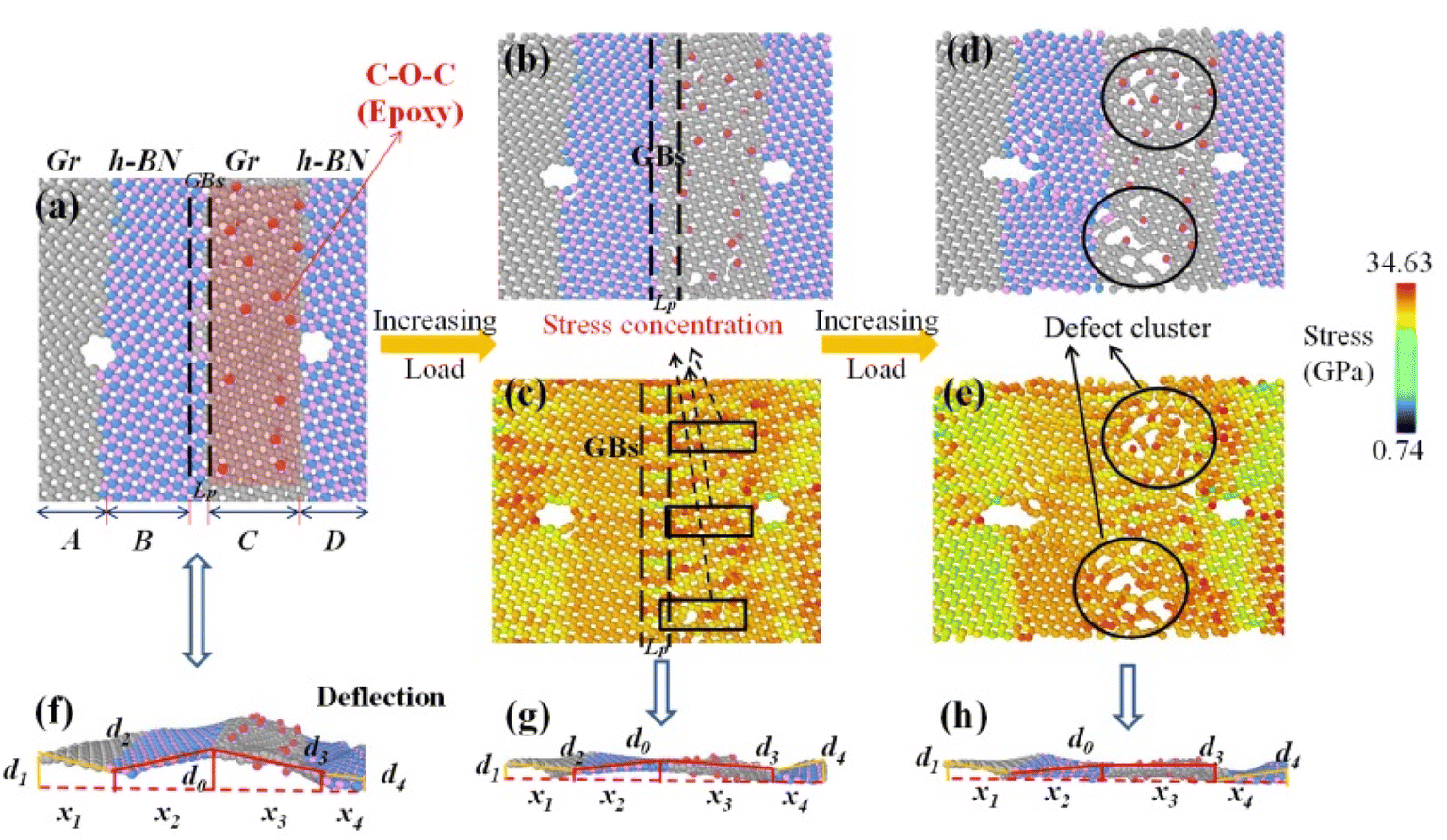
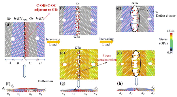
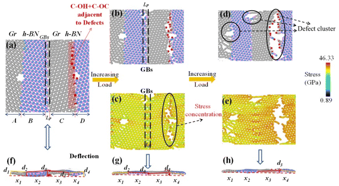
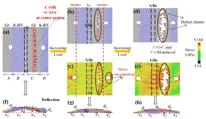
FGOs such as hydroxyl and epoxy groups are randomly or directional distributed on the surface of defective Gr–BN interface nanostructures. Different local distribution leads to different degrees of lattice distortion. It makes the surface of defective Gr–BN interface nanostructures show uneven fluctuation. Fig. 11–13(f) show the FGOs, GBs and nanoholes will induce defective Gr–BN interface nanostructures to deviate from the plane configuration, and produce saddle shapes with positive and negative curvatures. It is found from Fig. 5–7 that the crack position with the maximum strain energy and Von-mises stress always appears the accumulated stress domain (x3), while the defect clusters have not yet appeared in the non-accumulated stress domain (x2) and the built-in distorted stress domain (x1 and x4) (see Fig. 12 and 13(b and c)). With the increase of tensile strain, the bonding of atoms in the stress accumulation domain is incomplete, or the entropy of atoms is unstable, and the energy distribution is unbalanced. It makes the stress accumulation domain (x3) more prone to crack and connect many defects. Due to the continuous expansion of a single defect, the atomic stress distortion in the x3 domain is transferred to the adjacent area, and further defect clusters are formed (see Fig. 11–13(d and e). In addition, according the Von-mises stress theory, the lowest Von-mises stress for C–O–C groups, relative to C–OH + C–O–C and C–OH groups, can be attributed to the fact that the C–O–C groups has a lower binding energy and stability in stress accumulation domain (x3).
 |
| | Fig. 11 The geometrical deformation and stress distribution of a Gr–BN interface with hydroxyl groups, including (a and f) before cracking, (b, c and g) reaching the strain limit and (d, e and h) after cracking. | |
 |
| | Fig. 12 The geometrical deformation and stress distribution of a Gr–BN interface with hydroxyl and epoxy groups, including (a and f) before cracking, (b, c and g) reaching the strain limit and (d, e and h) after cracking. | |
 |
| | Fig. 13 The geometrical deformation and stress distribution of a Gr–BN interface with epoxy groups, including (a and f) before cracking, (b, c and g) reaching the strain limit and (d, e and h) after cracking. | |
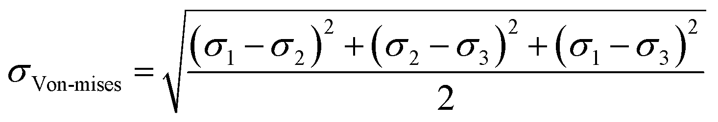
The Von-mises stresses were calculated by the following eqn (17):42
| |
 | (17) |
where
σ1,
σ2 and
σ3 are characteristic as the first, second principal and third stresses, respectively. It is assumed that the whole system has no shear stress.
The existence of GBs, nanoholes and FGOs changes the atoms arrangement and in-plane strain in the stress accumulation domain (x3), the non-accumulated stress domain (x2) and the built-in distorted stress domain (x1 and x4). Also, the out-of-plane deformation caused by geometrical effects also has an important impact on mechanical properties of Gr–BN interface nanostructures. Next, we turn our attention to the effect of GBs, FGOs and nanoholes on geometrical effects as well as the structural buckling at different domain.
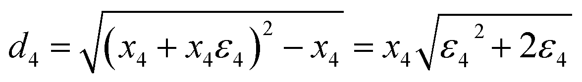
Geometrical effect and deflection (d) caused by strain of stress accumulation domain, non-accumulated stress domain and built-in distorted stress domain can also be calculated by the following formulas (18)–(21):
| |
 | (18) |
| |
 | (19) |
| |
 | (20) |
| |
 | (21) |
where
d1,
d2,
d3 and
d4 are displacement increment of deflection in.
x1,
x2,
x3 and
x4 domain, respectively.
It is also found that Gr–BN interface with FGOs nanostructures takes stress accumulation domain (x3) as the fulcrum, and the whole system presents different degrees of structural buckling. With the action of external force, the 2D planar configuration gradually changes to a negative Gaussian surface. The softening and weakening effects induced by GBs, nanoholes and FGOs are gradually enhanced. Clearly, the displacement increment of deflection d0 of the Gr–BN interface with C–O–C nanostructures at fulcrum locations is higher than that of other two types. In addition, the d3 of the Gr–BN interface with C–O–C nanostructures at stress accumulation domain (x3) (the weakest key areas) also shows highest structural buckling tendency. From the displacement increment of deflection differences between the C–O–C, C–OH and C–O–C + C–OH, a relatively small fraction of C–O–C groups can achieve higher displacement increment of deflection at the cost of a dramatically decrease in planar Von-mises stresses at stress accumulation domain (x3), non-accumulated stress domain (x2) and built-in distorted stress domain (x1 and x4).
3.6 Accumulated stress and decay-induced region via internal effects
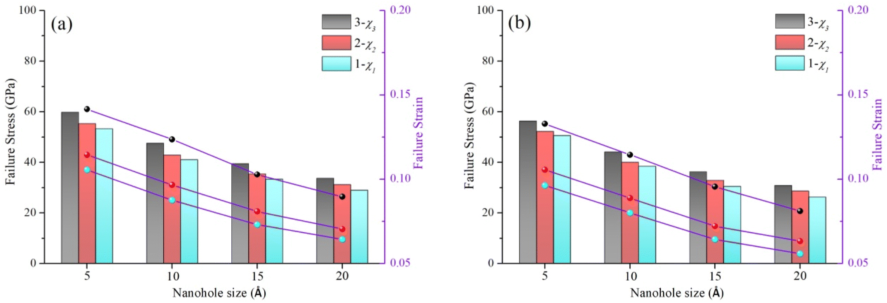
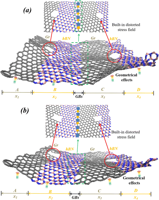
It is confirmed from the foregoing analysis that the interaction between GBs, nanoholes and FGOs affect the built-in distortion stresses. Moreover, the built-in distortion stresses also affect the geometrical buckling and stress accumulation of 2D materials. Next, FGOs-Nanoholes neighbor model (1−χ1), FGOs-GBs neighbor model (2−χ2) and FGOs central model (3−χ3) are created to investigate the transmission and decay effects of built-in distorted stress from one domain to another domain, as shown in Fig. 14(a–c). Fig. 14(a–c) contains the circular nanoholes, GBs and FGOs in Gr–BN interface nanostructures, and square nanoholes also created in system for comparison.
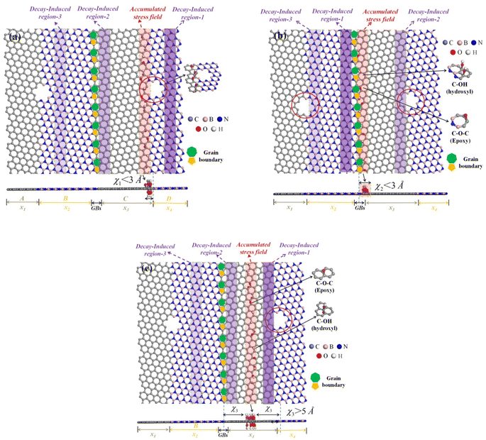 |
| | Fig. 14 The transmission and decay of built-in distortion stresses in 2D materials (a) FGOs-GBs neighbor model, (b) FGOs central model and (c) FGOs-nanoholes neighbor model. | |
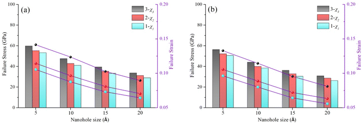
Fig. 15 shows the fracture strength and strain of FGOs-GBs neighbor model, FGOs central model and FGOs-nanoholes neighbor model. It is found that the fracture strength and strain of three models are significant reduced by increasing the nanoholes dimensions. Also, the lowest values for fracture strength and strain are achieved when the FGOs is adjacent to the nanoholes, while the highest values for fracture strength and strain are obtained when the FGOs is located at between nanoholes and GBs. Of course, in the FGOs central model (3−χ3), by adding the sizes of circular nanoholes from 5 to 20 Å, the fracture strength and strain of 3−χ3 model are reduced by 43.56% and 36.68%, respectively. However, in the FGOs-nanoholes neighbor model (1−χ1), the fracture strength and strain are reduced by 14.19% and 28.13% for the 20 Å square nanoholes, compared with 20 Å circular nanoholes.
 |
| | Fig. 15 The fracture strength and strain of FGOs-GBs neighbor model, FGOs central model and FGOs-nanoholes neighbor model. (a) Circular nanoholes in the models and (b) square nanoholes in the models. | |
Fig. (16–18) show the geometrical deformation and stress distribution of FGOs-GBs neighbor model, FGOs-GBs neighbor model and FGOs central model, respectively.
 |
| | Fig. 16 The geometrical deformation and stress distribution of FGOs-GBs neighbor model, including (a and f) before cracking, (b, c and g) reaching the strain limit and (d, e and h) after cracking. | |
 |
| | Fig. 17 The geometrical deformation and stress distribution of FGOs-nanoholes neighbor model, including (a and f) before cracking, (b, c and g) reaching the strain limit and (d, e and h) after cracking. | |
 |
| | Fig. 18 The geometrical deformation and stress distribution of FGOs central model, including (a and f) before cracking, (b, c and g) reaching the strain limit and (d, e and h) after cracking. | |
Next, we turn our attention to the FGOs-GBs neighbor model, the stress concentration mainly occurs at x3 domain, followed by x2 domain, x4 domain and x1 domain (see Fig. 16). Moreover, the corresponding displacement increment of deflection (d0 and d3) is highest at x3 domain, followed by d2, d4 and d1. With the increase of loading, the built-in distortion stress in x3 domain of FGOs-GBs neighbor model reaches the maximum value. Finally, the built-in stress field generated by GBs and FGOs is transferred to the x2 domain, x4 domain and x1 domain through covalent bond. Therefore, we can know that the interaction of defects is greater than that of a single defect. The values of the built-in distortion stress (induced by interaction of defects) decays with the increase of bonds distance. Similarly, the transmission and attenuation of the built-in distortion stress in other models also follow the regular tendency.
Defect interaction will not only affect the in-plane stress transfer, but also affect the out of plane stiffness of 2D materials.
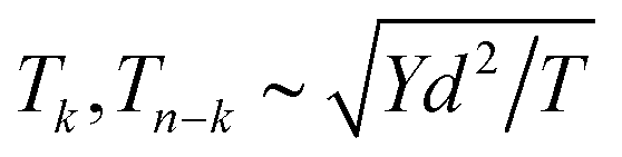
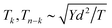
According to the theory of statistical mechanics, the structure with out-of-plane displacement (d) has the following scaling relationship with equivalent tensile force, in-plane Young's modulus, shear rigidities and bending rigidities:43
| |
 | (22) |
| |
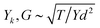 | (23) |
where
Tk is renormalized bending rigidities,
Tn−k is renormalized Gauss bending rigidities,
T is bending rigidities,
Y is regional Young's modulus,
G is shear rigidities and
Yk is renormalized Young's modulus.
On the basis of the previous analysis, it is found that the stress accumulation, transmission, attenuation and geometric effects of GBs, FGOs and nanoholes with distance have two opposite aspects. On one hand, for bridges with covalent bonds as stress transfer, the built-in distortion stress and regional Young's modulus decay with the distance of covalent bonds. On the other hand, the interactions of GBs, nanoholes and FGOs slightly enhance the bending rigidities of 2D materials due to their interactions induced out-plane deformation. In addition, because the 2D materials release energy in the process of tensile failure, the potential energy and deflection are reduced, while the defect energy is increased. Therefore, the negative effect of defect interactions on 2D materials is greater than the positive effect.
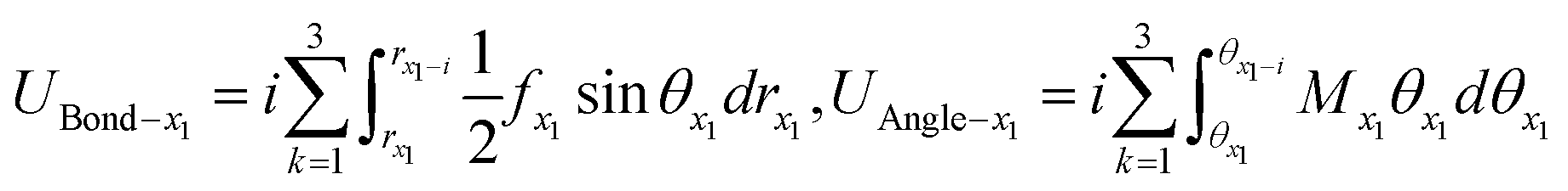
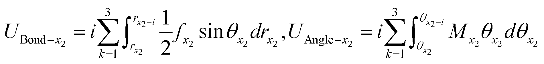
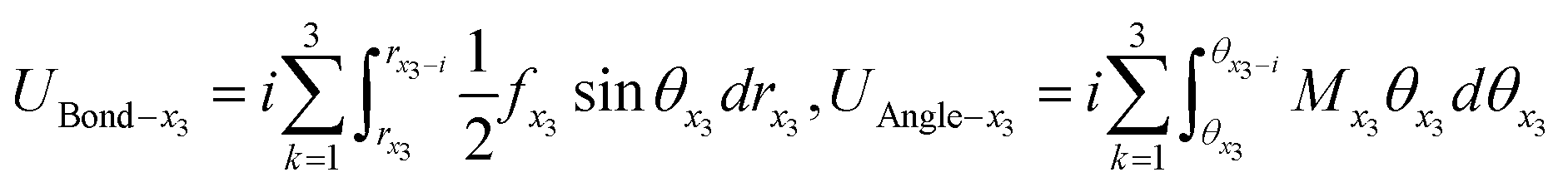
3.7 Bonding energy and length in internal effects (GBs, nanoholes and FGOs)
In order to study the changes of bond length, bond angle and its strain energy ratio in each domain of 2D materials, the strain energy (UBond and Uangle) induced by bond length and bond angle at x1, x2, x3 and x4 domain can be calculated by the following formulas (24)–(27):| |
 | (24) |
| |
 | (25) |
| |
 | (26) |
| |
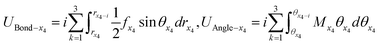 | (27) |
where UBond–x1, UBond–x1, UBond–x1 and UBond–x1 are strain energy of bond length change at x1, x2, x3 and x4 domain, respectively. UAngle–x1, UAngle–x2, UAngle–x3 and UAngle–x4 are strain energy of bond length change at x1, x2, x3 and x4 domain, respectively. rC0 represents the initial equilibrium bond length corresponding to the C atom of Gr; rB0 and rN0 represents the initial equilibrium bond length corresponding to the B and N atom of BN;θC0 is initial equilibrium bond length corresponding to the C atom of Gr; θB0 and θN0 is the initial equilibrium bond length corresponding to the B and N atom of BN; rCi, rBi and rNi indicate the bond length during stretching; θCi, θBi and θNi indicate the bond angle during stretching; f is the force on the covalent bond and M is the bending moment of the covalent bond angle.
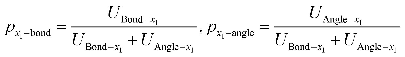
The effects of defects interaction on geometrical deformation by analyzing the change of bond length and bond angle in the proportion of strain energy are expressed by the following eqn (28)–(31):
| |
 | (28) |
| |
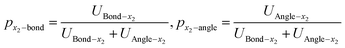 | (29) |
| |
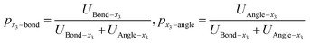 | (30) |
| |
 | (31) |
where
px1–bond and
px1–angle is the bond length and bond angle changes of
x1 domain in the proportion of strain energy;
px2–bond and
px2–angle is the bond length and bond angle changes of
x2 domain in the proportion of strain energy. The interpretation of strain energy in
x3 and
x4 domain are the same as above.
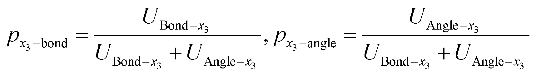
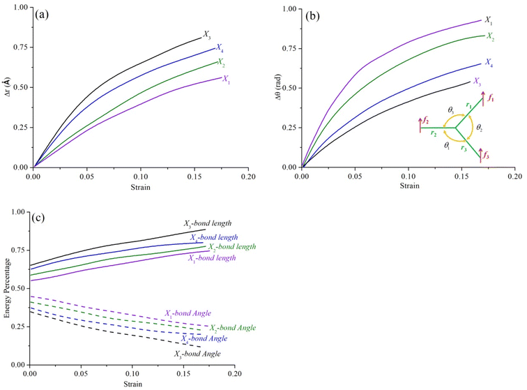
According to nonlinear mechanical theory and eqn (23)–(30), the changes of bond length, bond angle and its strain energy ratio in each domain of 2D materials are shown in Fig. 19. It is noted that the increment of bond length and bond angle are represented by Δr and Δθ, respectively. There are obvious differences in the change tendency of bond length and bond angle in each domain (x1,x2,x3 and x4) of 2D materials. Under the same strain, the change of bond length in the x3 domain is higher than that in other domain (x1, x2 and x4). On the contrary, the change curve of bond angle in the x1 domain is higher than that in other domain (x3, x2 and x4). Clearly, the distortion stress in x3 domain is greater than that of in x1, x2 and x4 domain. The bond angle change of x1 domain is obvious and plays a leading role in the stretching process, while the bond length change of x1 domain has a weak influence during the tension. Therefore, the x1 domain shows strong ductility, relative to other domain. In addition, The px1–bond increases gradually with the increase of strain, while px1–angle is gradually decreasing. Herein, it should be noted that in the initial tensile stage, the px3–bond at x3 domain is greater than the px1–bond at x1 domain, while the px3–angle at x3 domain is lower than the px1–bond at x1 domain. The ratio of strain energy (bond length and angle) is very sensitive to each domain of 2D materials. It explains why the same material itself has obvious regional characteristics (the differences of bond length, bond angle and its strain energy ratio). It is confirmed that geometrical effect, built-in distortion stress transfer and attenuation appeared in the order-disorder transition processes of 2D materials (see Fig. 20).
 |
| | Fig. 19 The changes of bond length, bond angle and its strain energy ratio in each domain of 2D materials. (a) Increment curves of bond length, (b) increment curves of bond angle and (c) ratio of strain energy (bond length and angle). | |
 |
| | Fig. 20 The built-in distortion stress transfer and attenuation of 2D materials during the order–disorder transition processes. (a) Geometrical effects induced by FGOs, nanoholes and GBs, (b) order transition processes and (c) disorder transition processes. | |
4 Conclusion
The GBs, nanoholes and FGOs in 2D materials will lead to geometrical deformation and related built-in distortion stress/strain. This kind of built-in distortion stress can lead to the secondary mechanical behaviors of 2D materials, such as sliding, buckling, folding, breaking and out-of-plane movement of 2D materials. It is directly coupled with the growth reaction, and then change the growth process of materials. By using molecular dynamics and nonlinear mechanics theory, a new model (combining both planar 2D heterostructures and GO) was established to study geometrical effects, stress accumulation, bonding energies and mechanical properties of 2D interface (key point) at stress distortion field, accumulated stress field and non-accumulated stress field. The results show that FGOs such as hydroxyl and epoxy groups are randomly or directionally distributed on the surface of defective Gr–BN interface nanostructures, and the difference of local distribution induces different degrees of lattice distortion. It makes the surface of defective Gr–BN interface nanostructures show uneven fluctuation. Moreover, the FGOs, GBs and nanoholes will induce defective Gr–BN interface nanostructures to deviate from the plane configuration, and produce saddle shapes with positive and negative curvatures, which have displacement fields diverging with distance. The internal field (defects, GBs and FGOs) affect the mechanical properties of Gr–BN interface nanostructures in two contrary ways. On one hand, the presence of internal field can lead to a reduction in the failure stress and strain. On the other hand, the presence of internal field changes spatial configuration and out-of-plane displacement. The flattening of out-of-plane displacement can significantly reduce the tensile ratio of covalent bonds, resulting in a significant increase of failure strain.
The built-in distortion stress field and geometric effect induced by defects will lead to richer growth morphology of 2D materials, and will also cause to more interesting scientific problems, which is expected to become a new growth point of 2D materials research in the future.
Abbreviations
| Gr | Graphene |
| FGOs | Functional group |
| 2D | Two-dimensional |
| MD | Molecular dynamics |
| GO | Graphene oxide |
| GBs | Grain boundary |
| C–OH | Hydroxyl |
| C–O–C | Epoxy |
| C–OH + C–O–C | Hydroxyl + epoxy |
| Gr–BN interface | Graphene–hBN–graphene–hBN |
| LAMMPS | Large-scale atomic/molecular massively parallel simulator |
| N | Nitrogen |
| B | Boron |
| C | Carbon |
| H | Hydrogen |
| O | Oxygen |
| GO–BN-C1 | Gr–BN interface with 10 Å circular nanohole, GBs and FGOs |
| GO–BN-C2 | Gr–BN interface with 20 Å circular nanohole, GBs and FGOs |
| GO–BN-S1 | Gr–BN interface with 10 Å square nanohole, GBs and FGOs |
| GO–BN-S2 | Gr–BN interface with 20 Å square nanohole, GBs and FGOs |
Conflicts of interest
No potential conflict of interest was reported by the authors.
Acknowledgements
This work was supported by a Doctoral program of Zhejiang University of science and technology (F701104L08).
References
- Z. G. Song and Z. P. Xu, Geometrical effect 'stiffens' graphene membrane at finite vacancy concentrations, Extreme Mechanics Letters, 2016, 6, 82–87 CrossRef.
- J. C. Meyer, A. K. Geim and M. I. Katsnelson, et al. The structure of suspended graphene sheets, Nature, 2007, 446, 60–63 CrossRef CAS PubMed.
- Z. Xu and M. J. Buehler, Geometry controls conformation of graphene sheets: Membranes, ribbons, and scrolls, ACS Nano, 2010, 4, 3869–3876 CrossRef CAS PubMed.
- G. López-Polín, C. Gomez-Navarro and V. Parente, et al. Increasing the elastic modulus of graphene by controlled defect creation, Nat. Phys., 2015, 11, 26–31 Search PubMed.
- Z. G. Song and Z. P. Xu, Topological defects in two-dimensional crystals: the stress buildup and accumulation, J. Appl. Mech., 2014, 81, 091004 CrossRef.
- T. Zhang, X. Li and H. Gao, Defects controlled wrinkling and topological design in graphene, J. Mech. Phys. Solid., 2014, 67, 2–13 CrossRef CAS.
- L. Fan, J. Xu and Y. H. Hong, Defects in graphene-based heterostructures: Topological and geometrical effects, RSC Adv., 2022, 12, 6772 RSC.
- Z. G. Song, V. I. Artyukhov and B. I. Yakobson, et al. Pseudo hall-petch strength reduction in polycrystalline graphene, Nano Lett., 2013, 13, 1829–1833 CrossRef CAS PubMed.
- J. Xu, X. Y. Cui, N. Liu, Y. N. Chen and H. W. Wang, Structural engineering of graphene for high-resolution cryo-electron microscopy, SmartMat, 2021, 2, 202–212 CrossRef CAS.
- Y. T. Niu, F. Z. Qing, X. S. Li and B. Peng, Inhomogeneous strain and doping of transferred CVD-grown graphene, Rare Met., 2022, 41(5), 1727–1734 CrossRef CAS.
- X. N. Hao and X. Liu, Molecular dynamics study on microscale residual stress of graphene/aluminum nanocomposites by selective laser sintering, Rare Met., 2022, 41(11), 3677–3683 CrossRef CAS.
- W. J. Yao and L. Fan, Research on the correlation of mechanical properties of BN–graphene–BN/BN vertically-stacked nanostructures in the presence of interlayer sp3 bonds and nanopores with temperature, Phys. Chem. Chem. Phys., 2020, 22, 5920 RSC.
- M. Y. Li, B. Zheng and K. Duan, et al. Effect of defects on the thermal transport across the graphene/hexagonal boron nitride interface, J. Phys. Chem. C, 2018, 122, 14945–14953 CrossRef CAS.
- Z. Zandiatashbar, G. H. Lee and S. J. An, et al. Effect of defects on the intrinsic strength and stiffness of graphene, Nat. Commun., 2014, 5, 3186 CrossRef PubMed.
- D. L. Nike and A. A. Balandin, Phonons and thermal transport in graphene and graphene-based materials, Rep. Prog. Phys., 2017, 80(3), 036502 CrossRef PubMed.
- L. Fan and W. J. Yao, Reduction of interfacial thermal transport of bilayer in-plane graphene/hexagonal boron nitride heterostructures via interlayer sp3 bonds and defects, Diamond Relat. Mater., 2021, 118, 108521 CrossRef CAS.
- J. W. Zhu, Y. P. Huang and W. C. Mei, et al. Effects of intrinsic pentagon defects on electrochemical reactivity of carbon nanomaterials, Angew. Chem., Int. Ed., 2019, 58(12), 3859–3864 CrossRef CAS PubMed.
- S. Korkmaz and I. A. Kariper, Graphene and graphene oxide based aerogels: Synthesis, characteristics and supercapacitor applications, J. Energy Storage, 2020, 27, 101038 CrossRef.
- L. Fan and W. J. Yao, Temperature dependence of interfacial bonding and configuration transition in graphene/hexagonal boron nitride containing grain boundaries and functional groups, Int. J. Mol. Sci., 2022, 23, 1433 CrossRef CAS PubMed.
- S. H. Zhu, Y. L. Gen and M. A. Yang, et al. Probing the intrinsic active sites of modified graphene oxide for aerobic benzylic alcohol oxidation, Appl. Catal. B Environ., 2017, 211, 89–97 CrossRef CAS.
- X. W. Chen, X. Hai and J. H. Wang, Graphene/graphene oxide and their derivatives in the separation/isolation and preconcentration of protein species: A review, Anal. Chim. Acta, 2016, 922, 1–10 CrossRef CAS PubMed.
- A. T. Dideikin and A. Y. Vul, Graphene oxide and derivatives: The place in graphene family, Frontiers in Physics, 2019, 6, 149 CrossRef.
- R. K. Joshi, S. Alwarappan and M. Yoshimura, Graphene oxide: the new membrane material, Appl. Mater. Today, 2015, 1(1), 1–12 CrossRef.
- C. Chang, Z. G. Song and J. Lin, et al. How graphene crumples are stabilized?, RSC Adv., 2013, 3, 2720–2726 RSC.
- X. J. Liu, G. Zhang and Y. W. Zhang, Topological defects at the graphene/h-BN interface abnormally enhance its thermal conductance, Nano Lett., 2016, 16, 4954–4959 CrossRef CAS PubMed.
- E. E. Kasra, S. Sadegh and J. Maisam, Mechanical properties of defective hybrid graphene-boron nitride nanosheets: A molecular dynamics study, Comput. Mater. Sci., 2018, 149, 170–181 CrossRef.
- L. Fan and W. J. Yao, Effects of vacancy defects on the mechanical properties of graphene/hexagonal BN superlattice nanoribbons, N. Carbon Mater., 2020, 35(2), 2165–2174 Search PubMed.
- V. Akarsh and P. Avinash, Molecular dynamics based simulations to study the fracture strength of monolayer graphene oxide, Nanotechnology, 2018, 29, 115706 CrossRef PubMed.
- T. Liang, T. R. Shan, Y. T. Cheng, B. D. Devine, M. Noordhoek, Y. Z. Li, Z. Z. Lu, S. R. Phillpot and S. B. Sinnott, Classical atomistic simulations of surfaces and heterogeneous interfaces with the charge-optimized many body (COMB) potentials, Mater. Sci. Eng. R Rep., 2013, 74, 255–279 CrossRef.
- L. Deng and J. C. Du, Development of boron oxide potentials for computer simulations of multicomponent oxide glasses, J. Am. Ceram. Soc., 2019, 102, 2482–2505 CrossRef CAS.
- B. B. Sharma and A. Parashar, Atomistic simulations to study the effect of water molecules on the mechanical behavior of functionalized and non-functionalized boron nitride nanosheets, Comput. Mater. Sci., 2019, 169, 109092 CrossRef CAS.
- N. Chandra, S. Namilae and C. Shet, Local elastic properties of carbon nanotubes in the presence of Stone-Wales defects, Phys. Rev. B, 2004, 69, 094101 CrossRef.
- F. Liu, P. M. Ming and J. Li, Ab initio calculation of ideal strength and phonon instability of graphene under tension, Phys. Rev. B, 2007, 76, 064120 CrossRef.
- C. Lee, X. D. Wei, J. W. Kysar and J. Hone, Measurement of the elastic properties and intrinsic strength of monolayer graphene, Science, 2008, 321, 385–388 CrossRef CAS PubMed.
- N. Ding, X. F. Chen and C. M. L. Wu, Mechanical properties and failure behaviors of the interface of hybrid graphene/hexagonal boron nitride sheets, Sci. Rep., 2016, 6, 31499 CrossRef CAS PubMed.
- A. Bosak, J. Serrano, M. Krisch, K. Watanabe, T. Taniguchi and H. Kanda, Elasticity of hexagonal boron nitride: inelastic X-ray scattering measurements, Phys. Rev. B, 2006, 73, 041402 CrossRef.
- E. E. Kasra, S. Sadegh and J. Maisam, The mechanical design of hybrid graphene/boron nitride nanotransistors: Geometry and interface effects, Solid State Commun., 2018, 270, 82–86 CrossRef.
- L. Fan, K. Liu, G. Y. Liu and Y. H. Hong, Defects in Gr/h-BN nanoribbons heterostructure: Atomically precise cutting and defect amplification effect via hydrogenation pseudo-crack, Diamond Relat. Mater., 2022, 123, 108877 CrossRef CAS.
- L. Fan, W. J. Yao and Z. P. Zhang, Regulation of failure mechanism of a bilayer Gr/h BN staggered stacked heterostructure via interlayer sp 3 bonds, interface connection, and defects, Appl. Phys. A: Mater. Sci. Process., 2020, 126, 752 CrossRef CAS.
- Y. F. Li, A. R. Wei, H. Ye and H. M Yao, Mechanical and thermal properties of grain boundary in a planar heterostructure of graphene and hexagonal boron nitride, Nanoscale, 2018, 10, 3497 RSC.
- M. J. Alava, P. K. V. Nukala and S. Zapperi, Statistical models of fracture, Adv. Phys., 2006, 55, 349–476 CrossRef.
- K. E. Eshkalak, S. Sadeghzadeh and M. Jalaly, Studying the effects of longitudinal and transverse defects on the failure of hybrid graphene-boron
nitride sheets: A molecular dynamics simulation, Phys. E Low-dimens. Syst. Nanostruct., 2018, 104, 71–81 CrossRef CAS.
- A. Kosmrlj and D. R. Nelson, Mechanical properties of warped membranes, Phys. Rev. E, 2013, 88(1), 012136 CrossRef PubMed.
Footnote |
| † These authors contributed equally to this work. |
|
| This journal is © The Royal Society of Chemistry 2022 |
Click here to see how this site uses Cookies. View our privacy policy here. 
 Open Access Article
 This Open Access Article is licensed under a Creative Commons Attribution-Non Commercial 3.0 Unported Licence
 *a,
Xinyu Cai†*b,
Hongwei Wanga,
Jian Yea,
Yong Fenga,
Zhuye Huanga and
Chen Qu*a
*a,
Xinyu Cai†*b,
Hongwei Wanga,
Jian Yea,
Yong Fenga,
Zhuye Huanga and
Chen Qu*a