DOI:
10.1039/D2RA06303D
(Review Article)
RSC Adv., 2022,
12, 32853-32884
Copper oxide nanostructured thin films processed by SILAR for optoelectronic applications
Received
7th October 2022
, Accepted 9th November 2022
First published on 16th November 2022
Abstract
The lack of high-functioning p-type semiconductor oxide material is one of the critical challenges that face the widespread performance of transparent and flexible electronics. CuxO nanostructured thin films are potentially appealing materials for such applications because of their innate p-type semi-conductivity, transparency, non-toxicity, abundant availability, and low-cost fabrication. This review summarizes current research on CuxO nanostructured thin films deposited by the SILAR technique. After a brief introduction to the advantages of CuxO semiconductor material, diverse approaches for depositing and growing such thin films are discussed. SILAR is one of the simplest deposition techniques in terms of better flexibility of the substrate choice, the capability of large-area fabrication, budget-friendly, deposition of stable and adherent film, low processing temperature for the film fabrication as well as reproducibility. In addition, various fabrication parameters such as types of copper salts, pH of precursors, number of cycles during immersion, annealing of as-deposited films, doping by diverse dopants, and growth temperature affect the rate of fabrication with the structural, electrical, and optical properties of CuxO nanostructured thin films, which led the technique unique to study extensively. This review will include the recent progress that has recently been made in different aspects of CuxO processed by the SILAR. It will describe the theory, mechanism, and factors affecting SILAR-deposited CuxO. Finally, conclusions and perspectives concerning the use of CuxO materials in optoelectronic devices will be visualized.
1. Introduction
1.1 Background
Copper (Cu) and copper oxide (CuxO) thin films have been studied extensively due to their potential application in semiconductor technology long before the Ge and Si era started, and researchers have faced much more difficult to work with this oldest material ever. The n-type window layer semiconductors such as ZnO, ITO, FTO, and GaN with large bandgap energies have already achieved outstanding optical as well as electronic transport properties. Consequently, the effort of detecting new, prospective p-type absorber layers for optoelectronics devices has led to intensive research.
CuxO semiconductors are very attractive and have been broadly studied in both theoretical analysis and investigations into applied executions of nano or optoelectronic devices due to their chemically stable nature, nontoxicity, relative abundance, potential particle size effects, excellent performance as a catalyst, and fulfill all the requirements for low-cost manufacturing at ambient conditions, which have high potential usage in energy storage, conversion, and next-generation rechargeable lithium-ion batteries.1–6 Furthermore, CuxO nanostructures are extensively used in other diverse applications, including photovoltaics,7 photodetectors,8 nanofluid,9,10 energetic materials,11 field emissions,12 supercapacitors,13,14 biosensors,15,16 gas sensors,17,18 photocatalysis,19,20 removal of inorganic pollutants,21,22 and magnetic storage media.23,24
Both the Cu2O and CuO show direct transition nature with a direct band gap of around 2.1 and 1.5 respectively, having a high extension coefficient of above 105 cm−1. Since the theoretical limit of the energy conversion efficiency of Cu2O and CuO is as high as 20 and 29%, respectively under air mass (AM) 1.5 solar illumination, numerous efforts were done to increase the efficiency of CuxO solar cells, but the performance remains very poor.25 In the case of Cu2O solar cells, it is not more than 8.1%,7 whereas in the case of CuO it is lower and still about 3%.26 Toward the large area fabrication, it is crucial to establish the thin film growth technique for CuxO. Thus, the research of CuxO thin films has both high-tech and scientific consequences.
CuxO nanostructured thin films have been synthesized by various approaches like electrodeposition,27 electron beam evaporation,28 magnetron sputtering,29–31 molecular beam epitaxy,32 sol–gel,33 solution growth,34 spin coating,35 successive ionic layer adsorption and reaction (SILAR),36,37 thermal evaporation,38 and vapor deposition.39 Among all the deposition methods, SILAR is one of the simplest methods in terms of better flexibility on substrate choice, the capability of large area fabrication and deposition of the stable and adherent film, low processing temperature for film fabrication as well as reproducibility.40 This technique is very budget friendly since it does not require any sophisticated equipment. Moreover, various fabrication parameters such as pH, annealing temperature and time, doping elements, the concentration of precursor solutions, and temperature of the precursor solutions affect the rate of fabrication as well as the structural, optical, and electrical properties of the fabricated thin films led the technique unique to study in an extensive manner.
More than a few reviews of different aspects of CuxO-based optoelectronics have been published based on the fabrication technique but still no such report for the SILAR technique. This paper concerns the progress that has recently been made in diverse aspects of CuxO-based thin films processed by the SILAR method, following the introduction in section one, several deposition techniques are reviewed in section two. The third section of this paper describes the theory and mechanism of CuxO-based thin films fabricated by the SILAR method. The fourth section, which incorporated the core focus of this review, leads to the factors that affect SILAR-based CuxO deposition which is followed by the application of CuxO in section five. Finally, conclusions and perspectives concerning the use of CuxO in optoelectronic devices are presented.
1.2 Properties of copper oxides (CuxO)
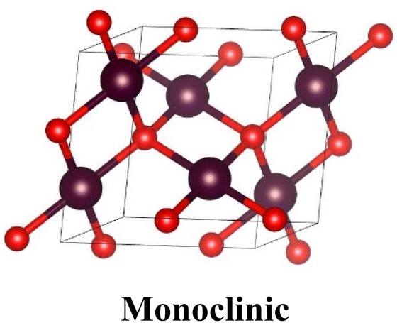
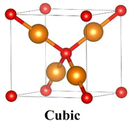
Cu2O exists as a simple cubic Bravais lattice8–10 with a space group of (Pn3m) or (O4h). Each unit cell consists of six atoms, the four Cu atoms are in a face-centered cubic lattice while the two O atoms are at the tetrahedral positions creating a body-centered cubic sublattice. Thus, O atoms are fourfold coordinated with Cu atoms as closest neighbors, and Cu atoms are linearly coordinated with two O atoms as closest neighbors as shown in Table 1. On the other hand, the unit cell of CuO fits into a monoclinic structure with the space group C2/c and the lattice parameters are represented in the table (PDF No. 89-5898). In each CuO unit, there exist four Cu–O bonds. As demonstrated in the table, in a unit, each Cu atom is surrounded by the four closest coplanar O atoms. The four O atoms are positioned at the angles of an almost rectangular parallelogram, which then unites another two O atoms to shape a highly distorted octahedron. The O atom is enclosed by the four closest Cu atoms positioned at the angle of a tetrahedron.
Table 1 Crystallographic properties of Cu2O and CuO41
| Parameters |
Cu2O |
CuO |
| Structure: Cu(I)-yellowish, Cu(II)-greyish black, O-red |
 |
 |
| Unit cell |
a = b = c = 4.26 Å |
a = 4.6837 Å, b = 3.4226 Å, c = 5.1288 Å |
| α = β = γ = 90° |
α, γ = 90°, β = 99.54° |
| Space group |
Pn![[3 with combining macron]](https://www.rsc.org/images/entities/char_0033_0304.gif) m (224) m (224) |
C2/c (15) |
| Bond length, Å |
Cu–O |
1.849 |
1.96 |
| O–O |
3.68 |
2.62 |
| Cu–Cu |
3.012 |
2.90 |
| Cell volume, Å3 |
77.83 |
81.08 |
| Formula weight |
143.14 |
79.57 |
| Density, g cm−3 |
5.749–6.140 |
6.515 |
| Melting point, °C |
1235 |
1201 |
1.3 Band-structure calculation
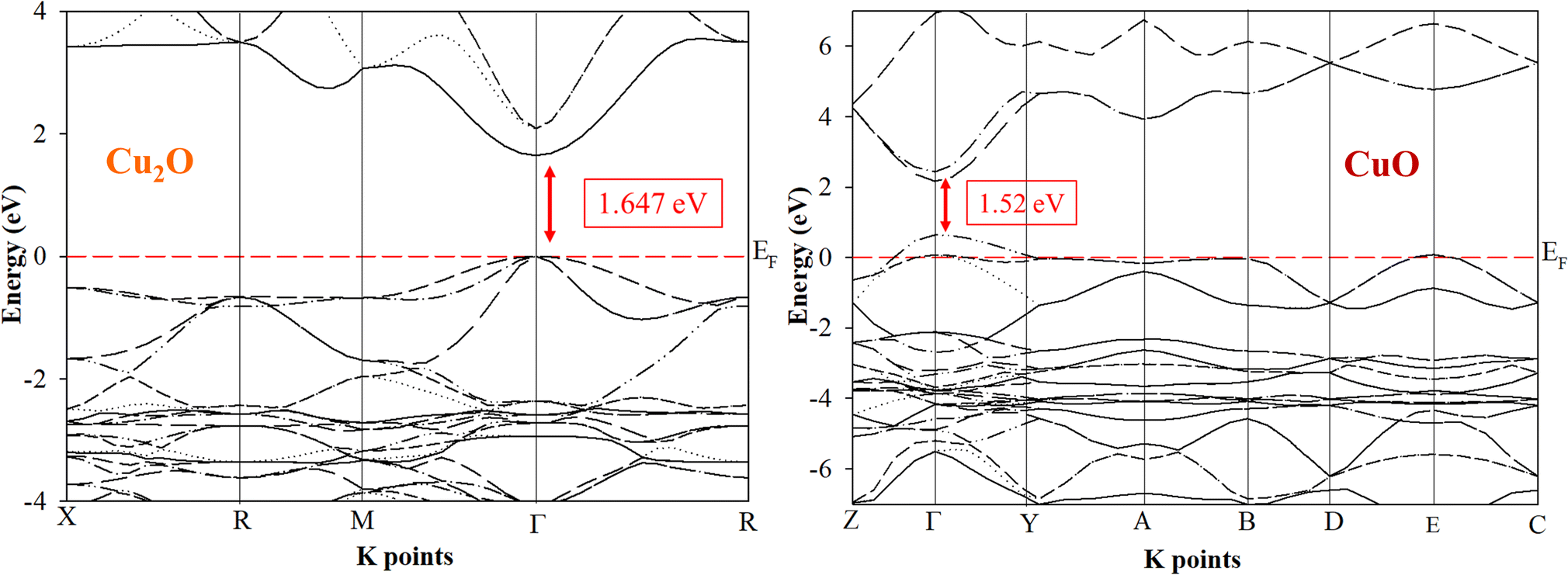
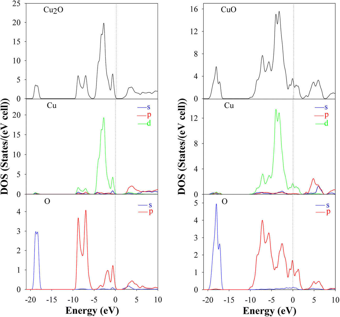
Ab initio calculations are mandatory to understand the optical and electronic properties of the CuxO systems. But there is a challenge for standard ab initio investigations based on DFT for both Cu2O and CuO. The exchange–correlation function is the crucial ingredient in the theoretical description. Fig. 1 and 2 represent the band structures, density of states (DOS), and partial density of states (PDOS) of the Cu2O and CuO compounds. The results were simulated for both Cu2O and CuO unit cells using CASTEP software within the LDA + U and the calculated bandgaps were found as 1.647 and 1.52 eV respectively.42
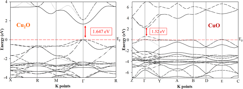 |
| | Fig. 1 Band structures of Cu2O and CuO unit cells are drawn by CASTEP using LDA + U. | |
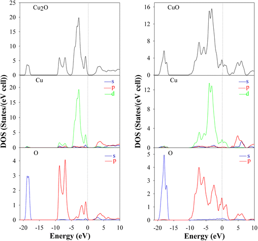 |
| | Fig. 2 DOS and PDOS of Cu2O and CuO unit cells are drawn by CASTEP using LDA + U. | |
2. Thin film deposition process
2.1 Physical deposition methods
The physical deposition methods have diverse techniques to attain thin films with good quality. It can be summarized with the raw materials, deposition conditions as well as cost of production as shown in Table 2.
Table 2 Physical deposition techniques with the requirements during deposition
| Physical deposition |
| Techniques |
Raw materials |
Conditions |
Substrate |
Film quality |
Budget |
Ref. |
| Thermal evaporation |
Red Cu2O powder |
Base pressure: 5 × 10⁻⁴ Pa |
Glass tantalum SiO2 |
— |
High |
43 |
| Temperature: 300 °C |
| Annealing temperature: 500 °C |
| Electron beam evaporation |
Cu2O pellets |
Deposition time: 5–16 min |
Glass |
Moderate |
High |
44 |
| Substrate temperature: 200 °C |
| Accelerating voltage: 2, 4 and 6 kV |
| Evaporation pressure: 3 × 10⁻² Pa |
| Ultimate pressure: 4 × 10⁻⁴ Pa |
| Filament current: 30 mA |
| Pulsed laser deposition |
Cu, O2 |
Substrate temperature: 25–400 °C |
Quartz ITO NaCl |
Excellent |
High |
45 |
| pO2: 0–10 mTorr |
| Vacuum chamber pressure: Torr |
| Molecular beam epitaxy |
Cu, O2 |
Incident O+ beam energy: 50 eV |
MgO |
Excellent |
High |
46 |
| Substrate temperature: 100–400 °C |
| Cu flux: 2.5 × 10¹³ to 1.6 × 10¹⁴ atoms per cm2 s |
| Base pressure: 3 × 10⁻¹⁰ torr |
| Total pressure: 3 × 10⁻⁹ to 2 × 10⁻⁸ |
| O+ flux: 2.7 × 10¹⁴ atoms per cm2 s |
| Ion plating evaporation |
Cu, O2 |
Base pressure: 10−4 Pa |
Glass |
Excellent |
High |
47 |
| O2 flow rate: 15–45 sccm |
| N2 flow rate: 0–6 sccm |
| RF power: 300 W |
| Annealing temperature: 300 °C |
| Substrate temperature: 25 °C |
| Direct current (DC) sputtering |
Cu, O2 |
Deposition pressure: 6.3 × 10⁻³ torr |
Glass |
Excellent |
High |
48 and 49 |
| Base pressure: 6 × 10⁻⁶ torr |
| Sputtering power: 60 W |
| Ar gas pressure: 20 sccm |
| pO2: 8.0 × 10⁻⁴ to 1.8 × 10⁻³ torr |
| Cu, O2 |
Sputtering power: 10–40 W |
Glass stainless steel |
| Ar flow rate: 15 sccm |
| O2 flow rate: 10 sccm |
| Substrate temperature: 300 °C |
| Ambient gas pressure: 0.045 Pa |
| Radio frequency (RF) sputtering |
Cu, O2 |
Substrate temperature: 300 °C |
Glass |
Excellent |
High |
50 |
| Ar flow rate: 10 sccm |
| O2 flow rate: 0–2 sccm |
| Deposition time: 60 min |
| Background pressure: <3 × 10⁻⁴ Pa |
| Working pressure: 1.7–1.8 Pa |
2.2 Chemical deposition methods
Likewise, diverse chemical deposition techniques with the deposition condition, raw materials, cost of production, the usual use of substrate etc. are discussed in Table 3 as shown below:
Table 3 Chemical deposition techniques with the requirements during deposition
| Techniques |
Raw materials |
Chemical deposition |
Substrate |
Film quality |
Budget |
Ref. |
| Conditions |
| Sol–gel |
CuCl2·2H2O, CH3OH, (CH2CH2OH)NH, glucopone, ethylene glycol |
Rotating speed: 2000 rpm |
TiO2 |
Good |
Low |
51 and 52 |
| Annealing temperature: 200–400 °C |
| Cu(II) acetate, H2N(CH2)2OH, 2-methoxyethanol, poly (ethylene glycol) |
Rotating speed: 1000 and 1500 rpm |
FTO Si |
| Annealing temperature: 350, 500 °C |
| Chemical bath deposition |
Cu(NO3)2·3H2O, triethanolamine, hydrazine hydrate |
Temperature: 30 °C |
Glass |
Excellent |
Low |
53 and 54 |
| Cu, HNO3, HF, C2H5OH, Na2SO4, CH3COCH3 |
Temperature: 30 °C |
Cu |
Molar ratio: HNO3![[thin space (1/6-em)]](https://www.rsc.org/images/entities/char_2009.gif) :HF-10:1 to 135:1 :HF-10:1 to 135:1 |
| HNO3 conc: 0–1.2 mmol L−1 |
| Water bath time: 2–6 days |
| Water-bath temperature: 10–45 °C |
| SILAR |
CuSO4·5H2O, NaOH, Na2S2O3·5H2O |
Temperature: 70 °C |
Glass FTO |
Excellent |
Low |
36 and 37 |
| pH: 2.35–7.33 |
| CuSO4·5H2O, NaOH, Na2S2O3·5H2O |
Temperature: 70 °C |
Glass FTO |
| pH: 4.50–7.95 |
| No. of cycles: 20–80 |
| Annealing temperature: 75–350 °C |
| Spray pyrolysis |
Cu(CH3COO)2·H2O, (CH3)2CHOH, C6H12O6 |
Temperature: 200–350 °C |
Glass |
Excellent |
Low |
55 and 56 |
| Deposition time: 45 min |
| No. of cycles: 450 |
| Cu(CH3COO)2·H2O, C6H12O6, (CH3)2CHOH |
Temperature: 200–350 °C |
Glass |
| Glucose conc: 0–0.08 M |
| Isopropanol volume (%): 0–100 |
| Cu salt conc: 0–0.08 M |
| Electrodeposition |
CuSO4·5H2O, lactic acid, NaOH |
Temperature: 30 and 60 °C |
Ti |
Excellent |
Low |
57–60 |
| pH: 9, 12 |
| Applied potential: −150 to −800 mV |
| CuSO4·5H2O, tri-sodium citrate dehydrate, C6H5Na3O7; KOH |
pH: 11 |
FTO |
| Time: 20–60 min |
| Applied potential: −0.4 V |
| Temperature: 30 °C |
| Cu(CH3COO)2·H2O, CH3COONa·3H2O |
Temperature: 20–80 °C |
ITO |
| Time: 2–80 min |
| NaCl conc: 1–10 mM |
| Potential: −0.1 to −0.4 V |
| Cupric acetate, sodium acetate, CH3COOH, NaOH |
Temperature: 20, 55 °C |
Ti ITO Pt |
| Deposition time: 45 min |
| pH: 5.4–7.49 |
| Applied potential: −200 to −400 mV |
| Cu(II) acetate con.: 0–16 mM |
| Chemical vapor deposition (CVD) |
Cu dipivaloylmethanate, Cu(C11H9O2)2; O2 |
O2 flow rate: 1 and 300 cm3 min−1 |
Borosilicate glass |
Excellent |
High |
61–63 |
| pO2: 1.689 × 10² and 5.07 × 10⁴ Pa |
| Temperature: 300 and 500 °C |
| N,N′-di-sec-butylacetamidinato)Cu(I), Cu-(sec-Bu-Me-amd)]2; DI H2O |
Substrate temperature: 125–225 °C |
Si waferGlassy carbon SiO2 glass |
| Process pressure: 1–10 torr |
| Vapor flow rate: 5 sccm |
| N2 flow rate: 100 sccm |
| Cu(II) acetylacetonate, Cu(C5H7O2)2; O2 |
Pressure: 5–200 sccm |
Sapphire MgO |
| Temperature: 350–500 °C |
| Atomic layer deposition (ALD) |
Cu(CH3COO)2·H2O, Cu(CH3COO)2, H2O vapor |
Temperature: 180–220 °C |
Glass Si |
Excellent |
High |
64 and 65 |
| Rector pressure: 10 mbar |
| N2, H2O and O2 flow rate: 400 sccm |
| Deposition cycles: 500–7000 |
| Cu(II)-bis-(dimethylamino-2-propoxide), O3 |
pO2: 34 Pa |
SiO2/Si |
| Substrate temperature: 112–165 °C |
| Deposition cycles: 500–10000 |
2.3 Advantages and disadvantages of deposition techniques
Till now, a lot of deposition techniques are available to fabricate high-quality thin films having diverse applications. For a better understanding, the advantages, and disadvantages of some of the chemical deposition techniques such as chemical bath deposition (CBD), atomic layer deposition (ALD) as well as spin coating are summarized to understand the potentiality of the SILAR method in Table 4.
Table 4 Involved advantages and disadvantages of the deposition techniques
| Techniques |
Merits |
Demerits |
| CBD |
Simple and cost effective |
Precipitation occurs in the bath causing serious problems |
| Stoichiometric deposition66 |
Materials are lost70 |
| Low fabrication temperature |
Films are badly cohered onto the substrate |
| Capability of depositing large area films (∼10 cm2)67 |
Produces powdery films |
| Various types of substrates are used68 |
Failed to control film thickness |
| Tuning film qualities by controlling growth parameters |
Deposited films are contaminated though organic additives |
| Deposition of ternary and quaternary compounds69 |
Opposite ions present in the reaction bath |
| SILAR |
Facile and economical |
Perfect adsorption of ions requires on the substrate surface |
| Potentiality to grow large-surface films (∼10 cm2)71 |
Substrate surface must be balanced completely through precursor solution73 |
| Reproducibility |
| Any kind of substrate can be used |
| No need to use sophisticated instrument or vacuum pump |
| No precipitation occurs in the bath |
| Synthesis of doped, ternary, and quaternary compounds |
| Does not need premium quality target |
| Controlling on film thickness |
| Avoid unnecessary heating |
| Minimization of dislocation density by controlling deposition parameters72 |
| Fabricated stable and sticky films36 |
| ALD |
Films thicknesses are under controlled |
Sluggish deposition process |
| Layer by layer film deposition |
Highly refined substrate is required |
| Deposition can be performed at relatively low temperature |
Instrument and substrate are highly priced |
| Soft substrates can be used |
Several trials required to set optimize film growth condition |
| Ability to use thermally unstable precursors due to slow degradation74,75 |
Process is restricted to non-volatile compounds |
| Unfavorable for heat sensitive biological substrates76,77 |
| Spin coating |
Dominated over film thicknesses |
Hindered to use multiple substrates at a time |
| Easy and effortless |
Restricted to utilize big substrate |
| Affordable |
Low material productivity |
| Fabricated stable cohered films |
Inexpensive with respect to photoresist and substrate size |
| Deficit of coupled variables |
95–98% materials are wasted80 |
| Reproducibility78,79 |
Less effective in nanotechnology due to quick drying81 |
| Solvothermal |
Dominate over crystallinity of the deposited films |
Requirement of expensive autoclave |
| Produces intermediate to specific quality films |
Safety issues |
| Potentiality to synthesize solid-state materials |
Impossible to observe in situ reaction process82 |
| Less dominance over particle size83 |
3. Theory and mechanism of SILAR process
SILAR is an extensively applied technique to fabricate high-quality metal oxide or halide thin films.84,85 During deposition, successive ionic layer adsorption and reaction of the ions take place at the solid–solution interface of the substrate. Thus, the thin film of the compound, AxBy is deposited onto the substrate surface by dint of the adsorbed cations, xAp+ and anions, yBq− due to the following heterogeneous chemical reaction:
| x[A(Ln)]p+ + pPx− + qQy+ + yBq− → AxBy + qQy+ + pPx− |
where, x, p, q, y and p+, x−, y+, q− are the number and charges of the corresponding ions A (metal ions), P (cationic precursor), Q (anionic precursor) and B (anions) respectively.85,86 Sometimes, the ligands, Ln are a necessity to complete the reaction.87–90
In the case of CuxO film deposition mechanism, salts of Cu2+ are used to deposit copper oxide thin films. In most of the research on Cu2O, firstly copper(I) thiosulfate complex is formed by the redox reaction between Cu2+ and S2O32− ions which results in a colorless solution. The corresponding reactions are:
Oxidation half-reaction:
Reduction half-reaction:
Overall reaction:
| 2Cu2+ + 4S2O32− → 2[Cu(S2O3)]− + S4O62− |
In the above reactions, [Cu(S2O3)]− the complex solution is regarded as the cationic precursor solution (cold solution) while NaOH is the anionic precursor solution, which is being kept at 70 °C (hot solution).91 When the substrate is immersed in the hot solution, OH− ions are adsorbed onto the substrate and subsequently dipping into the cold solution results in the adsorption of Cu+ ions. Thus, one SILAR cycle is completed and Cu2O thin film is formed due to the reaction between Cu+ and OH− ions. Rinsing is carried out after every immersion to exclude loosely adhered particles. The number of cycles as well as dipping time varies based on required film thicknesses. Corresponding reactions are given below 92 and the growth mechanism is schematically represented in Chart 1.
| [Cu(S2O3)]− → Cu+ + 2S2O32− |
| 2Cu+ + 2OH− → Cu2O(s) + H2O |
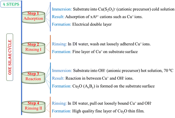 |
| | Chart 1 Representation of different steps during a SILAR cycle. | |
Therefore, a basic SILAR cycle comprises four different steps. The steps are represented in the following chart:
Consequently, a SILAR cycle covers four diverse steps on the surface, associating alternative immersion of the substrate into cationic and anionic precursor solution followed by rinsing in each immersion cycle to remove loosely adhered particles as demonstrated in Chart 2 and discussed below:
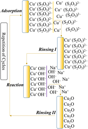 |
| | Chart 2 Schematic presentation of the deposited Cu2O nanostructured films on the substrate surface during a SILAR cycle. | |
3.1 Adsorption
First SILAR stage forms the Helmholtz double layer owing to the initial adsorption of the cationic precursor such as Cu+ on the substrate surface. This layer is generally composed of two charged layers, the positively charged, Cu+, inner layer and the negatively charged, (S2O3)2−, outer layers.
3.2 Rinsing I
In the second stage, extra adsorbed ions, Cu+ and (S2O3)2−, are rinsed away from the diffusion layer towards the bulk solution and a hypothetical monolayer is formed, resulting in a saturated electrical double layer.
3.3 Reaction
In the reaction step, the anions, OH−, from the anionic precursor solution are entered into the scheme. A solid substance, Cu2O, is synthesized on the interface due to the low stability of the material. This procedure pays the reaction of Cu+ species with the anionic precursor such as OH−.
3.4 Rinsing II
In the final SILAR cycle, the extra and unreacted species such as (S2O3)2−, Na+ as well as by-products of the reaction from the diffusion layer are removed leaving expected thin films.
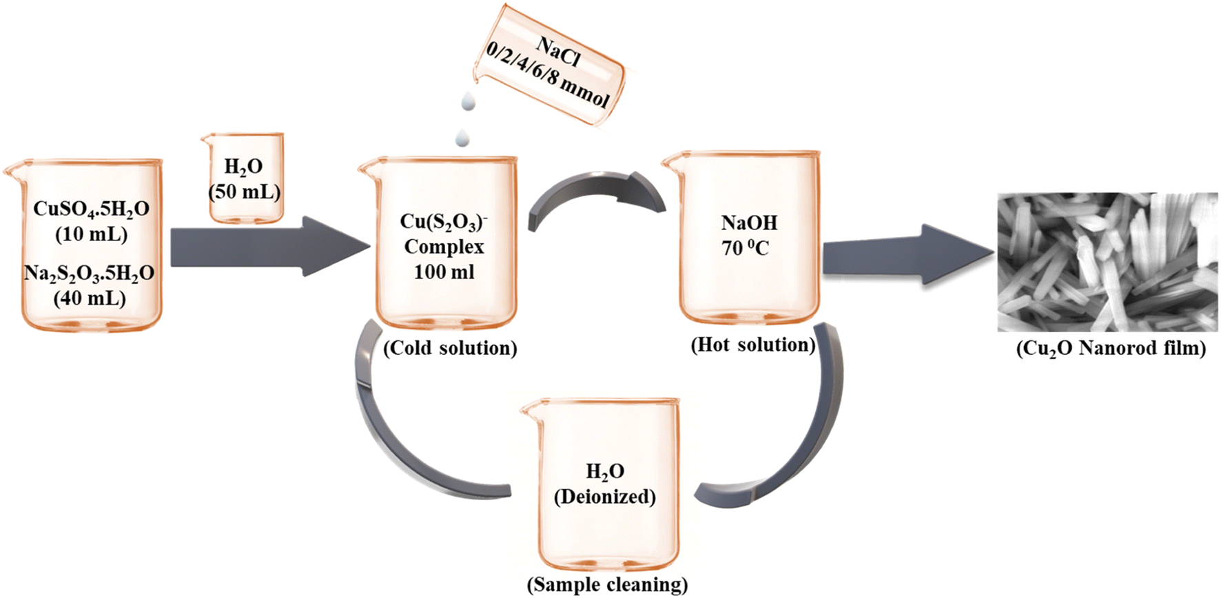
The above deposition process involved alternate immersion of the substrate into cationic and anionic precursor solution followed by rinsing in every immersion cycle to eliminate loosely adhered particles.36 Fig. 3 represents the synthesis of copper(I) oxide nanorod thin films in presence of NaCl using the SILAR deposition system.93 Earlier to the film deposition, the colorless copper–thiosulfate complex was made ready by mixing 10 mL 1 M copper(II) sulfate and 40 mL 1 M sodium thiosulfate into a 100 mL volumetric flask. Then, in addition to DI water, the required amount of NaCl electrolyte was further added to the same flask and the produced complex solution was the cold solution. Meanwhile, 2 M NaOH solution was kept constant at 70 °C and treated as the hot solution. The substrate such as soda lime glass was then alternatively submerged in cold and hot solutions respectively for the required time interval and completed one SILAR cycle. To fabricate a thin film, this procedure was repeated for up to several immersion cycles.
 |
| | Fig. 3 Synthesis of the copper(I) oxide nanorod thin films.93 | |
The formation of Cu2O nanorod thin films in presence of a NaCl electrolyte at various concentrations were discussed by using SEM micrographs as shown in Fig. 4. The film fabricated with no NaCl electrolyte demonstrated pencil-thin, and crack-free nanorod with an overgrown cluster in some areas on the substrate surface, as also detected in our earlier study.37 When 2 mmol of NaCl of the electrolyte was introduced into the solution, the crowded nanorods were developed, and the formation of nanorods enhanced with the increase in the concentration of NaCl to 4 mmol, showing a larger size and shape as observed in the Fig. 4(c). Very rough, tiny and dense spherical grains as well as some overgrown clusters were seen with an additional increase in the concentration of NaCl to 6 mmol. Such an overgrown cluster was produced due to the coalescence of the particles.94 Characteristically distributed, clear, and larger-sized spherical grains were revealed with further addition of NaCl electrolyte of 8 mmol. Thus, the NaCl electrolyte has the potential impact to change the surface morphologies from nanorods to spherical grains. The growth of Cu2O nanorod thin films was sensitive to the concentration of salts added as also stated for CuO.95 The growth of Cu2O nanostructures was increased gradually with the rise of NaCl concentration but until a limit. Such phenomena signify that NaCl concentration will consequence in similar morphology of the product and perform key roles in governing the size and shape of the Cu2O nanorods. Moreover, the steric hindrance caused by salt concentration might have affected the micelle aggregates, and these effects collected the assemblies of the products. More investigations are ongoing to elucidate the mechanisms for the growth process caused by the novel anticipated route.
 |
| | Fig. 4 SEM images of the samples fabricated at (a) 0 mmol, (b) 2 mmol, (c) 4 mmol, (d) 6 mmol, and (e) 8 mmol of NaCl electrolyte.93 | |
4. Factors affecting SILAR deposition process
4.1 Types of copper salts
In the SILAR technique, CuxO thin films were studied and fabricated by using different copper salts as summarized in Table 5. Generally, most of the studies were done by using CuSO4·5H2O as a basic salt for the formation of Cu2O thin films, whereas CuCl2·2H2O was used for the formation of CuO thin films. The mechanism of both salts was discussed elsewhere in this article.
Table 5 Raw materials are used for the formation of CuxO thin films by the SILAR method
| Formation |
Cationic precursors |
Complexing agents |
Anionic precursors |
Ref. |
| Cu2O |
Cu(CH3COO)2·H2O |
Na2S2O3·5H2O |
NaOH |
96 |
| CuSO4·5H2O |
Na2S2O3·5H2O |
NaOH |
96 |
| Cu(NO3)2·3H2O |
Na2S2O3·5H2O |
NaOH |
96 |
| CuCl2·2H2O |
Na2S2O3·5H2O |
NaOH |
96 |
| CuCl2·2H2O |
NH3 |
H2O2 |
97 |
| CuO |
CuCl2·2H2O |
NH3 |
H2O |
98 |
| Cu(CH3COO)2·nH2O |
NH4CH3COO |
H2O |
99 |
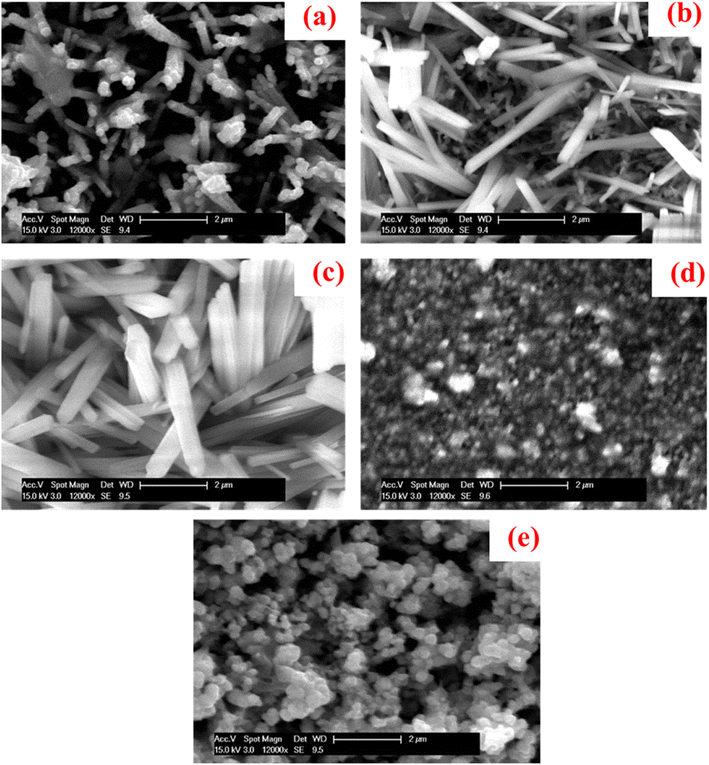
Altindemir et al. examined CuSO4·5H2O with the other three different salts such as (CH3COO)2·H2O, Cu(NO3)2·3H2O and CuCl2·2H2O to fabricate Cu2O thin films. Field emission-scanning electron microscope (FE-SEM) photographs of the deposited Cu2O thin films were demonstrated in Fig. 5(a)–(d). The deposited Cu2O thin film using the (CH3COO)2Cu·H2O salt demonstrated the cauliflower-like pattern having zero voids between the grains as seen from the images whereas, in the case of the CuSO4·5H2O salt, the grain size of the film showed the spherical form having no voids between the grains as in Fig. 5(a) and (b). The grain of the Cu2O thin film deposited using the Cu(NO3)2·3H2O salt revealed both cauliflower-like and rod shapes as in Fig. 5(c) whereas by means of the CuCl2·2H2O salt showed the cauliflower-like shape with discrete spaces between the grains as in Fig. 5(d).
 |
| | Fig. 5 The FE-SEM images of Cu2O nanostructured thin films deposited from four different Cu salts96 (a) (CH3COO)2Cu·H2O, (b) CuSO4·5H2O, (c) Cu(NO3)2·3H2O, and (d) CuCl2·2H2O. | |
On the other hand, CuCl2·2H2O salt was employed to fabricate CuO thin films using NH3 as a complexing agent. But Chatterjee and co-workers utilized H2O2 as an oxidizing agent with CuCl2·2H2O and NH3 solution to fabricate Cu2O thin films instead of CuO thin films.95 Similarly, Cu(CH3COO)2 nH2O and NH4CH3COO solution could be the potential choice to fabricate CuO thin films.99
4.2 pH of the precursor solution
Impact of solution pH on the properties of CuxO nanostructured thin films deposited by SILAR was studied in the pH scale range from 2.35 to 12 as shown in Table 6. The study was accomplished by controlling the pH of cationic and anionic precursor solutions by adjusting the additional acid and/or bases such as H2SO4, CH3COOH, NaOH and NH4OH.
Table 6 Properties of CuxO thin films deposited by varying solution pH applying SILAR method
| pH |
Precursors |
To alter pH |
Phase formed |
Thickness (nm) |
Crystallite (nm) |
Band gap (eV) |
Resistivity × 103 (Ω cm) |
Ref. |
| Cationic |
Anionic |
| OP = optimized precursor (2 M NaOH). |
| 2.35 |
[Cu(S2O3)]− |
2 M NaOHa |
H2SO4 |
Cu2O |
340 |
17 |
2.05 |
0.21 |
36 |
| 3.45 |
2 M NaOHa |
CH3COOH |
729 |
21 |
2.10 |
0.18 |
| 4.50 |
2 M NaOH |
CH3COOH |
800 |
15–22 |
2.30 |
72 |
37 |
| 5.10 |
2 M NaOH |
CH3COOH |
1000 |
2.28 |
103 |
| 6.20 |
2 M NaOH |
CH3COOH |
1800 |
2.43 |
742 |
| 7.33 |
2 M NaOHa |
— |
1130 |
18 |
2.15 |
0.37 |
36 |
| 7.33 |
1 M NaOH |
— |
336 |
13 |
2.16 |
0.18 |
| 7.95 |
2 M NaOH |
— |
1477 |
15–22 |
2.42 |
21.9 |
37 |
| 9.0 |
[Cu(NH3)4]2+ |
H2O |
— |
CuO |
42 |
37.4 |
1.61 |
— |
105 |
| 9.5 |
H2O |
— |
67 |
22.4 |
1.49 |
— |
| 10.0 |
H2O |
— |
85 |
22.9 |
1.49 |
— |
| 10.0 |
H2O |
H2SO4 |
520 |
14 |
2.17 |
6.5 |
94 |
| 10.5 |
H2O |
H2SO4 |
590 |
21 |
2.07 |
5.5 |
| 11.0 |
H2O |
H2SO4 |
680 |
27 |
2.02 |
4.0 |
| 11.5 |
H2O |
H2SO4 |
770 |
30 |
1.99 |
4.25 |
| 12.0 |
H2O |
H2SO4 |
820 |
36 |
1.89 |
4.5 |
To optimize the growth condition to fabricate the FTO/Cu2O/ZnO heterojunction solar cell, Farhad and co-workers extensively studied the effect of pH in between 2.35 and 7.95.36 During the study, the Cu2O thin films have grown by slightly modifying the original SILAR method,100 just by eliminating step 2 as shown in Chart 1 and named the technique as modified SILAR method. 10% H2SO4 and CH3COOH were added dropwise into cationic precursor solution to adjust solution pH, as well as the concentration of anionic precursor (NaOH), was also varied (1–2 M). The addition of CH3COOH into the optimized precursor solution (OP + CH3COOH) improved the quality of the crystal having a larger crystallite size of 21 nm whereas H2SO4 played the opposite role. Strong H2SO4 etches film thickness and it decreased with decreasing pH of the cationic precursor solution. From the SEM micrograph it is observed that the optimized solution (OP ∼ 2 M NaOH) showed compacted and larger spherical grains (D ∼ 231–259 nm) while the non-optimized solution (1 M NaOH) revealed irregular surface morphology with tiny grains (D ∼ 164 nm) which is as shown in Fig. 6. Grain size and band gap decreased with decreasing pH of cationic precursor solution such as 259–164 nm and 2.16–2.05 eV respectively. The electrical resistivity varies in the range of 0.18–0.38 kΩ cm and among optimized solutions OP + CH3COOH showed the lowest resistivity. The resistivity of the modified SILAR grown samples had (1–5) order magnitudes less than those deposited by Nair and Ristov's SILAR, and electrodeposition method.36
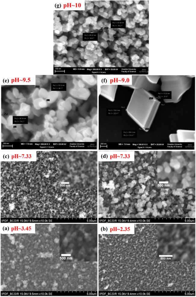 |
| | Fig. 6 SEM images representing {Cu2O: (a)–(d) and CuO: (e)–(g)} thin films deposited by varying pH.36,105 | |
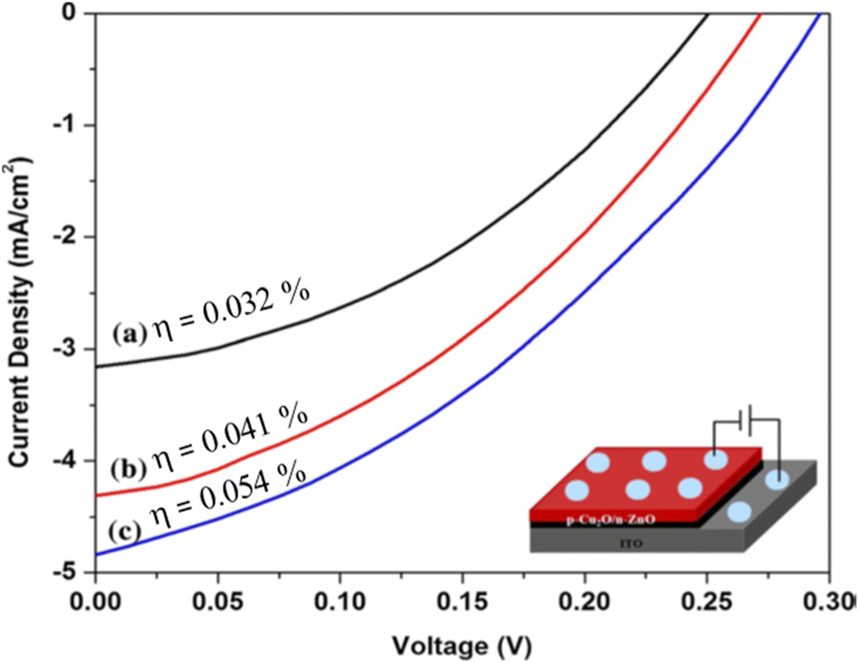
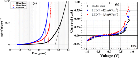
To justify further the effects of CH3COOH and rinsing steps, Farhad and co-workers again deposited thin films at pH 4.50–7.95 by adding CH3COOH into cationic precursor solutions.37,101 It is seen that film deposited without any rinsing step showed the lowest band gap due to the high film thickness and vice versa which is shown in Fig. 7(a). pH 5.10 which was maintained by adding CH3COOH exhibited a larger and densely packed grain size (∼300–530 nm) compared to pH 7.95 where no use of CH3COOH. Band gap and resistivity values were 2.41–2.30 eV and 742–72 kΩ cm respectively and decreased with decreasing pH of cationic precursor solution.37 The activation energy was 0.004–0.19 and 0.01–0.68 eV respectively in the temperature range 40–90 and 100–250 °C. In these studies, FTO/Cu2O/ZnO heterojunction shows diode-like characteristics101 at pH 7.95 as shown in Fig. 7(b) with maximum power (P) of ∼45 mW cm−2 under LED illumination with Knee voltage −0.5 V. These results indicate that CH3COOH has a significant influence on the controlling of the properties of Cu2O thin films.
 |
| | Fig. 7 (a) Variation of band gap with rinsing steps. (b) I–V characteristic curve for FTO/Cu2O/ZnO heterojunction cell grown on FTO substrate at pH-7.95.101 | |
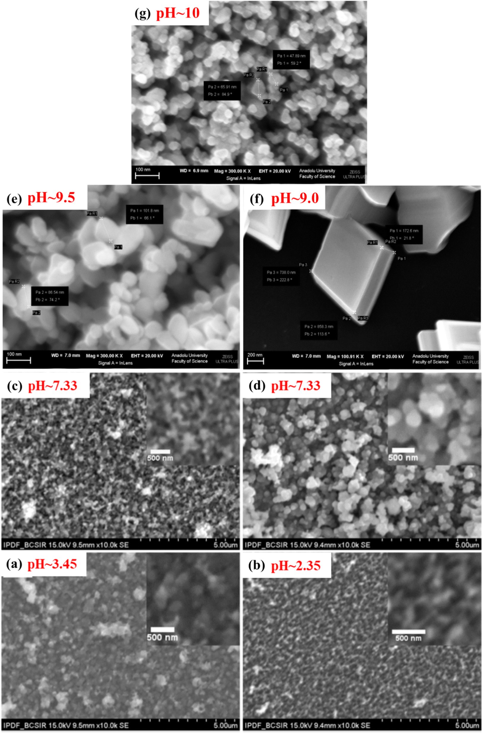
Umeri and coworkers described the effect of pH and growth temperature during the deposition of CuxO thin films94 at RT and 70 °C in the pH range from 8 to 11. At RT, the pure Cu2O phase exists with pH 8, while mixed phases of CuxO appeared at pH 11. Whereas, at 70 °C, only the pure Cu2O phase was deposited in the pH region of 8–11, which indicates that 70 °C is the optimum temperature for the growing phase of pure Cu2O thin films as also supported by other reported results.102 At 70 °C, the optical band gap (Eg) rises from 1.85 to 2.0 eV with the rise of pH from 8 to 11, while the trend showed the opposite at RT and declines from 2.0 to 1.6 eV with the rise of pH. This might be because of the change in the composition from Cu2O to CuO. From SEM micrographs, it is seen that at RT, the compact thin film was produced with pH 8 with an overgrown cluster in some spaces and when the pH increased to 11, overgrown cluster formation was diminished, and network-like nanofibers were observed. Conversely, at 70 °C and pH 9, a fiber-like nanostructure was formed, that looked like the morphology of films grown at RT with pH 11. Consequently, uniform, overgrown clusters free of close-packed and interconnected nanofibers of Cu2O were observed at 70 °C and pH 11 with a band gap of 2.0 eV. Thus, temperature-dependent pH has a significant controlling overgrowth and properties of the deposited films.
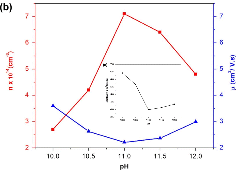
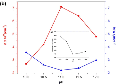
Likewise, Cu2O, the influence of pH on the physical properties of CuO thin films was investigated by Visalakshi et al.103 The pH (∼10–12) of the cationic precursor solution was maintained by adding concentrated NH4OH. Film thickness, crystallite size, and texture coefficient rise with the rising pH of cationic precursor solution but dislocation density and strain decreases. SEM images concluded that pH 10 and 10.5 exhibited cluster-like surface morphologies due to the coalescence of the grains but when it reached pH 11, uniformly distributed spherical grains were observed. At pH > 11 the agglomeration of the grains occurs which outcomes in larger grain size. The optical transmittance and band gap (2.17–1.89 eV) reduces with increasing pH. The resistivity decreases initially from 6.5 × 10³ to 4.0 ×10³ Ω cm with increasing pH from 10 to 11, then further increases with increasing pH. As represented in Fig. 8(a), with the increase of solution pH from 11 to 12, the carrier concentration decreases from 7.1 × 10¹⁴ to 4.8 × 1014 cm−3 which is in good agreement with the obtained result by Saravanakannan et al.104 Conversely, the mobility is first declined to pH 11; then, it is raised for further growth in pH. The decrease in mobility may be owing to the scattering formed at grain boundaries. The decrease in resistivity of the film synthesized at high pH may be attributable to the growth in film thickness without voids, whereas the rise in resistivity and decrease in carrier concentration and mobility detected at low pH may be owing to the existence of bulky voids. However, almost different properties were exhibited when the sample was annealed at 400 °C for 2 hours after deposition reported by Gençyılmaz and co-workers.105
 |
| | Fig. 8 (a) Electrical resistivity, (b) mobility and carrier concentration variation of SILAR-coated CuO thin films with pH.94,103 | |
4.3 Number of cycles during deposition
The film characteristic is closely related to the number of immersions of the substrates into the precursor solution. In almost all studies, the number of cycles is generally kept constant to understand the other properties of the CuxO films. There are few investigations where the effect of the number of cycles on the fabrication of CuxO films106–110 is discussed, as summarized in Table 7. It is obvious that with the increase of immersion cycles thickness of the films increase.
Table 7 Effect of the number of cycles on the fabrication of SILAR grown CuxO films
| Product |
Cycles |
Thickness (nm) |
Crystallite (nm) |
Dislocation density (δ × 10−3, nm−2) |
Strain (ε ×10−3) |
Bandgap (eV) |
Ref. |
| Cu2O |
50 |
550 |
16 |
3.72 |
6.82 |
2.11 |
106 |
| 75 |
830 |
19 |
2.90 |
6.01 |
2.06 |
| 100 |
1050 |
20 |
1.51 |
4.35 |
1.84 |
| 10 |
120 |
2.46 |
— |
— |
2.01 |
107 |
| 30 |
350 |
5.23 |
2.48 |
| 40 |
520 |
7.15 |
2.53 |
| 20 |
654 |
— |
— |
— |
2.48 |
37 |
| 40 |
1130 |
2.45 |
| 60 |
1200 |
2.41 |
| 80 |
1477 |
2.38 |
| CuO |
30 |
500 |
11 |
8 |
3.12 |
1.56 |
108 |
| 40 |
850 |
13 |
6 |
2.66 |
1.52 |
| 50 |
950 |
18 |
3 |
1.95 |
1.48 |
| 20 |
87 |
7 |
2.04 |
3.62 |
2.48 |
109 |
| 30 |
179 |
8 |
1.56 |
3.73 |
2.41 |
| 40 |
298 |
9 |
1.23 |
3.83 |
2.37 |
| 50 |
415 |
11 |
0.83 |
4.87 |
2.31 |
| 30 |
— |
10 |
10 |
3.43 |
1.92 |
110 |
| 40 |
15 |
4.44 |
2.27 |
1.89 |
| 50 |
24 |
1.74 |
1.42 |
1.69 |
The surface SEM morphologies of m-SILAR deposited Cu2O films in the top of the FTO substrates using 40, 60, and 80 immersion cycles were shown in Fig. 9(a)–(c). Throughout the area investigated, the surface morphology of all films was seen to be compact as well as coherently carpets. However, the Cu2O film grown with 40 immersion cycles demonstrated fiber-like microstructures with small grains of around 200 nm. Instead, thin films having 60 and 80 immersion cycles exhibited bigger spherically shaped grains of size around (200–550) and (350–650) nm respectively as shown in Fig. 9(b) and (c). This reflection recommends that grain size develops as the thickness increases with the increase of immersion cycles.37 As can be seen from Table 7 and Fig. 9(d), the optical bandgap of the Cu2O thin films deposited at pH ∼ 7.95 using 20 cycles (film thickness ∼ 654 nm), 40 cycles (film thickness ∼ 1130 nm), 60 cycles (film thickness ∼ 1200 nm) as well as 80 cycles (film thickness ∼ 1477 nm) were calculated to be ∼2.48, ∼2.45, ∼2.41 and ∼2.38 eV respectively. Obviously, there is a decreasing trend of optical bandgap with increasing film as represented in Fig. 9(d), probably due to the bigger grains usually existing in the thicker films, which verifies the results stated by Nair et al.111
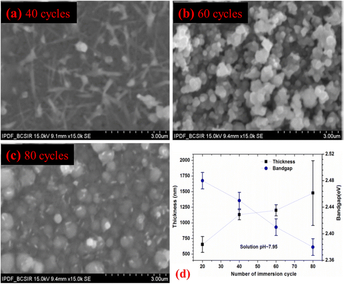 |
| | Fig. 9 SEM micrographs of the films grown with different immersion cycles at pH: 7.95 for (a) 40 cycles (b) 60 cycles (c) 80 cycles and (d) film thickness of Cu2O thin films using different immersion cycles grown by m-SILAR.37 | |
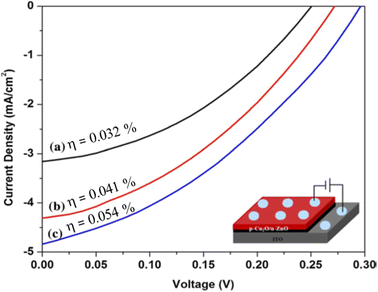
Fig. 10(a)–(c) demonstrates the Cu2O nanostructured films fabricated with different dipping cycles of the nanorods spread homogeneously on the substrate surface, showing a large number of grains with fine particle edges. As seen from morphological studies and Table 7, 50 cycles grown sample has a smaller crystallite size and higher dislocation density with good nanorod morphology. For light absorption, although it has an opportunity for a larger surface area to the photoelectrode, due to the presence of considerable grain boundaries, it creates recombination problems in the film. So, the electron trapping at the surface and in the intergrain boundaries lowered the efficiency value of the film grown through 50 cycles. The samples deposited by 75 and 100 cycles have comparatively better crystallite size and lower dislocation density, which leads to reduce grain boundaries.106 Due to the drop in grain boundary resistance, the photogenerated charge carriers can significantly reduce the recombination losses. The cell was fabricated as ITO/ZnO NRs/Cu2O/Al with varied efficiency mainly due to the number of cycles of the films shown in Fig. 11. Even though the attained efficiency of the ZnO/Cu2O heterojunction was lower, the efficiency was high in the samples deposited at high cycles such as 100. Hence, the effect of the film thickness on cell performance was evidenced by the enhancement of efficiency due to the substantial development of crystallinity and absorbance of Cu2O films.
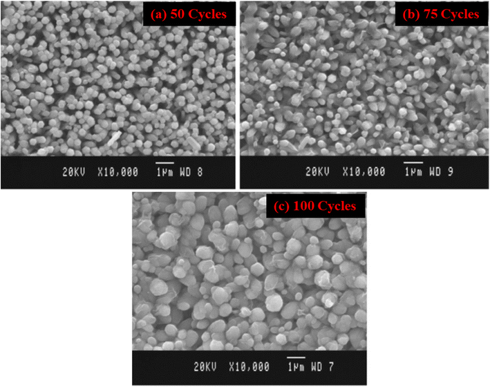 |
| | Fig. 10 SEM image of the Cu2O nanostructured films deposited at (a) 50 (b) 75 and (c) 100 dipping cycles.106 | |
 |
| | Fig. 11 Current–voltage curve of ITO/ZnO NRs/Cu2O/Al cells (a) 50 (b) 75 and (c) 100 dip Cu2O films.106 | |
4.4 Effect of bath temperature
Fig. 12(a) illustrates the deposition of the thin films grown by varying bath temperatures of anionic precursors as a function of the immersion cycles. The figure demonstrated that the fabrication rate reduced as the immersion cycle proceeds characteristically at 10 nm per cycle. In the case of fabrication using the alkali solution at 90 °C, the production was faster, and the film thickness was >0.3 μm with 20 cycles of immersions, whereas, at 70 °C, the film growth slightly falls after 20 immersions.111 For the films fabricated with NaOH solution temperature of 50–90 °C, the photo response curves were given for a range of thicknesses as demonstrated in Fig. 12(b). Irrespective of the solution temperature, the dark current and the photocurrent logged in the films were comparable for the films with thicknesses smaller than 0.1 mm. The values were higher in samples fabricated using NaOH solution at 70 °C having films of higher thickness. The measured electrical conductivity of a 0.15 μm film is about 5 × 10⁻⁴ Ω−1 cm−1. And it was found that the increase of film thickness of two orders increases the conductivity by nearly two orders.
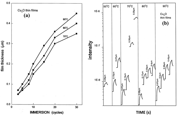 |
| | Fig. 12 Samples in NaOH solution (a) at different temperatures as a function of film thickness and immersions. (b) At the designated temperatures to record the photocurrent response of the Cu2O thin films of different thicknesses.111 [Light source: tungsten–halogen, intensity of illumination: 1 kW m−2, time length: 60–180 s, bias: 1 V applied across Ag print electrodes 5 mm (long) × 5 mm (separation)]. | |
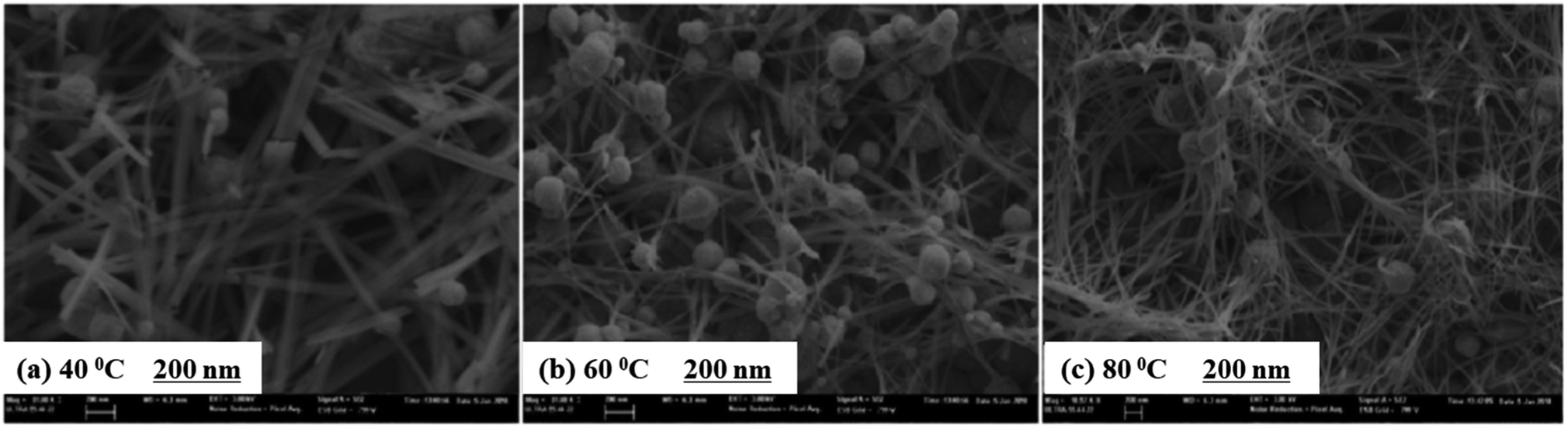
The structural parameters, elemental composition, and optical band gap for different bath temperature of Cu2O films are given in Table 8, studied by Baig et al.112 It is seen from the table that when the temperature climbed from 40 to 80 °C, the size of grain increased from 16.78 to 18.84 nm whereas strain in the crystal lattice was reduced. The fall in strain signifies that the imperfection in the crystal lattice with the rising temperature was decreased. The SEM images of Cu2O thin films deposited on ITO substrate with different anionic bath temperatures are demonstrated in Fig. 13. From the figures, with the rise of anionic bath temperature the structure of the wire became compact compared to that at 40 °C. Likewise, the oxygen concentration was decreased with an increase in temperature as observed in Energy-dispersive X-ray spectroscopy (EDS) value of Cu2O film in Table 8. Further, the photocatalytic activity for water splitting by the deposited Cu2O thin films at different temperatures was studied in a photochemical cell and the result revealed that film grown at 80 °C had a higher current ratio with respect to the other two samples and the photocurrent produced by that sample is relatively steady (figure in 5.2 section).
Table 8 Structural parameters, elemental composition (EDS), and optical band gap for different bath temperatures of Cu2O films
| Bath temperature (°C) |
D (nm) |
Dislocation density (δ) × 1014 m−2 |
Micro strain (ε) |
Atomic (%) |
Band gap (eV) |
| Cu |
O |
| 40 |
16.78 |
35.51 |
0.007025 |
50.75 |
49.25 |
2.25 |
| 60 |
17.10 |
34.19 |
0.006892 |
56.45 |
43.55 |
2.14 |
| 80 |
18.84 |
28.17 |
0.006193 |
61.76 |
38.24 |
2.07 |
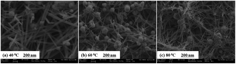 |
| | Fig. 13 SEM images of Cu2O nanostructured thin films deposited by SILAR at different bath temperatures (a) 40 °C, (b) 60 °C, and (c) 80 °C.112 | |
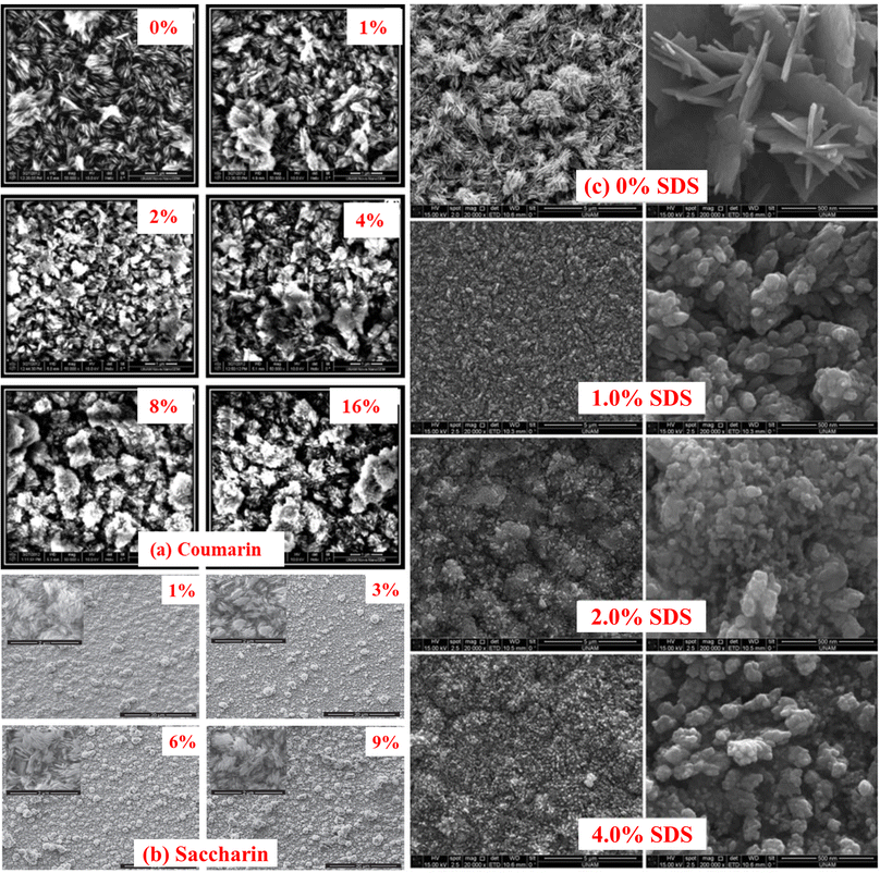
4.5 Addition of additives
The influence of the different additives on the surface morphological characteristics of CuO films was studied by using SEM. Fig. 14 illustrates the SEM images of the CuO thin films fabricated in the solution containing additives such as coumarin, saccharin, and sodium dodecyl sulfate (SDS) having different concentrations. In the first step without coumarin, Fig. 14(a) there were plate-like CuO nanostructures that homogenously cover the entire surface. Then, the nanostructures start to change their shapes with the increase of coumarin concentration, form some clusters on the surface and lose their homogeneity. From Fig. 14(b), in the case of saccharin, it was observed that all the samples have nearly the same morphology that is they are all composed of plate-like nanostructures as in ref. 113. On the other hand, the homogeneity of the films deteriorates with increasing saccharin concentration. In the case of SDS, Fig. 14(c) demonstrates that the fabricated CuO thin films were adhered and spread well onto the substrate surface without SDS. With the addition of SDS and its concentration, the surface morphology of the CuO film was changed dramatically. From this viewpoint, the discrepancy of SDS molar concentration impressed the morphology of the surface of all the fabricated thin films. This variation in morphology may be owing to the electrostatic interaction between Cu2+ and CH3(CH2)11OSO3−. SDS may affect particle growth as well as morphology after nucleation. Thus, during the crystallization process, the SDS can affect nucleation.114
 |
| | Fig. 14 SEM images of CuO nanostructured thin films as a function of different additive concentrations, such as (a) coumarin,115 (b) saccharin116 and (c) SDS.117 | |
Through UV-Vis's spectrophotometer study, it was clear that both the optical band gap and the transmission spectra were affected by the additive concentration. The band gap, as well as spectral transmittance values of the films, were decreased for the higher content of both coumarin and saccharin,115,116 while showing the opposite tendencies in the case of SDS. The optical bandgap energy of both organic (coumarin and saccharin) additives decreased from around 1.50 to 1.27 eV, while increased from 1.32 to 1.49 eV for inorganic SDS, with the increasing concentration of the additives.117
4.6 Complexing agent
Cavusoglu and co-workers studied the role of the complexing agent such as triethanolamine (TEA) mediated fabrication of nanocrystalline CuO thin films via SILAR technique at room temperature and the results are summarized in Table 9. As a function of increasing TEA concentration, the optical band gap energy of the fabricated CuO thin films was increased from 1.33 to 2.00 eV while the average transmittance of all the films increased from 2.5 to 42.5%. A minimum resistivity of 3.74 × 10⁵ Ω cm was found with zero TEA in CuO thin films whereas, with a TEA concentration of 1.0 M%, the resistivity subsequently increased to 509 × 105 Ω cm. Surface morphology on the film surfaces demonstrated the homogeneous distribution of the nanostructured CuO as demonstrated in Fig. 15(a)–(d) whereas, the figure of merit (FOM) was represented as a function of TEA concentration as shown in Fig. 15(e). TEA concentration of 0.25 M% in CuO thin film provided the high FOM values of 786 × 10−12 Ω−1 at distinct wavelengths of between 600 and 900 nm.118 Therefore, the range of optical and electrical properties developed by such a study having a different complexing agent is favorable for the applications of numerous optoelectronic devices.
Table 9 Properties of CuO thin films as a function of TEA concentrations
| TEA concentration M% |
Crystallite (nm) |
Thickness (nm) |
Bandgap (eV) |
Conductivity (σ) ×10−6 (Ω cm)−1 |
Resistivity (ρ) ×105 Ω cm |
FOM × 10−12 Ω−1 |
| 0 |
19.95 |
797 |
1.33 |
2.67 |
3.74 |
149 |
| 0.25 |
19.80 |
387 |
1.57 |
1.05 |
9.50 |
786 |
| 0.50 |
18.92 |
199 |
1.67 |
0.07 |
149 |
37.2 |
| 1.00 |
17.47 |
101 |
2.00 |
0.02 |
509 |
1.70 |
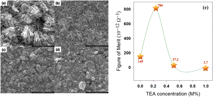 |
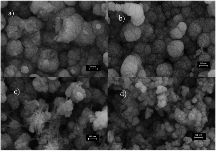
| | Fig. 15 SEM images of CuO thin films at (a) 0 M%, (b) 0.25 M%, (c) 0.50 M%, (d) 1.00 M% as well as (e) FOM with TEA at different molar concentrations.118 | |
4.7 Annealing of as-deposited films
Annealing is a vital parameter to control the phases of the deposited thin films. Both the phases of CuxO could be synthesized by changing the atmospheric condition (air, vacuum) and temperature of annealing as summarized in Table 10. Here, air or oxygen37,101,119–124 annealing of the SILAR-grown films has been studied more extensively than vacuum annealing.125 Recently, SILAR deposited CuxO films are mainly studied between 75 to 500 °C37,101,119–124 in presence of air or N2. The study revealed that Cu2O phase was stable until 250 °C,120,122 though Farhad and co-workers showed a mixed phase of both Cu2O and CuO at 250 °C37 due to the pH effect, while Ozaslan et al. showed a mixed phase even at 500 °C.123 The CuO phase could be found at 300 °C120 by annealing of Cu2O or even could be deposited by using NH3 solution (pH = 10) with the reaction of CuCl2 at ambient temperature.124
Table 10 Annealing of the SILAR grown CuxO nanostructured thin films
| Anionic salt, NaOH (M) |
Cycles |
Time |
Temperature |
Crystal phase |
Crystallite (nm) |
Band gap (eV) |
Ref. |
| Dipping (s) |
Annealing (min) |
Growth (°C) |
Annealing (°C) |
| CuSO4·5H2O + NaOH + Na2S2O3·5H2O |
| 0.5 |
20 |
20 |
— |
70 |
200–400 |
As deposited: Cu2O |
27.76 |
— |
119 |
| 200 °C: Cu2O |
49.95 |
| 300 °C: Cu2O + CuO |
40.88 |
| 400 °C: CuO |
62.32 |
| 1 |
10 |
20 |
60 |
70 |
200–350 |
As deposited: Cu2O |
14 |
2.20 |
120 |
| 200 °C: Cu2O |
14 |
2.20 |
| 250 °C: Cu2O |
14 |
2.20 |
| 300 °C: CuO |
14–26 |
1.35 |
| 350 °C: CuO |
— |
1.35 |
| 1 |
30 |
20 |
— |
70 |
200–400 |
As deposited: Cu2O |
14–26 |
2.40 |
121 |
| 200 °C: Cu2O |
2.40 |
| 300 °C: Cu2O + CuO |
2.06 |
| 400 °C: CuO |
1.73 |
| 1 |
30 |
20 |
— |
50–90 |
250–400 (air, N2) |
As deposited: Cu2O |
∼18 |
2.10 |
122 |
| 250 °C: Cu2O |
2.10 |
| 300 °C: Cu2O + CuO |
— |
| 350 °C: CuO |
1.75 |
| 400 °C: CuO |
1.75 |
| 2 |
40 |
2 |
60 |
70 |
100–500 |
As deposited: Cu2O |
— |
2.57 |
123 |
| 100 °C: Cu2O |
2.52 |
| 300 °C: Cu2O (2.27%) + CuO (97.73%) |
2.45 |
| 500 °C: Cu2O (1%) + CuO (99%) |
1.91 |
| 2 |
40–80 |
— |
60–180 |
70 |
75–350 |
As deposited: Cu2O |
15–22 |
2.42 |
37 |
| 75 °C: Cu2O |
2.02 |
| 150 °C: Cu2O |
1.98 |
| 200 °C: Cu2O |
1.94 |
| 250 °C: Cu2O + CuO |
1.62 |
| 350 °C: Cu2O + CuO (1 h) |
— |
| 350 °C: CuO (3 h) |
1.44 |
| 2 |
60 |
5 |
60 |
70 |
350 |
As deposited: Cu2O |
|
2.06–2.16 |
101 |
| 350 °C: Cu2O + CuO (1 h) |
1.43–1.51 |
|
| CuCl2 + NH3OH + H2O2 |
| — |
2–10 |
30 |
30 |
RT |
20–500 |
As deposited: Cu2O |
14 |
2.17 |
124 |
| 100 °C: Cu2O |
14 |
2.22 |
| 150 °C: Cu2O |
14 |
2.17 |
| 450 °C: CuO |
16 |
1.43 |
| 500 °C: CuO |
16 |
1.44 |
| — |
400 |
>30 |
60 |
RT |
27–600 (air, vacuum) |
As deposited: Cu2O |
14–21 |
2.30 |
125 |
| 100 °C: Cu2O |
2.40 |
| 400 °C: CuO |
1.85 |
| 600 °C: CuO |
1.70 |
|
| CuCl2 + NH3 solution (pH = 10) |
| — |
80 |
30 |
30 |
— |
200–400 |
As deposited: CuO |
11.09 |
1.17 |
126 |
| 200 °C: CuO |
12.05 |
1.29 |
| 300 °C: CuO |
13.86 |
1.30 |
| 400 °C: CuO |
14.88 |
1.36 |
Amudhavalli and co-workers successfully showed the increasing trend of the crystallite size of copper oxides with the increase of annealing temperature while depositing the films at 0.5 M NaOH. Fig. 16 demonstrated the change of resistivity, mobility, and carrier concentration of copper oxide (Cu2O and CuO) phases with annealing temperature as shown by Ozaslan et al.123 It is found that the carrier concentration was decreased from 3.07 × 10¹⁷ to 6.61 × 1015 cm−3 with increasing annealing temperature from 70 to 500 °C respectively. The hole mobility of the films was increased from 4.20 to 31.87 cm2 V−1 s−1 with decreasing the carrier concentration, while the electrical resistivity of the films decreased with annealing temperature, inducing the increment in the conductivity of the films. Nair et al. observed the dark conductivity of the CuO film produced by air annealing of a 0.15 μm Cu2O film at 400 °C is high about 7.2 × 10⁻³ Ω−1 cm−1.
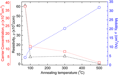 |
| | Fig. 16 Representation of the change of resistivity, mobility, and carrier concentration of copper oxide (Cu2O and CuO) films with annealing temperature.123 | |
4.8 Doping by diverse dopants
Tuning of the structural, electrical, and optical properties of SILAR-deposited CuxO films through Fe, Eu, Zn, Co, B, Mg, Ni, and Pb doping has been reported extensively by several authors. The summary of the effect of doping on SILAR-deposited CuxO films is represented in Table 11. Interestingly, in the case of Cu2O film fabrication, the reactants were the same except for the doping materials such as Fe, Eu, Zn, and Co.127–130 Similarly, during Co, B, Mg, and Pb doping into CuO films,131–134 the reactants were also the same except in the case of Ni doping.135
Table 11 CuxO nanostructured materials grown in presence of different dopants with their properties
| Product |
Dopant |
Cycle |
Crystallite (nm) |
Grain (nm) |
Bandgap (eV) |
Ref. |
| Material |
Amount |
| Reactants: CuSO4·5H2O + NaOH + Na2S2O3·5H2O |
| Fe: Cu2O |
FeSO4 (wt%) |
0 |
30 |
62.83 |
— |
1.80 |
128 |
| 1 |
59.80 |
2.10 |
| 2 |
41.83 |
2.36 |
| 5 |
36.40 |
2.45 |
| Eu: Cu2O |
Eu(NO3)3·5H2O (at%) |
1 |
100 |
27 |
— |
2.08 |
129 |
| 3 |
24 |
2.26 |
| 5 |
21 |
2.41 |
| Zn: Cu2O |
ZnSO4 (wt%) |
0 |
50 |
18 |
— |
2.34 |
130 |
| 1 |
30 |
2.35 |
| 2 |
39 |
2.37 |
| 3 |
52 |
2.38 |
| 5 |
69 |
2.41 |
| 10 |
44 |
2.39 |
| Co: Cu2O |
CoSO4 (wt%) |
0 |
30 |
62.83 |
— |
1.94 |
127 |
| 1 |
53.30 |
2.03 |
| 2 |
48.47 |
2.12 |
| 5 |
39.24 |
2.18 |
| 10 |
28.44 |
2.47 |
|
| Reactants: CuCl2·2H2O + H2O + NH3 |
| Co: CuO |
CoCl2·6H2O (at%) |
0 |
10 |
22.7 |
70 |
1.53 |
132 |
| 0.5 |
15.7 |
44 |
1.47 |
| 1 |
13.6 |
42 |
1.45 |
| 2 |
13.1 |
36 |
1.41 |
| 3 |
12.6 |
32 |
1.38 |
| 4 |
12.2 |
38 |
1.36 |
| B: CuO |
H3BO4 (at%) |
0 |
10 |
12.9 |
45 |
1.52 |
131 |
| 1 |
13.1 |
42 |
1.48 |
| 2 |
14.2 |
38 |
1.43 |
| 3 |
15.9 |
30 |
1.39 |
| Mn: CuO |
Mn(NO3)2 (at%) |
0 |
10 |
— |
9.94 |
1.42 |
133 |
| 1 |
7.83 |
1.98 |
| 3 |
8.21 |
2.08 |
| 5 |
9.76 |
2.20 |
| Pb: CuO |
Pb(NO3)2 (at%) |
0 |
10 |
— |
9.94 |
1.43 |
135 |
| 1 |
17.22 |
1.80 |
| 2 |
16.21 |
1.76 |
| 4 |
15.79 |
1.72 |
| 8 |
13.07 |
1.68 |
| 16 |
8.98 |
1.65 |
|
| Reactants: Cu(CH3COO)2·nH2O + H2O + NH4CH3COO |
| Ni: CuO |
Ni(CH3COO)2·nH2O |
|
30 |
— |
10–15 |
— |
134 |
In the case of Co or Fe doping, the crystallite size of the films of Cu2O decreased between 62.83 and 28.44 nm when the concentration of the doped material increased gradually, whereas it showed an opposite trend in the case of Zn doping. Interestingly, Fe, Eu, Zn and Co doping into Cu2O rises the bandgap of the material a little in every case. On the other hand, in the case of Co and B doping into CuO films, the bandgap deceased while it was increased for Mg and Pb doping.
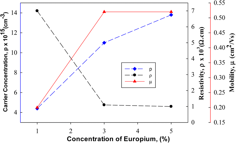
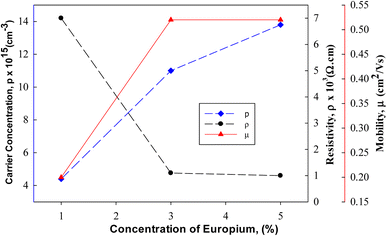
The films prepared at high doped Cu2O thin films such as 5% Eu showed a low resistivity value of 1 × 10³ Ω cm as shown in Fig. 17. The Hall mobility and carrier concentration values in such cases are 0.52 cm2 V−1 s−1 and 13.8 × 1015 cm−3, respectively.
 |
| | Fig. 17 Resistivity, carrier concentration and mobility for Eu doped Cu2O films.129 | |
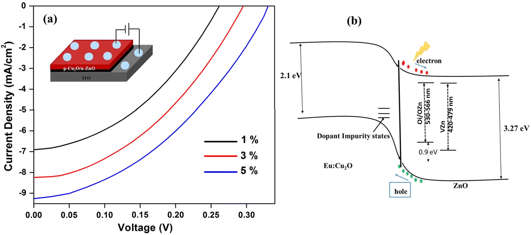
Fig. 18(a) shows the current density–voltage (J–V) characteristics of the ZnO/Cu2O heterojunction solar cells prepared using the Eu-doped Cu2O thin films. The Voc was increased with increasing Eu content from 265 mV (1% Eu) up to 332 mV (5% Eu). The conversion efficiency can be enhanced by dropping recombination centers avoiding lattice-mismatch defects, and by reducing the resistance of Cu2O. The ionic radius of Eu3+ ion was 0.109 nm whereas, Cu+ is 0.077 nm. Therefore, Eu3+ ion could not be incorporated by substitution rather it was incorporated as an interstitial creating getter center. It overwhelms the recombination losses and thus advances current levels and improved Eu doping levels.136
 |
| | Fig. 18 (a) 1%, 3% and 5% Eu doped thin films having current–voltage characteristics of ITO/ZnO NRs/Eu: Cu2O/Al cell, (b) carrier transport and band structure of p–n junction.129 | |
Fig. 18(b) illustrates the band structure as well as carrier transport of the deposited p–n junction. As there was much difference between conduction and valence band off-sets triggering effective separation of charge carriers, a built-in potential barrier was developed. When the light was absorbed onto the device photocarriers were generated and drifted to the respective electrodes depending upon the applied potential causing current conduction. As an acceptor dopant, impurity levels of Eu were adjacent to the valence band edge. In the case of ZnO, the green luminescence at 535 nm could be produced by the diffused Cu ion and replacing Zn. The VO center was atop the valence band whereas the Zn vacancy was (VZn) in an acceptor level, which occurred at 0.8 eV. Nevertheless, the ZnO coated over Eu: Cu2O performed as a passivation layer improving the Voc and declining the consequence of impurity center-mediated recombination loss.137,138
Magnetic measurements were performed by employing a vibration sample magnetometer (VSM) at ambient temperature for both Fe and Co-doped Cu2O. Undoped Cu2O has a diamagnetic property.139 The outcome agrees with Fig. 19(a) and (b) which demonstrate the change of magnetization against the applied magnetic field (M–H). In the case of Co-doped Cu2O, undoped and minimum doped such as 1 and 2 wt% films showed diamagnetic (high magnetization) behavior whereas, at the maximum doped such as 10 wt%, the films showed ferromagnetic (low magnetization) properties.140 The diamagnetic order was Cu2−xCoxO (x = 0 > 1 > 2 > 5 > 10 wt%). The ferromagnetic behavior was possibly due to the intrinsic coupling (Co–Co) between the atoms of doped material. Similarly, in the case of 1% Fe doped Cu2O at 305 K, the film showed diamagnetic properties. An increase of the Fe-doping (2 wt%), slightly altered the diamagnetic property because of the increased hole concentrations and further doping of Fe ions (5 wt%), the film showed anti-ferromagnetic behavior. With the increase in the concentration of Fe, both the number of Fe3+–Cu2+ pairs and the hole concentrations increased and consequently, the crystallite size reduced.
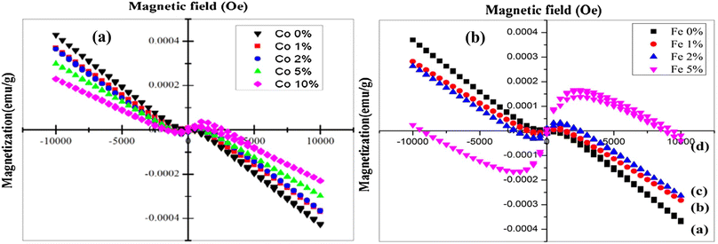 |
| | Fig. 19 Magnetic behavior of (a) Co-doped127 (b) Fe-doped Cu2O thin films.128 | |
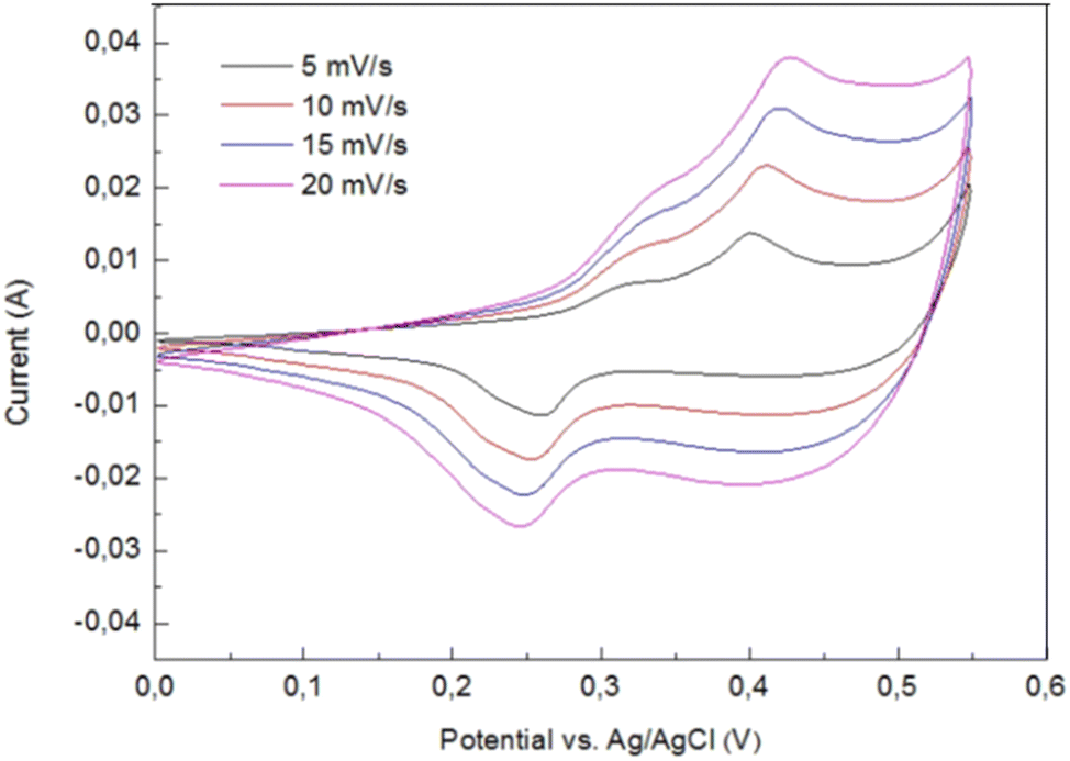
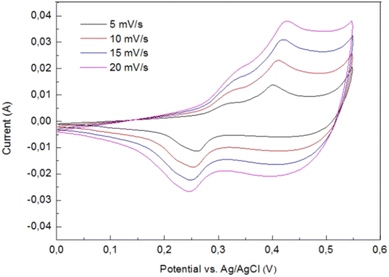
Lobinsky and co-workers studied the cyclic voltammograms of the nickel foam electrode with Ni-doped CuO nanolayers in a potential space between 0 and 550 mV vs. Ag/AgCl electrode at the scanning rates of 5, 10, 15 and 20 mV s−1 as shown in Fig. 20. Two of the redox reactions on the anodic curve took place in the layer, including the Cu+ → Cu2+ transformation at 310 mV while the Ni2+ → Ni3+ at 390 mV at a scan rate of 5 mV s−1. The proportionality of currents to scan rate delivers data that the film is sufficiently thick, and the charge transfer rate was restricted by the diffusion of charge carriers in the film.134
 |
| | Fig. 20 CVA curves for nickel foam electrode with Ni-doped CuO nanolayers at a scan rate of 5, 10, 15 and 20 mV s−1.135 | |
Inset of Fig. 21 demonstrates the specific capacitance of the Ni-doped CuO nickel foam electrode, which was found from charge–discharge curves, and it was 154 mA h g−1 (1240 F g−1) at the current densities of 1 A g−1.135 The high value of the specific capacitance of the sample can be explained based on the good conductivity of CuO and the substantial role of Ni atoms in pseudo-capacity. The capacity retention of the Ni foam electrode with Ni-doped CuO nanolayers after 1000 charge–discharge cycles at a current density of 2 A g−1 was retained at 92%, showing good cycling stability of the material as presented in Fig. 21. High cycling stability could be described by the feature morphology of ultrathin nanocrystals of CuO which deliver fast diffusion of ions on the electrode surface and while not being ruined in the charge–discharge process.
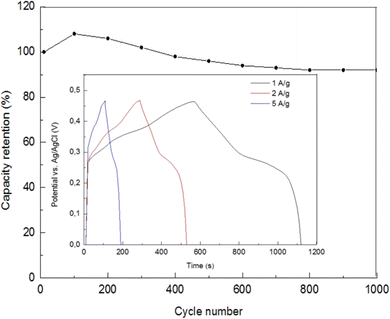 |
| | Fig. 21 The cycling stability for the Ni Foam electrode with Ni-doped CuO nanolayers at 2 A g−1 whereas the inset graph represents galvanostatic charge–discharge curves of the electrode with Ni-doped CuO nanolayers.135 | |
5. Applications
The optoelectronic properties of SILAR synthesized thin films have shown outstanding performance in diverse applications, for instance, photovoltaics,141 supercapacitors,142,143 photoelectrochemical water splitting,144 gas sensors143,145 and many more. The method appears to be easier and represents an efficient way to manufacture devices. Some of the potential applications such as antibacterial activities, supercapacitors, surface wettability and photoelectrochemical water splitting in presence of CuxO nanostructured thin films will be discussed in the following section.
5.1. Antibacterial activities
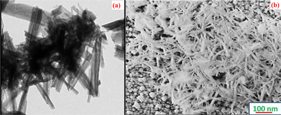
To control pathogens, nanoparticles are in great demand due to their huge applications in the health industries. Results achieved from nanocrystalline Cu2O nano-thin films fabricated by Dhanabalan et al. possessed substantial antimicrobial activity against the experienced human pathogen at a maximum inhibition zone of 16 mm against Gram-positive Staphylococcus aureus.146 The surface morphological studies exhibited that the needle-shaped grains which play a crucial role in the antibacterial activity of the fabricated Cu2O films by SILAR technique as shown in Fig. 22(a) and (b). The synthesized Cu2O thin film can exhibit antibacterial activity from 18 to 24 hours of incubation time. The bacterial growth will decrease with the increase in the concentrations of nanoparticles, which may be the cause of the reduction of voids affording space for the growth of bacteria that remains resistant to the pathogenic bacterial strain.
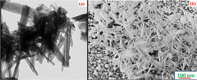 |
| | Fig. 22 (a) TEM (b) SEM images of the Cu2O grains showing needle-shaped uniformity on the surface.146 | |
5.2. Water splitting
CuxO was considered a good candidate for photoelectrochemical (PEC) water splitting due to its abundance, low price, and high stability in aqueous solution.147,148 Baig et al. fabricated Cu2O at a high bath temperature of 80 °C by SILAR which showed high photocurrent and good stability111 as discussed earlier. The photocatalytic activity for water splitting of the Cu2O thin film was studied with the photochemical system containing Pt (counter), Ag/AgCl (reference), Cu2O (working electrode) and KCl (pH = 13.6) as electrolytes. PCE data shown in Fig. 23 revealed that samples synthesized at 80 °C have a higher current ratio and produced a stable photocurrent compared to the other samples by using a 300 W Xenon lamp (PLSSXE300/300UV).
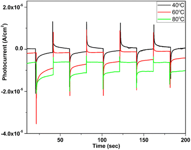 |
| | Fig. 23 PEC measurement of Cu2O thin films at different bath temperatures.111 | |
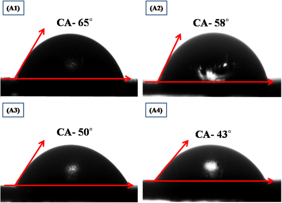
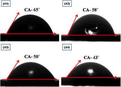
5.3. Surface wettability study
The surface wettability study of films determines its capability to interact with ions when immersed into electrolyte by measuring the contact angle with liquid electrolyte as shown in Fig. 24.149 If the contact angle is >90°, then the film surface is hydrophobic, while for <90°, it is hydrophilic. For better interaction of electrolyte ions, the contact angle must be as low as possible with the electroactive site on the thin film surface.150,151 Fig. 24 (A1, A2, A3, and A4) signifies the image of the contact angle with the surface of the film. The observed angles of CuO thin films with 50, 60, 70 and 80 SILAR cycles were 65°, 58°, 50°, and 43°, respectively. The observed CuO films were hydrophilic in nature, as the contact angles for CuO decline with the rise in SILAR cycles, which will allow more interaction of electroactive sites of the CuO on the film surface.
 |
| | Fig. 24 Study of surface wettability of CuO thin films,149 (A1) 50 SILAR cycles, (A2) 60 SILAR cycles, (A3) 70 SILAR cycles and (A4) 80 SILAR cycles. | |
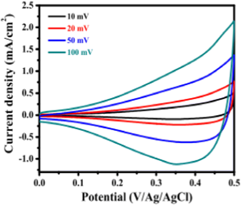
5.4. Super capacitive behavior
The electrochemical impedance, as well as super capacitive properties, of SILAR synthesized CuO thin films are studied by Patil et al.149 The synthesized CuO thin film showed the lowest charge transfer resistance of 41.45 Ω cm−2 with the highest specific capacitance of 184 F g−1 at the scan rate of 50 mV s−1 and demonstrated 83% capacitive retention after 5000 cycles. Super capacitive performance of the film was verified using cyclic voltammetry (CV) in 1 M KOH electrolytes in a three-electrode cell equipped with CuO (working electrode), Pt (counter electrode) and saturated Ag/AgCl (reference electrode). As shown in Fig. 25, the CVs were studied with a potential window of 0 to 0.6 V/Ag/AgCl at several scan rates such as 10, 20, 50 and 100 mV s−1.
 |
| | Fig. 25 Cyclic voltagramms of CuO with various scan rates of 1 M KOH electrolyte.149 | |
To examine the charge–discharge properties of CuO, the chronoamperometry technique was applied. Fig. 26(a) demonstrates galvanostatic charge–discharge curves at various current densities for CuO and signify a good capacitive behavior of CuO electrode as ref. 152. In Fig. 26(b), the difference of specific capacitance with various scan rates was displayed, which enhanced exponentially with decreasing scan rate.153 The electrochemical stability of CuO film electrode was examined by applying CVs at a scan rate of 100 mV s−1 for 5000 cycles. Fig. 26(c) demonstrated the cyclic voltammetry scan of CuO film electrode after the 1st to 5000th cycles and confirmed cyclic stability of 83% after 5000 cycles. By using the Ragone plot, the highest values of specific power and specific energy were measured as 3 and 14.1 W h kg−1, respectively, using the GCD technique at a current density of 1 mA cm−2 for CuO electrode attained in the potential range from 0 to 0.5 V as shown in Fig. 26(d).
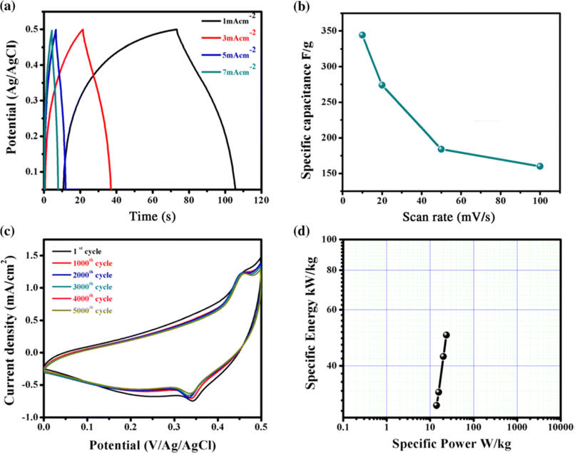 |
| | Fig. 26 (a) Representation of galvanostatic charge–discharge curves of CuO at diverse current densities. (b) Change of specific capacitance with scan rate (c) study of stability of CuO thin films (d) specific energy versus specific power of Ragone plot.149 | |
Moreover, the electrochemical investigation of Ni-doped CuO nanolayers modified with Ni foam electrodes synthesized by Lobinsky et al. revealed the specific capacitance of 154 mA h g−1 (1240 F g−1) at a current density of 1 A g−1,135 as already discussed in the doping section. Thus, SILAR-grown CuO material can be potential usage as an electroactive resource for alkaline batteries and pseudo-capacitors.
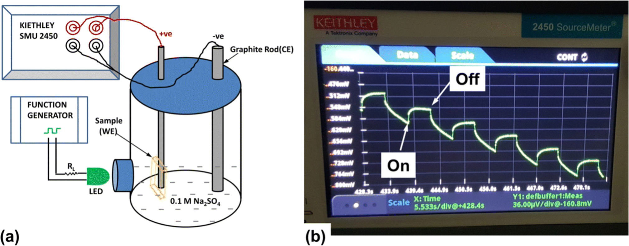
5.5. Photoelectrochemical characterization
The photo-responsive performance of m-SILAR grown Cu2O/FTO electrodes was studied by Farhad and co-workers, through transient surface photovoltage under periodic illumination of a green LED by a HITACHI VG-4429 generator with ∼0.1 Hz–square wave for ‘5 s ON and 5 s OFF’ cycle.36 The generated surface photovoltage of the Cu2O/FTO electrode was observed by a Keithley SMU 2450 by employing Cu2O/FTO thin films as a working electrode, a graphite rod as a counter electrode and 0.1 M Na2SO4 aqueous solution as an electrolyte as established in Fig. 27(a) and (b). In the presence of an aqueous electrolyte, upon 2500 s LED exposure of the photocathode, the estimated Voc for the samples grown with the non-optimized precursor, optimized precursor, and optimized precursor with CH3COOH precursor solutions, were observed as 247 ± 38 μV, 36.0 ± 2.0 mV and 47 ± 8 μV respectively. The large Voc value projected for optimized precursor film revealed a better Schottky junction produced at Cu2O/electrolyte interface, consequently, advocating a better optoelectronic quality of Cu2O thin film. The transient surface photovoltage and Voc retention for 5000 s, advocating better stability of the SILAR fabricated Cu2O thin films in aqueous electrolyte.
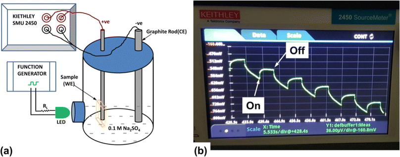 |
| | Fig. 27 (a) A representation of the transient surface photovoltage measurement system; (b) measurement of a typical Cu2O/FTO electrode in a PEC with 0.1 M Na2SO4 electrolyte followed by real-time measurement in SMU 2450 demonstrating the shape of the LED modulated transient surface photovoltage.36 | |
6. Conclusion
In summary, CuxO thin films have been extensively studied and are receiving profound attention because of their fascinating properties and promising uses in a variety of fields. In this article, an inclusive review of the state-of-the-art research activities of diverse CuxO thin films was represented based on the SILAR method. This technique has fascinated substantial attention because of its simplicity and low cost, demands less time, and is fit for the large-scale growth of CuxO. The morphology, as well as diverse properties of CuxO, can be monitored by altering the number of SILAR cycles, the pH of precursor solutions, types of salt, bath temperature, annealing, doping, and the dipping time allowed for reactions. However, the technique does not yet allow for precise control of CuxO particle sizes, which can affect the power conversion efficiency in optoelectronic devices. The main limitation of this technique is the high rate of surface roughness as well as less study of the defects in the deposited sample which is very important to control the optical as well as electrical properties in optoelectronics. Having the optimum amount of the deposited CuxO is a very significant factor in improving optoelectronic performance. Thus, the inclusion of ligands, complexing agents and surfactants in the precursor solution employed during the SILAR growth could advance the stability of CuxO. Precise control of CuxO fabrication could accelerate multiple exciton generation effects, leading to a development of overall efficiency.
Conflicts of interest
There are no conflicts to declare.
Acknowledgements
This work is funded by Comilla University and University Grants Commission, Bangladesh. The authors like to acknowledge the assistance and scientific contribution from the Department of Chemistry, Comilla University, Cumilla 3506, Bangladesh, as well as the collaborative support from the Department of Electrical and Electronics Engineering, Saga University, Japan and Center for Nanotechnology, the Department of Natural Sciences, Coppin State University, Baltimore, MD, USA.
References
- S. S. Jeong, A. Mittiga, E. Salza, A. Masci and S. Passerini, Electrodeposited ZnO/Cu2O heterojunction solar cells, Electrochim. Acta, 2008, 53, 2226–2231 CrossRef CAS.
- K. P. Musselman, A. Marin, L. Schmidt-Mende and J. L. MacManus-Driscoll, Adv. Funct. Mater., 2012, 22, 2202, DOI:10.1002/adfm.201102263.
- Q. Zhang, K. Zhang, D. Xu, G. Yang, H. Huang, F. Nie, C. Liu and S. Yang, CuO nanostructures: synthesis, characterization, growth mechanisms, fundamental properties, and applications, Prog. Mater. Sci., 2014, 60, 208–337 CrossRef CAS.
- M. K Song, S. Park, F. M. Alamgir, J. Cho and M. Liu, Nanostructured electrodes for lithium-ion and lithium-air batteries: the latest developments, challenges, and perspectives, Mater. Sci. Eng., R, 2011, 72, 203–252 CrossRef.
- V. V. Kislyuk and O. P. Dimitriev, Nanorods and nanotubes for solar cells, J Nanosci. Nanotechnol., 2008, 8, 131–148 CrossRef CAS PubMed.
- K. H. Yoon, W. J. Choi and D. H. Kang, Thin Solid Films, 2000, 372, 250, DOI:10.1016/S0040-6090(00)01058-0.
- T. Minami, Y. Nishi and T. Miyata, Efficiency enhancement using a Zn1− x Gex -O thin film as an n-type window layer in Cu2O based heterojunction solar cells, Appl. Phys. Express, 2016, 9, 052301, DOI:10.7567/APEX.9.052301.
- S. B. B. Wang, C. H. H. Hsiao, S. J. J. Chang, K. T. T. Lam, K. H. H. Wen and S. C. C. Hung, A CuO nanowire infrared photodetector, Sens. Actuators, A, 2011, 171, 207–211 CrossRef CAS.
- X. Wei, H. Zhu, T. Kong and L. Wang, Synthesis, and thermal conductivity of Cu2O nanofluids, Int. J. Heat Mass Transfer, 2009, 52, 4371–4374, DOI:10.1016/j.ijheatmasstransfer.2009.03.073.
- L. P. Zhou, B. X. Wang, X. F. Peng, X. Z. Du and Y. P. Yang, On the specific heat capacity of CuO nanofluid, Adv. Mech. Eng., 2010, 1–4 Search PubMed.
- C. Rossi, K. Zhang, D. Esteve, P. Alphonse, P. Tailhades and C. Vahlas, Nanoenergetic materials for MEMS: a review, J. Microelectromech. Syst., 2007, 16, 919–931 CAS.
- Y. W. Zhu, T. Yu, F. C. Cheong, X. J. Xu, C. T. Lim and V. B. C. Tan, Large-scale synthesis and field emission properties of vertically oriented CuO nanowire films, Nanotechnology, 2005, 16, 88–92 CrossRef CAS.
- P. S. Selvamani, J. J. Vijaya, L. J. Kennedy, B. Saravanakumar and M. Bououdina, High-performance supercapacitor based on Cu2O/MoS2/rGO nanocomposite, Mater. Lett., 2020, 275, 128095, DOI:10.1016/j.matlet.2020.128095.
- X. Zhang, W. Shi, J. Zhu, D. Kharistal, W. Zhao and B. Lalia, High-power and high-energy-density flexible pseudocapacitor electrodes made from porous CuO nanobelts and single-walled carbon nanotubes, ACS Nano, 2011, 5, 2013–2019 CrossRef CAS PubMed.
- M. M. Rahman, A. J. Saleh Ahammad, J. H. Jin, S. J. Ahn and J. J Lee, A comprehensive review of glucose biosensors based on nanostructured metal-oxides, Sensors, 2010, 10, 4855–4886 CrossRef CAS PubMed.
- Q. Huang, X. Lin, C. Lin, Y. Zhang, S. Hu and C. Wei, A high performance electrochemical biosensor based on Cu2O-carbon dots for selective and sensitive determination of dopamine in human serum, RSC Adv., 2015, 5, 54102–54108, 10.1039/C5RA05433H.
- M. Hadiyan, A. Salehi and H. Mirzanejad, Gas sensing behavior of Cu2O and CuO/Cu2O composite nanowires synthesized by template-assisted electrodeposition, J. Korean Ceram. Soc., 2021, 58, 94–105, DOI:10.1007/s43207-020-00088-z.
- K. J. Choi and H. W. Jang, One-dimensional oxide nanostructures as gas-sensing materials: review and issues, Sensors, 2010, 10, 4083–4099 CrossRef CAS PubMed.
- M. Hara, T. Kondo, M. Komoda, S. Ikeda, K. Shinohara, A. Tanaka, J. N. Kondo and K. Domen, Cu2O as a photocatalyst for overall water splitting under visible light Irradiation, Chem. Commun., 1998, 357–358, 10.1039/A707440I.
- J. Liu, J. Jin, Z. Deng, S. Z. Huang, Z. Y. Hu and L. Wang, Tailoring CuO nanostructures for enhanced photocatalytic property, J. Colloid Interface Sci., 2012, 384, 1–9 CrossRef CAS PubMed.
- I. Ali, New generation adsorbents for water treatment, Chem. Rev., 2012, 112, 5073–5091 CrossRef CAS PubMed.
- X.-Y. Yu, R.-X. Xu, C. Gao, T. Luo, Y. Jia and J.-H. Liu, Novel 3D hierarchical cotton-candy-like CuO: surfactant-free solvothermal synthesis and application in As(III) removal, ACS Appl. Mater. Interfaces, 2012, 4, 1954–1962 CrossRef CAS PubMed.
- S. Satheeskumar, S. Vadivel, K. Dhanabalan, A. Vasuhi, A. T. Ravichandran and K. Ravichandran, Enhancing the structural, optical and magnetic properties of Cu2O films deposited using a SILAR technique through Fe-doping, J. Mater. Sci.: Mater. Electron., 2018, 29, 9354–9360, DOI:10.1007/s10854-018-8966-7.
- R. Kumar, Y. Diamant and A. Gedanken, Sonochemical synthesis and characterization of nanometer-size transition metal oxides from metal acetates, Chem. Mater., 2000, 12, 2301–2305 CrossRef CAS.
- W. Shockley and H. J. Queisser, Detailed Balance Limit of Efficiency of p-n Junction Solar Cells, J. Appl. Phys., 1961, 32, 510, DOI:10.1063/1.1736034.
- A. Bhuamik, A. Haque, P. Karnati, M. F. N. Taufique, R. Patel and K. Ghosh, Copper oxide-based nanostructures for improved solar cell efficiency, Thin Solid Films, 2014, 572, 126–133, DOI:10.1016/j.tsf.2014.09.056.
- Y. C. Zhou and J. A. Switzer, Mater. Res. Innovations, 1998, 2, 22, DOI:10.1007/s100190050056.
- V. Figueiredo, E. Elangovan, G. Goncalves, N. Franco, E. Alves, S. H. K. Park, R. Martins and E. Fortunato, Phys. Status Solidi A, 2009, 206(9), 2143, DOI:10.1002/pssa.200881797.
- M. A. M. Patwary, M. Ohishi, K. Saito, Q. Guo, K. M. Yu and T. Tanaka, ECS J. Solid State Sci. Technol., 2021, 10, 065019, DOI:10.1149/2162-8777/ac0a98.
- M. A. M. Patwary, C. Y. Ho, K. Saito, Q. Guo, K. M. Yu, W. Walukiewicz and T. Tanaka, J. Appl. Phys., 2020, 127, 085302, DOI:10.1063/1.5144205.
- M. A. M. Patwary, K. Saito, Q. Guo, T. Tanaka, K. M. Yu and W. Walukiewicz, Nitrogen Doping Effect in Cu4O3 Thin Films Fabricated by Radio Frequency Magnetron Sputtering, Phys. Status Solidi B, 2020, 257(2), 1900363, DOI:10.1002/pssb.201900363.
- R. Kita, K. Kawaguchi, T. Hase, T. Koga, R. Itti and T. Morishita, J. Mater. Res., 1994, 9, 1280, DOI:10.1557/JMR.1994.1280.
- M. Y. Lin, C. Yu Lee, S. C. Shiu, I. J. Wang, J. Yu Sun, W. H. Wu, Y. Hong Lin, J. S. Huang and C. F. Lin, Sol–gel processed CuOx thin film as an anode interlayer for inverted polymer solar cells, Organ. Electron., 2010, 11, 1828–1834 CrossRef CAS.
- L. Zheng and X. Liu, Solution-phase synthesis of CuO hierarchical nanosheets at near-neutral pH and near-room
temperature, Mater. Lett., 2007, 61, 2222–2226, DOI:10.1016/j.matlet.2006.08.063.
- S. Baturay, A. Tombak, D. Batibay and Y. S. Ocak, n-Type conductivity of CuO thin films by metal doping, Appl. Surf. Sci., 2019, 477, 91–95, DOI:10.1016/j.apsusc.2017.12.004.
- S. F. U. Farhad, M. A. Hossain, N. I. Tanvir, R. Akter, M. A. M. Patwary, M. Shahjahan and M. A. Rahman, Structural, optical, electrical, and photo electrochemical properties of cuprous oxide thin films grown by modified SILAR method, Mater. Sci. Semicond. Process., 2019, 95, 68–75, DOI:10.1016/j.mssp.2019.02.014.
- S. F. U. Farhad, S. Majumder, M. A. Hossain, N. I. Tanvir, R. Akter and M. A. M. Patwary, Effect of Solution pH and Post-annealing temperatures on the Optical Bandgap of the Copper Oxide Thin Films Grown by modified SILAR Method, MRS Adv., 2019, 4(16), 937–944, DOI:10.1557/adv.2019.139.
- L. S. Huang, S. G. Yang, T. Li, B. X. Yu, Y. W. Du, Y. N. Lu and S. Z. Shi, J. Cryst. Growth, 2004, 260, 130, DOI:10.1016/j.jcrysgro.2003.08.012.
- T. Maruyama, Jpn J. Appl. Phys., 1998, 37, 4099, DOI:10.1143/JJAP.37.4099.
- B. C. Ghos, S. F. U. Farhad, M. A. M. Patwary, S. Majumder, M. A. Hossain, N. I. Tanvir, M. A. Rahman, T. Tanaka and Q. Guo, Influence of the Substrate, Process Conditions and Post-annealing Temperature on the Properties of ZnO Thin Films Grown by the Successive Ionic Layer Adsorption and Reaction Method, J. ACS Omega, 2021, 6(4), 2665–2674, DOI:10.1021/acsomega.0c04837.
- B. K. Meyer, A. Polity, D. Reppin, M. Becker, P. Hering, P. J. Klar, Th. Sander, C. Reind, J. Benz, M. Eickhoff, C. Heiliger, M. Heinemann, J. Blä sing, A. Krost, S. Shokovets, C. Mü ller and C. Ronning, Binary copper oxide semiconductors: From materials towards devices, Phys. Status Solidi B, 2012, 249(8), 1487–1509, DOI:10.1002/pssb.201248128.
- M. Heinemann, B. Eifert and C. Heiliger, Band structure and phase stability of the copper oxides Cu2O, CuO, and Cu4O3, Phys. Rev. B: Condens. Matter Mater. Phys., 2013, 87, 115111 CrossRef.
- M. F. Al-kuhaili, Characterization of copper oxide thin films deposited by the thermal evaporation of cuprous oxide (Cu2O), Vacuum, 2008, 82, 623–629, DOI:10.1016/j.vacuum.2007.10.004.
- V. Sravanthi1, T. Srikanth, A. S. Reddy, P. S. Reddy and C. S. Reddy, Electron Beam Evaporated Copper Oxide Thin Films, IOSR J. Eng., 2018, 8, 82–87 Search PubMed.
- S. F. U. Farhad, D. Cherns, J. A. Smith, N. A. Fox and D. J. Fermín, Pulsed laser deposition of single-phase n- and p-type Cu2O thin films with low resistivity, Mater. Des., 2020, 193, 108848, DOI:10.1016/j.matdes.2020.108848.
- K. Kawaguchi, R. Kita, M. Nishiyama and T. Morishita, Molecular beam epitaxy growth of CuO and Cu2O films with controlling the oxygen content by the flux ratio of Cu/O+, J. Crystal Growth, 1994, 143, 221–226, DOI:10.1016/0022-0248(94)90059-0.
- H. Uchiyama, Y. Hasegawa, H. Morita, A. Kurokouchi, K. Wada and T. Komine, Thermoelectric property of Cu2O thin film deposited by Reactive Ion Plating method, 25th International Conference on Thermoelectrics, 2006, pp. 379–381, DOI:10.1109/ICT.2006.331276.
- C. L. Chu, H. C. Lu, C. Y. Lo, C. Y. Lai and Y. H. Wang, Physical properties of copper oxide thin films prepared by dc reactive magnetron sputtering under different oxygen partial pressures, Phys. B, 2009, 404, 4831–4834, DOI:10.1016/j.physb.2009.08.185.
- A. H. Shukor, H. A. Alhattab and I. Takano, Electrical and optical properties of copper oxide thin films prepared by DC magnetron sputtering, J. Vac. Sci. Technol., B: Nanotechnol. Microelectron.: Mater., Process., Meas., Phenom., 2020, 38, 012803, DOI:10.1116/1.5131518.
- M. A. M. Patwary, K. Saito, Q. Guo and T. Tanaka, Influence of oxygen flow rate and substrate positions on properties of Cu-oxide thin films fabricated by radio frequency magnetron sputtering using pure Cu target, Thin Solid Films, 2019, 675, 59–65, DOI:10.1016/j.tsf.2019.02.026.
- D. S. C. Halin, I. A. Talib, A. R. Daud and M. A. A. Hamid, Effect of Annealing Atmosphere on the Morphology of Copper OxideThin Films Deposited on TiO2 Substrates Prepared by Sol-Gel Process, Key Eng. Mater., 2013, 594–595, 113–117, DOI:10.4028/KEM.594-595.113.
- Y. F. Lim, C. S. Chua, C. J. J. Lee and D. Chi, Sol–gel deposited Cu2O and CuO thin films for photocatalytic water splitting, Phys. Chem. Chem. Phys., 2014, 16, 25928–25934, 10.1039/C4CP03241A.
- P. B. Ahirrao, B. R. Sankapal and R. S. Patil, Nanocrystalline p-type-cuprous oxide thin films by room temperature chemical bath deposition method, J. Alloys Compd., 2011, 509, 5551–5554, DOI:10.1016/j.jallcom.2011.02.016.
- J. Y. Yao, L. Yan, G. Y. Peng, M. D. Qing and Z. F. Xin, Photoelectric properties of Cu2O thin films prepared by room-temperature water bath, Mater. Res. Express, 2017, 4, 036404, DOI:10.1088/2053-1591/aa6021.
- W. H. Lan, C. W. Tsai, S. Y. Lee, W. M. Chao, M. C. Shih, Y. C. Chou, Y. D. Wu, Y. T. Hsu, Electrical properties of cuprous oxide thin films fabricated by ultrasonic spray pyrolysis, 17th Opto-Electronics and Communications Conference, 2012, pp. 669–670, DOI:10.1109/OECC.2012.6276783.
- T. Kosugi and S. Kaneko, Novel Spray-Pyrolysis Deposition of Cuprous Oxide Thin Films, J. Am. Ceram. Soc., 1998, 81(12), 3117–3124, DOI:10.1111/j.1151-2916.1998.tb02746.x.
- S. Bijani, L. Martínez, M. Gabás, E. A. Dalchiele and J. R. R. Barrado, Low-Temperature Electrodeposition of Cu2O Thin Films: Modulation of Micro-Nanostructure by Modifying the Applied Potential and Electrolytic Bath pH, J. Phys. Chem. C, 2009, 113, 19482–19487, DOI:10.1021/jp905952a.
- M. A. Hossain, R. Al-Gaashani, H. Hamoudi, M. J. Al Marri, I. A. Hussein, A. Belaidi, B. A. Merzougui, F. H. Alharbi and N. Tabet, Controlled growth of Cu2O thin films by electrodeposition approach, Mater. Sci. Semicond. Process., 2017, 63, 203–211, DOI:10.1016/j.mssp.2017.02.012.
- W. Zhao, W. Fu, H. Yang, C. Tian, M. Li, Y. Li, L. Zhang, Y. Sui, X. Zhou, H. Chen and G. Zou, Electrodeposition of Cu2O films and their photoelectrochemical properties, CrystEngComm, 2011, 13, 2871–2877, 10.1039/C0CE00829J.
- W. Siripala, Electrodeposition of n-type Cuprous Oxide Thin Films, ECS Trans., 2008, 11(9), 1–10 CrossRef CAS.
- T. Maruyama, Copper oxide thin films prepared by chemical vapor deposition from copper dipivaloylmethanate, Sol. Energy Mater. Sol. Cells, 1998, 56, 85–92, DOI:10.1016/S0927-0248(98)00128-7.
- D. Chua, S. B. Kim, K. Li and R. Gordon, Low temperature chemical vapor deposition of cuprous oxide thin films using a Copper(I) amidinate precursor, ACS Appl. Energy Mater., 2019, 2(11), 7750–7756, DOI:10.1021/acsaem.9b01683.
- S. Eisermann, A. Kronenberger, A. Laufer, J. Bieber, G. Haas, S. Lautenschlager, G. Homm, P. J. Klar and B. K. Meyer, Phys. Status Solidi A, 20121, 209(3), 531–536, DOI:10.1002/pssa.201127493.
- T. Iivonen, M. J. Heikkila, G. Popov, H. E. Nieminen, M. Kaipio, M. Kemell, M. Mattinen, K. Meinander, K. Mizohata, J. Raisanen, M. Ritala and M. Leskela, Atomic Layer Deposition of Photoconductive Cu2O Thin Films, ACS Omega, 2019, 4(6), 11205–11214, DOI:10.1021/Facsomega.9b01351.
- A. Tamm, A. Tarre, V. Verchenko and H. S. R. Stern, Atomic Layer Deposition of Superconducting CuO Thin Films on Three-Dimensional Substrates, Crystals, 2020, 10(8), 650–659, DOI:10.3390/cryst10080650.
- Y. F. Nicolau, Solution deposition of thin solid compound films by a successive ionic-layer adsorption and reaction process, Appl. Surf. Sci., 1985, 22/23, 1061–1074, DOI:10.1016/0378-5963(85)90241-7.
- G. Regmi, A. Ashok and S. Velumani, Large Area (10 x10 cm2) production of CdS buffer layer for solar cells by chemical bath method, 17th International Conference on Electrical Engineering, Computing Science and Automatic Control (CCE), 2020, pp. 1–6, DOI:10.1109/CCE50788.2020.9299158.
- P. A. Sachin, R. S. Devan, D. S. Patil, A. V. Moholkar, M. G. Gang, Y. R. Ma, J. H. Kim and P. S. Patil, Improved solar cell performance of chemo-synthesized cadmium selenide pebbles, Electrochim. Acta, 2013, 98, 244–254 CrossRef.
- F. G. Hone and T. Abza, Short review of factors affecting chemical bath deposition method for metal chalcogenide thin films, Int. J. Thin Film. Sci. Technol., 2019, 8(2), 43–53 Search PubMed.
- H. M. Pathan and C. D. Lokhande, Deposition of metal chalcogenide thin films by successive ionic layer adsorption and reaction (SILAR) method, Bull. Mater. Sci., 2004, 27, 85–111, DOI:10.1007/BF02708491.
- B. R. Sankapal, R. S. Mane and C. D. Lokhande, Successive ionic layer adsorption and reaction (SILAR) method for the deposition of large area (∼10 cm2) tin disulfide (SnS2) thin films, Mater. Res. Bull., 2000, 35(12), 2027–2035, DOI:10.1016/s0025-5408(00)00405-0.
- S. Visalakshi, R. Kannan, S. Valanarasu, A. Kathalingam and S. Rajashabala, Studies on optical and electrical properties of SILAR-deposited CuO thin films, Mater. Res. Innovations, 2016, 11(1), 146–151, DOI:10.1080/14328917.2016.1194586.
- M. Sasagawa and Y. Nosaka, Studies on the effects of Cd ion sources and chelating reagents on atomic layer CdS deposition by successive ionic layer adsorption and reaction (SILAR) method, Phys. Chem. Chem. Phys., 2001, 3(16), 3371–3376, 10.1039/b101075l.
- P. O. Oviroh, R. Akbarzadeh, D. Pan, R. A. Maarten Coetzee and T. C. Jen, New development of atomic layer deposition: processes, methods and applications, Sci. Technol. Adv. Mater., 2019, 20(1), 465–496, DOI:10.1080/14686996.2019.1599694.
- S. M. George, Atomic Layer Deposition: An Overview, Chem. Rev., 2010, 110(1), 111–131, DOI:10.1021/cr900056b.
- M. Leskelä and M. Ritala, Atomic layer deposition chemistry: Recent developments and future challenges, Angew. Chem., 2003, 42(45), 5548–5554, DOI:10.1002/anie.200301652.
- Molecular Beam Epitaxy & Atomic Layer Deposition Systems. SVT Associates.
- N. Sahu, B. Parija and S. Panigrahi, Fundamental understanding and modeling of spin coating process: A review, Ind. J. Phys., 2009, 83(4), 493–502 CrossRef CAS.
- A. N. Nguyen, J. Solard, H. T. Nong, C. B. Osman, A. Gomez, V. Bockelée, S. Tencé-Girault, F. Schoenstein, M. Simón-Sorbed, A. E. Carrillo and S. Mercone, Spin Coating and Micro-Patterning Optimization of Composite Thin Films Based on PVDF, Materials, 2020, 13, 1342 CrossRef CAS PubMed.
- M. D. Tyona, A theoretical study on spin coating technique, Adv. Mater. Res., 2013, 2(4), 195–208, DOI:10.12989/amr.2013.2.4.195.
- https://www.ossila.com/pages/spin-coating.
- N. Asim, S. Ahmadi, M. A. Alghoul, F. Y. Hammadi, K. Saeedfar and K. Sopian, Research and development aspects on chemical preparation techniques of photoanodes for dye sensitized solar cells, Int. J. Photoenergy, 2014, 2014, 518156 CrossRef.
- Y. Wang and A. Hu, Carbon quantum dots: synthesis, properties and applications, J. Mater. Chem. C, 2014, 2, 6921–6939, 10.1039/C4TC00988F.
- B. R. Sankapal, A. Ennaoui, T. Guminskaya, T. Dittrich, W. Bohne, J. Röhrich, E. Strub and M. Ch. Lux-Steiner, Characterization of p-CuI prepared by the SILAR technique on Cu-tape/n-CuInS2 for solar cells, Thin Solid Films, 2005, 480–481, 142–146, DOI:10.1016/j.tsf.2004.11.020.
- H. M. Pathan and C. D. Lokhande, Deposition of metal chalcogenide thin films by successive ionic layer adsorption and reaction (SILAR) method, Bull. Mater. Sci., 2004, 27, 85–111, DOI:10.1007/BF02708491.
- S. S. Oluyamo, M. S. Nyagba, S. Ambrose and S. Ojo, Optical properties of copper(I) oxide thin films synthesized by SILAR technique, IOSR J. Appl. Phys., 2014, 6, 102–110, DOI:10.9790/4861-0631102105.
- K. Mageshwari and R. Sathyamoorthy, Physical properties of nanocrystalline CuO thin films prepared by the SILAR method, Mater. Sci. Semicond. Process., 2012, 16, 337–343, DOI:10.1016/j.mssp.2012.09.016.
- M. Mehrabian, Optical and photovoltaic properties of ZnS nanocrystals fabricated on Al:ZnO films using the SILAR technique, J. Opt. Technol., 2016, 83, 422–428 CrossRef CAS.
- C. García, S. Dávila, G. Jardón, F. Flores, R. Bon and Y. V. Vorobiev, Characterization of PbS films deposited by successive ionic layer adsorption and reaction (SILAR) for CdS/PbS solar cells application, Mater. Res. Express, 2020, 7, 015530, DOI:10.1088/2053-1591/ab6b5c.
- K. Manikandan, C. Dilip, P. Mani and J. J. prince, Deposition and Characterization of CdS Nano Thin Film with Complexing Agent Triethanolamine, American Journal of Engineering and Applied Sciences, 2015, 8, 318–327, DOI:10.3844/AJEASSP.2015.318.327.
- M. Ristov and G. Sinadinovski, Chemical deposition of Cu2O thin films, Thin Solid Films, 1985, 123, 63–67 CrossRef CAS.
- M. T. S. Nair, L. Guerrero, O. L. Arenas and P. K. Nair, Chemically deposited copper oxide thin films: structural, optical and electrical characteristics, Appl. Surf. Sci., 1999, 150, 143–151, DOI:10.1016/S0169-4332(99)00239-1.
- M. A. Hossain, S. F. U. Farhad, N. I. Tanvir, J. H. Chang, M. A. Rahman, T. Tanaka, Q. Guo, J. Uddin and M. A. M. Patwary, R. Soc. Open Sci., 2022, 9, 211899, DOI:10.1098/rsos.211899.
- R. D. Umeri, R. U. Osuji and F. I. Ezema, Synthesis and characterization of copper oxide thin films using successive ionic layer adsorption reaction (SILAR) method, J. Chem. Mater. Res., 2016, 8(6), 68–76 Search PubMed.
- Y. Liu, Y. Chu, Y. Zhuo, M. Li, L. Li and L. Dong, Anion-controlled construction of CuO honeycombs and flowerlike assemblies on copper foils, Cryst. Growth Des., 2007, 7(3), 467–470, DOI:10.1021/cg060480r.
- G. Altindemir and C. Gumus, Cu2O thin films prepared by using four different copper salts at a low temperature: An investigation of their physical properties, Mater. Sci. Semicond. Process., 2020, 107, 104805 CrossRef CAS.
- S. Chatterjee, S. K. Saha and A. J. Pal, Formation of all-oxide solar cells in atmospheric condition based on Cu2O thin-films grown through SILAR technique, Sol. Energy Mater. Sol. Cells, 2016, 147, 17–26 CrossRef CAS.
- M. Yuksel, J. R. Pennings, F. Bayansal and J. T. W. Yeow, Effect of B-doping on the morphological, structural and optical properties of SILAR deposited CuO films, Phys. B, 2020, 599, 412578, DOI:10.1016/j.physb.2020.412578.
- A. A. Lobinsky and M. V. Kaneva, Synthesis Ni-doped CuO nanorods via Successive Ionic Layer Deposition method and their capacitive performance, Nanosyst.: Phys., Chem., Math., 2020, 11(5), 608–614, DOI:10.17586/2220-8054-2020-11-5-608-614.
- H. M. Pathan and C. D. Lokhande, Deposition of metal chalcogenide thin films by successive ionic layer adsorption and reaction (SILAR) method, Bull. Mater. Sci., 2004, 27, 85–111, DOI:10.1007/BF02708491.
- S. Majumder, N. I. Tanvir, B. C. Ghos, M. A. M. Patwary, M. A. Rahman, M. A. Hossain and S. F. U. Farhad, Optimization of the growth conditions of Cu2O thin films and subsequent fabrication of Cu2O/ZnO heterojunction by m-SILAR method, WIECON-ECE, 2020, DOI:10.1109/WIECON-ECE52138.2020.9397989.
- M. Ristov and G. Sinadinovski, Chemical deposition of Cu2O thin films, Thin Solid Films, 1985, 123, 63–67 CrossRef CAS.
- S. Visalakshi, R. Kannan, S. Valanarasu, A. Kathalingam and S. Rajashabala, Studies on optical and electrical properties of SILAR-deposited CuO thin films, Mater. Res. Innovations, 2016, 11(1), 146–151, DOI:10.1080/14328917.2016.1194586.
- V. Saravanakannan and T. Radhakrishnan, Structural, electrical and optical characterization of Cuo thin films prepared by spray pyrolysis technique, Int. J. Chem. Tech. Res., 2014, 6, 306–310 Search PubMed.
- O. Gençyılmaz and T. Taşköprü, Effect of pH on the synthesis of CuO films by SILAR method, J. Alloys Compd., 2016, 695, 1205–1212, DOI:10.1016/j.jallcom.2016.10.247.
- N. Soundaram, R. Chandramohan, S. Valanarasu, R. Thomas and A. Kathalingam, Studies on SILAR deposited Cu2O and ZnO films for solar cell applications, J. Mater. Sci.: Mater. Electron., 2015, 26, 5030–5036, DOI:10.1007/s10854-015-3020-5.
- D. Ozaslan, O. M. Ozkendir, M. Gunes, Y. Ufuktepe and C. Gumus, Study of the electronic properties of Cu2O thin films by X-ray absorption spectroscopy, Optik, 2018, 157, 1325–1330, DOI:10.1016/j.ijleo.2017.12.119.
- O. Daoudi, A. Elmadani, M. Lharch and M. Fahoume, A new efficient synthesis of CuO thin films using modified SILAR method, Opt. Quantum Electron., 2020, 52, 413, DOI:10.1007/s11082-020-02530-2.
- K. Mageshwari and R. Sathyamoorthy, Physical properties of nanocrystalline CuO thin films prepared by the SILAR method, Mater. Sci. Semicond. Process., 2013, 16(2), 337–343 CrossRef CAS.
- O. Daoudi, Y. Qachaou, A. Raidou, K. Nouneh, M. Lharch and M. Fahoume, Study of the Physical Properties of CuO Thin Films Grown by Modified SILAR Method for Solar Cells Applications, Superlattices Microstruct., 2018, 127, 93–99, DOI:10.1016/j.spmi.2018.03.006.
- M. T. S. Nair, L. Guerrero, O. L. Arenas and P. K. Nair, Chemically deposited copper oxide thin films: structural, optical and electrical characteristics Applied Surface Science, 1999, 150, 143–151 CrossRef CAS.
- F. Baig, Y. H. Khattaka, B. M. Soucasea, S. Beg and S. Ullah, Effect of anionic bath temperature on morphology and photo-electrochemical properties of Cu2O deposited by SILAR, Mater. Sci. Semicond. Process., 2018, 88, 35–39, DOI:10.1016/j.mssp.2018.07.031.
- F. Bayansal, S. Kahraman, G. Cankaya, H. S. Guder and H. M. Cakmar, Growth of homogenous CuO nano-structured thin films by a simple solution method, J. Alloys Compd., 2011, 509, 2094–2098, DOI:10.1016/j.jallcom.2010.10.146.
- V. Rajendran, J Gajendiran, Preparation, and characterization of nanocrystalline CuO powders with the different surfactants and complexing agent mediated precipitation method, Mater. Res. Bull., 2014, 56, 2014134–2014137, DOI:10.1016/J.MATERRESBULL.2014.05.002.
- F. Bayansal, B. Sahin, M. Yüksel, N. Biyikli, H. A. Çetinkara and H. S. Güder, Influence of coumarin as an additive on CuO nanostructures prepared by successive ionic layer adsorption and reaction (SILAR) method, J. Alloys Compd., 2013, 566, 78–82, DOI:10.1016/j.jallcom.2013.03.018.
- F. Bayansal, B. Sahin, M. Yuksel and H. A. Cetinkara, SILAR-based growth of nanostructured CuO thin films from alkaline baths containing saccharin as additive, Mater. Lett., 2013, 98, 197–200, DOI:10.1016/j.matlet.2013.02.030.
- R. Aydin and H. Cavusoglu, Influence of sodium dodecyl sulfate as a surfactant on the microstructural, morphological and optoelectronic characteristics of SILAR deposited CuO thin films, Mater. Res. Express, 2019, 6, 086403, DOI:10.1088/2053-1591/ab1a08.
- H. Cavusoglu and R. Aydin, Complexing agent triethanolamine mediated synthesis of nanocrystalline CuO thin films at room temperature via SILAR technique, Superlattices Microstruct., 2019, 128, 37–47, DOI:10.1016/j.spmi.2019.01.011.
- K. Amudhavalli, N. Neelakandapillai and M. Nagarajan, Synthesis of Cu2O by SILAR and the impact of Annealing on the Structural Properties, Int. J. Sci. Eng. Manage., 2018, 3, 494–497 Search PubMed.
- N. Serin, T. Serin, S. Horzum and Y. Celik, Annealing effects on the properties of copper oxide thin films prepared by chemical deposition, Semicond. Sci. Technol., 2005, 20, 398–401 CrossRef CAS . https://iopscience.iop.org/0268-1242/20/5/012.
- M. R. Johan, M. S. M. Suan, N. L. Hawari and H. A. Ching, Annealing Effects on the Properties of Copper Oxide Thin Films Prepared by Chemical Deposition, Int. J. Electrochem. Sci., 2011, 6, 6094–6104 CAS.
- M. T. S. Nair, L. Guerrero, O. L. Arenas and P. K. Nair, Chemically deposited copper oxide thin films: structural, optical and electrical characteristics, Appl. Surf. Sci., 1999, 150, 143–151 CrossRef CAS.
- D. Ozaslan, O. Erken, M. Gunes and C. Gumus, The effect of annealing temperature on the physical properties of Cu2O thin film deposited by SILAR method, Phys. B, 2020, 580, 411922, DOI:10.1016/j.physb.2019.411922.
- S. Chatterjee, S. K. Saha and A. J. Pal, Sol. Energy Mater. Sol. Cells, 2016, 147, 17 CrossRef CAS.
- M. Abdel Rafea and N. Roushdy, Determination of the optical band gap for amorphous and nanocrystalline copper oxide thin films prepared by SILAR technique, J. Phys. D: Appl. Phys., 2009, 42, 015413 CrossRef , p. 6..
- T. C. Tasdemirci, Copper Oxide Thin Films Synthesized by SILAR: Role of Varying Annealing Temperature, Electron. Mater. Lett., 2020, 16, 239–246, DOI:10.1007/s13391-020-00205-4.
- K. Dhanabalan, A. T. Ravichandran, K. Ravichandran, S. Valanarasu and S. Mantha, Effect of Co doped material on the structural, optical and magnetic properties of Cu2O thin films by SILAR technique, J. Mater. Sci.: Mater. Electron., 2016, 28, 4431–4439, DOI:10.1007/s10854-016-6072-2.
- S. Satheeskumar, S. Vadivel, K. Dhanabalan, A. Vasuhi, A. T. Ravichandran and K. Ravichandran, Enhancing the structural, optical and magnetic properties of Cu2O films deposited using a SILAR technique through Fe-doping, J. Mater. Sci.: Mater. Electron., 2018, 29, 9354–9360, DOI:10.1007/s10854-018-8966-7.
- N. Soundaram, R. Chandramohan, R. David Prabu, S. Valanarasu, K. Jeyadheepan, A. Kathalingam, M. S. Hamdy, A. M. Alhanash and K. S. Al-Namshah, Preparation of Eu-doped Cu2O thin films using different concentrations by SILAR and their heterojunction property with ZnO, J. Electron. Mater., 2019, 48, 4138–4147, DOI:10.1007/s11664-019-07174-x.
- A. T. Ravichandran, K. Dhanabalan, K. Ravichandran, R. Mohan, K. Karthika, A. Vasuhi and B. Muralidharan, Tuning the structural and optical properties of SILAR-deposited Cu2O films through Zn doping, Acta Metall. Sin., 2019, 28(8), 1041–1046, DOI:10.1007/s40195-015-0292-y.
- M. Yuksel, J. R. Pennings, F. Bayansal and J. T. W. Yeow, Effect of B-doping on the morphological, structural and optical properties of SILAR deposited CuO films, Phys. B, 2020, 599, 412578, DOI:10.1016/j.physb.2020.412578.
- F. Bayansal, T. TaşKöPrü, B. Nyamin ŞAhin and H. A. C. Etinkara, The Minerals, Metals & Materials Society and ASM International, 2014 Search PubMed.
- Y. Gülen, F. Bayansal, B. Sahin, H. A. Cetinkara and H. S. Güder, SciVerse ScienceDirect, 2013 Search PubMed.
- F. Bayansal, Y. Gülen, B. Sahin, S. Kahraman and H. A. Çetinkara, CuO nanostructures grown by the SILAR method: influence of Pb-doping on the morphological, structural and optical properties, J. Alloys Compd., 2014, 619, 378–382, DOI:10.1016/j.jallcom.2014.09.085.
- A. A. Lobinsky and M. V. Kaneva, Synthesis Ni-doped CuO nanorods via Successive Ionic Layer Deposition method and their capacitive performance, Nanosyst.: Phys., Chem., Math., 2020, 11(5), 608–614 CAS.
- J. Katayama, K. Ito, M. Matsuoka and J. Tamaki, Performance of Cu2O/ZnO solar cell prepared by two-step electrodeposition, J. Appl. Electrochem., 2004, 34, 687 CrossRef CAS.
- S. Shyamal, P. Hajra, H. Mandal, A. Bera, D. Sariket, A. K. Satpati, M. V. Malashchonak, A. V. Mazanik, O. V. Korolik, A. I. Kulak, E. V. Skorb, A. Maity, E. A. Streltsov and C. Bhattacharya, Chem. Eng. J., 2018, 335, 676 CrossRef CAS.
- N. H. Ke, P. T. K. Loan, D. A. Tuan, H. T. Dat, C. V. Tran and L. Y. T. Hung, The characteristics of IGZO/ZnO/Cu2O:Na thin film solar cells fabricated by DC magnetron sputtering method, J. Photochem. Photobiol., A, 2017, 349, 100, DOI:10.1016/j.jphotochem.2017.09.016.
- D. P. Joseph, T. P. David, S. P. Raja and C. Venkateswaran, Mater. Charact., 2008, 59, 1137 CrossRef CAS.
- J. Antony, Y. Qiang, M. Faheem, D. Meyer, D. E. McCready and M. H. Engelhard, Ferromagnetic semiconductor nanoclusters: Co-doped Cu2O, Appl. Phys. Lett., 2007, 90, 013106 CrossRef.
- S. Chatterjee and A. J. Pal, Introducing Cu2O thin films as a hole-transport layer in efficient planar perovskite solar cell structures, J. Phys. Chem. C, 2016, 120, 1428, DOI:10.1021/acs.jpcc.5b11540.
- M. R. Das, A. Mukherjee, P. Maiti, S. Das and P. Mitra, Studies on multifunctional properties of SILAR synthesized CuO thin films for enhanced supercapacitor, photocatalytic and ethanol sensing applications, J. Electron. Mater., 2019, 48, 2718–2730, DOI:10.1007/s11664-019-06940-1.
- G. S. Gund, D. P. Dubal, S. S. Shinde and C. D. Lokhande, Architectured Morphologies of Chemically Prepared NiO/MWCNTs Nanohybrid Thin Films for High Performance Supercapacitors, ACS Appl. Mater. Interfaces, 2014, 6, 3176, DOI:10.1021/am404422g.
- X. Zhong, H. He, J. Du, Q. Ren, J. Huang, Y. Tang, J. Wang, L. Yang, F. Dong and L. Bian, Boosting solar water oxidation activity and stability of BiVO4 photoanode through the Co-catalytic effect of CuCoO2, Electrochim. Acta, 2019, 304, 301, DOI:10.1016/j.electacta.2019.02.101.
- B. Sahin and T. Kaya, Facile preparation and characterization of nanostructured ZnO/CuO composite thin film for sweat concentration sensing applications, Mater. Sci. Semicond. Process., 2021, 121, 105428, DOI:10.1016/j.mssp.2020.105428.
- K. Dhanabalan, A. T. Ravichandran, A. Vasuhi, R. Chandramohan, P. Karthick and S. Mantha, Effect of annealing based on the structural, optical, morphological and antibacterial activities of copper oxide thin films by SILAR technique, Int. J. Thin Films Sci. Technol., 2022, 11(1), 65–72, DOI:10.18576/ijtfst/110108.
- V. Scuderi, G. Amiard, S. Boninelli, S. Scalese, M. Miritello, P. M. Sberna, G. Impellizzeri and V. Privitera, Photocatalytic activity of CuO and Cu2O nanowires, Mater. Sci. Semicond. Process., 2016, 42, 89–93 CrossRef CAS.
- X. Bai, L. Ma, Z. Dai and H. Shi, Electrochemical synthesis of p-Cu2O/n-TiO2 heterojunction electrode with enhanced photoelectrocatalytic activity, Mater. Sci. Semicond.
Process., 2018, 74, 319–328 CrossRef CAS.
- A. S. Patil, M. D. Patil1, G. M. Lohar, S. T. Jadhav and V. J. Fulari, Super capacitive properties of CuO thin films using modified SILAR method, Ionics, 2016, 23, 1–8, DOI:10.1007/s11581-016-1921-9.
- V. S. Kumbhar, A. C. Lokhande, N. S. Gaikwad and C. D. Lokhande, One-step chemical synthesis of samarium telluride thin films and their supercapacitive properties, Chem. Phys. Lett., 2016, 645, 112–117, DOI:10.1016/j.cplett.2015.12.042.
- S. A Mahadik, F. D. Pedraza and B. P. Relekar, Synthesis and characterization of superhydrophobic–superoleophilic surface, J. Sol-Gel Sci. Technol., 2016, 78, 475–481, DOI:10.1007/s10971-016-3974-7.
- W. G. Pell and B. E. Conway, Analysis of power limitations at porous supercapacitor electrodes under cyclic voltammetry modulation and dc charge, J. Power Sources, 2001, 96, 57–67, DOI:10.1016/S0378-7753(00)00682-0.
- D. P. Dubal, G. S. Gund, C. D. Lokhande and R. Holze, Decoration of sponge-like Ni(OH)2 nanoparticles onto MWCNTs using an easily manipulated chemical protocol for supercapacitors, ACS Appl. Mater. Interfaces, 2013, 5(7), 2446–2454, DOI:10.1021/am3026486.
|
| This journal is © The Royal Society of Chemistry 2022 |
Click here to see how this site uses Cookies. View our privacy policy here. 
 Open Access Article
 This Open Access Article is licensed under a
  *ab,
Md Alauddin Hossaina,
Bijoy Chandra Ghosa,
Joy Chakrabartya,
Syed Ragibul Haquec,
Sharmin Akther Rupaa,
Jamal Uddin
*ab,
Md Alauddin Hossaina,
Bijoy Chandra Ghosa,
Joy Chakrabartya,
Syed Ragibul Haquec,
Sharmin Akther Rupaa,
Jamal Uddin