DOI:
10.1039/D2RA06255K
(Paper)
RSC Adv., 2022,
12, 29805-29812
Optimized study of the annealing effect on the electrical and structural properties of HDLC thin-films
Received
5th October 2022
, Accepted 5th October 2022
First published on 18th October 2022
Abstract
The plasma-enhanced chemical vapor deposition (PECVD) technique has been utilized for the facile surface deposition of hydrogenated diamond-like carbon (HDLC) thin-films onto Si(100) substrates. The as-deposited film surface is homogenous, free of pinholes, and adheres to the substrate. Annealing of the synthesized HDLC surface in a vacuum was performed in the temperature range of 200 to 1000 °C. A host of instrumental techniques, viz. FTIR spectroscopy, AFM, STM, and EC-AFM, were successfully employed to detect the morphological transformation in the HDLC films upon annealing. EC-AFM studies show irreversible biased behavior after undergoing a surface redox couple reaction and morphological change. Raman spectroscopy was carried out along with STM and EC-AFM to determine the functional nature and conductivity of the annealed surface.
1. Introduction
For the advancement of basic solid-state material science, nanotechnology and nanoscience are largely considered major driving forces. The quality of our daily lives has improved extensively due to the discovery of novel nanomaterials, and the most important class of such nanomaterials is based on carbon. Hydrogenated diamond-like carbon (HDLC) is an artificially synthesized tetrahedral structured carbon-based nanomaterial. Its properties are similar to those of a pure diamond, which is a purely tetrahedral structure of carbon atoms. The synthesis of HDLC materials is tunable, and hence their properties are variable. The term diamond-like carbon (DLC) was first used by Aisenberg and Chabot for the ion-beam deposition of carbon thin-films.1 They immensely helped in understanding the growth mechanisms, material characteristics, and feasibility of the industrial applications of DLC. A slightly modified form of DLC, hydrogenated DLC (HDLC), does not stand for a particular composition, but it is a combination of sp2 and sp3 hybridized crystalline and amorphous carbon thin-films whose properties effectively depend on the synthetic nature and various treatments applied. Moreover, the synthesis and design characterization of a carbon-based nanocrystalline diamond can be tuned. We can change and improve the colour, hardness, sp2/sp3 ratio, etc., by varying the deposition time and flow rate of gas.2 The film can be characterized using different techniques, such as scanning probe microscopy (AFM and STM), FTIR spectroscopy, Raman spectroscopy, and EC-AFM.
Owing to the unique properties of their inherent characteristics, viz., a low coefficient of friction,3 chemical inertness, appreciable hardness, enhanced current resistance, and chemical non-reactivity, DLC films have received widespread traction in a host of commercial applications, such as biocompatible coatings in cardiac medicines and orthopedics as well as protective hard coatings in contact lenses for tribological applications. There are various industrial apparatuses as well as some tools used in everyday life, such as scissors, knives, and safety razors, that are coated with HDLC to retain their sharpness for a long period; gears, drill bits, and weapons are also coated with DLC.4
The structure, hardness, and electrical characteristics of HDLC can be significantly altered by thermal annealing.5,6 It can enhance the degree of graphitization and diminish the intrinsic compressive stress of HDLC.7,8 The thermal annealing of HDLC films and subsequent bond changes result in the cleavage of C–H bonds, leading to hydrogen depreciation. All these phenomena lead to an increase in the sp2 content of the film, and when the sp2 clusters are finally enough for overlap, the band gap diminishes, which improves the conductive nature of the material. This creates a scientific interest in their electronic applications. The knowledge of their electronic properties, such as the carrier mobilities, change in work function, and temperature-dependent Hall effect due to graphitization, informs us of the possible applications of HDLC films in electronic devices. Some other applications of HDLC materials are in forming tools for deep drawing,9 active sensors,10 corrosion resistance,11 biomedical implants and instruments,12 surface coatings for coronary stents,13 heart valves, orthopedic implants,14 magnetic storage devices, and micro-electromechanical devices (MEMS).15
2. Experimental section
2.1 Materials
Potassium ferrocyanide (K4[Fe(CN)6]·3H2O; MW 368.32; 99.96%; Sisco Research Laboratories Pvt Ltd), helium gas (He; 99.999%; Hindustan Gases & Welding Com), methane (CH4; 99%; Praxair India Pvt. Ltd), and p-type mirror-polished Si(100) wafers were used in the experiments. Ultrapure water from the Milli-Q system (Millipore Co.) was used throughout the experiments.
2.2 Film deposition and annealing
The simple preparation of HDLC thin-films via the reduced pressure enhanced nucleation (BEN) method16 at normal temperature in an asymmetrically capacitive RF (13.56 MHz) combined tool17 involves the following two steps: (1) etching of the mirror-polished Si(100) substrate with a 20 mm diameter for 1200 s in pure hydrogen (flow rate ∼ 500 cm3 min−1) plasma, at a pressure of 0.0193 kPa, produced by a 30 W RF power-producing dc self-negative bias (∼−200 V), to remove the oxide layer from the surface of Si (100); and (2) the in situ BEN process16 using He (flow rate ∼ 1500 cm3 min−1) plasma produced by a 50 W RF power-producing dc self-negative bias (∼−200 V), with H2 (flow rate ∼ 500 cm3 min−1) and CH4 (flow rate ∼ 50 cm3 min−1) gases at a total pressure of 0.0756 kPa and at a substrate temperature of ∼287 K for 1800 s deposition time. The as-prepared film18 was annealed at constant temperatures of 200 °C, 400 °C, 700 °C, and 1000 °C for ∼1800 s at a high vacuum (∼1.3 × 10⁻⁴ Pa) and cooled to ∼27 °C.
2.3 Instrumental
Raman spectra were obtained on a confocal micro-Raman spectrometer (LabRAM HR Vis., Horiba Jobin Yvon S.A.S), which includes an 800 mm focal length Czerny–Turner-type spectrograph equipped with mirrors (reflective optics) with a high spectral resolution of 0.1 cm−1 per pixel at 488 nm with an 1800 g mm−1 gratin. Atomic force microscopy (AFM) topography of the sample was performed in the non-contact mode with a Si3N4 cantilever using a multimode scanning probe microscope (Agilent AFM 5500 series system, USA) with a multipurpose small scanner with a low coherence laser (1 mW power, 670 nm wavelength (<50 μm), scan range XY: 0–10 μm; Z: 0–2 μm; noise level: XY < 0.1 nm RMS, Z < 0.02 nm RMS). Using scanning tunneling microscopy (STM) under the constant-tunneling-current mode with a pre-cut 80% platinum–20% iridium Agilent STM tip, the topography of the sample was obtained using a multimode scanning probe microscope (Agilent AFM 5500 series system, USA) with a multipurpose small scanner with a scan range Z of 0–2 mm and a noise level Z of <0.02 nm RMS. In this instrument, a feedback loop maintained a constant tunneling current during scanning by vertically moving the scanner at each (X–Y) data point until reaching a given set-point value (0.5 nano Ampere). The computer stores the vertical position of the scanner at each (X–Y) datum to form a topographic image of the sample surface, that is, whether it is conductive or semiconducting. A potentiostat/galvanostat coupled with an AFM (EC-AFM, Agilent AFM 5500 series system, PicoScan Software, USA) was used to perform electrochemical cyclic voltammetry experiments on the HDLC thin-film surface, which was the working electrode. The working electrode was connected through an L-shaped pogo electrode. The pogo contacts the sample working electrode through a separate access hole outside the liquid cell chamber. Moreover, it is not in contact with the electrolyte and does not require any special cleaning. A platinum–iridium counter electrode (CE) encompasses as much of the inner rim of the liquid cell as possible. The reference electrode (RE) is located within the electrolyte but is not in contact with the working electrode. Using cyclic voltammetry between the potentials of −1.0 and +1.0 V, the experiment was run in EC-AFM14,15 with different scan rates (mV s−1) using the [Fe(CN)6]4−/[Fe(CN)6]3− redox couple in an unperturbed solution of 1 mM ferricyanide dissolved in 0.1 M H2SO4 solution on the HDLC film. The surface morphology during electrochemical change was investigated using AFM in situ in the non-contact mode. The Fourier transform infrared (FTIR) spectrum of the sample was obtained on an infrared Fourier vacuum prism spectroscope Vertex 70v (Bruker Optik GmbH Germany) with ATR crystal (Zn–Se) for the solid HDLC samples. A KBr beam splitter, DLaTGS detector, MIR source, Rock Solid measuring device system, spectral resolution of >0.4 cm−1), and contamination-free vacuum (<0.2 mbar) are the key technical features of a Vertex 70v. To distinguish the transformational change and calculate the bonded hydrogen content due to the annealing of the HDLC structure, an FTIR spectrophotometer was employed.
3. Results and discussion
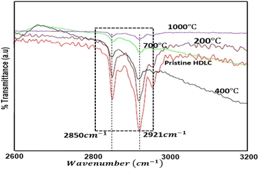
The FTIR spectra of the annealed HDLC films are shown in Fig. 1. A couple of characteristic absorption peaks of the HDLC films could be observed at 2850 and 2921 cm−1 owing to the hybridized sp3 C–H arrangement.19 Because these peaks are attributed to the attachment of H to carbon preferring the sp3 structure more than sp2, no other peak is recorded. The intensity of percentage transmittance changes reduces as the annealing temperature rises. This observation is attributed to the change in the hydrogen content in the films due to the tempering or diminishing sp3 content in the HDLC films.
 |
| | Fig. 1 FTIR spectra of pristine HDLC and annealed HDLC thin-films at different temperatures. | |
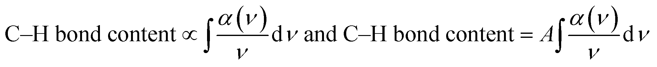
It is well known that igniting non-crystalline carbon films leads to a preferential release of hydrogen, which is the foundation of structural modification. Some authors report a similar decrease in the intensities of the aforementioned peaks.20–23 Significantly, after annealing, there is no marked shift in the peak position. This implies that the interatomic space between C and H is unchanged after annealing. The net H content present in the films accounts for the cumulatively bonded hydrogens, those directly adhered to the carbon atoms, and those indirectly bound to the carbon atoms.7 Some direct methods have been used to measure the H-content in diamond films, such as ERDA and NRA,24 and other methods, such as NMR and IR absorption, can be used to monitor the H-content in diamond-like materials indirectly compared with the NRA method.24 The effect of annealing was demonstrated using FTIR analysis herein. The total hydrogen content attached to C as C–H was estimated from the sum of the indicated areas of the infrared absorption peaks in the FTIR spectra using the following eqn (1):25
| |
 | (1) |
where
A is the proportionality factor proportional to the inverse of the oscillator length; its value changes based on the position of the absorption peak. The values of
A are 1.085 × 10
19 cm
−2 and 6.899 × 10
19 cm
−2 for the absorption peaks at 2850 cm
−1 and 2921 cm
−1, respectively,
25 and
a(
ν) is the absorption coefficient at frequency ν.
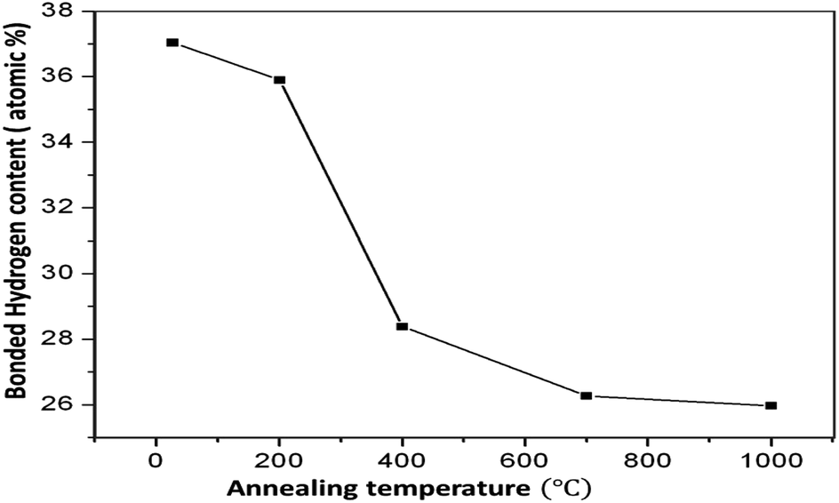
Fig. 2 shows that thermal annealing leads to an indirect quantitative measurement of the evolution of hydrogen from both groups
via the breaking of C–H bonds in the films.
 |
| | Fig. 2 Bonded hydrogen vs. annealing temperature. | |
One of the commonly used non-destructive techniques to characterize graphitic materials is Raman spectroscopy, particularly to specify the defects and disorders as well as the ordered structure of graphene and graphite-like structures. Fig. 3 shows two Raman bands, one at 1369 cm−1 (D band) and another at 1551 cm−1 (G band), which correspond to the vibrational modes of the CH and CH2 groups at 27 °C on the HDLC surface. The G band is associated with the symmetric E2g C![[double bond, length as m-dash]](https://www.rsc.org/images/entities/char_e001.gif) C stretching mode of sp2 bonding in carbonaceous materials,26 whereas the D band can be ascribed to the angle discrepancy in the graphite-like microdomains affected by the sp3 bonds or j-point phonons of A1g symmetry.27 Due to the increase in sp2 carbon after annealing, the second-order Raman (2D) spectrum increases. The intensity ratio of the D-band and G-band (ID/IG) is calculated to ascertain the microstructure of the graphite-like sheets and specify the lattice disorder. The shifting of the G and D bands with increasing ID/IG ratio due to annealing clearly indicates dehydrogenation (i.e., oxidation) of the HDLC film surface. Using the G peak position (ωG) of the Raman spectra, the sp2/sp3 ratio is estimated by the following empirical equation,27 as shown in Table 1.
C stretching mode of sp2 bonding in carbonaceous materials,26 whereas the D band can be ascribed to the angle discrepancy in the graphite-like microdomains affected by the sp3 bonds or j-point phonons of A1g symmetry.27 Due to the increase in sp2 carbon after annealing, the second-order Raman (2D) spectrum increases. The intensity ratio of the D-band and G-band (ID/IG) is calculated to ascertain the microstructure of the graphite-like sheets and specify the lattice disorder. The shifting of the G and D bands with increasing ID/IG ratio due to annealing clearly indicates dehydrogenation (i.e., oxidation) of the HDLC film surface. Using the G peak position (ωG) of the Raman spectra, the sp2/sp3 ratio is estimated by the following empirical equation,27 as shown in Table 1.
| | |
sp3 content = 0.24 − 48.9 (ωG − 0.1580)
| (2) |
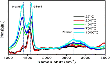 |
| | Fig. 3 Typical Raman spectra of HDLC with different annealing temperatures. | |
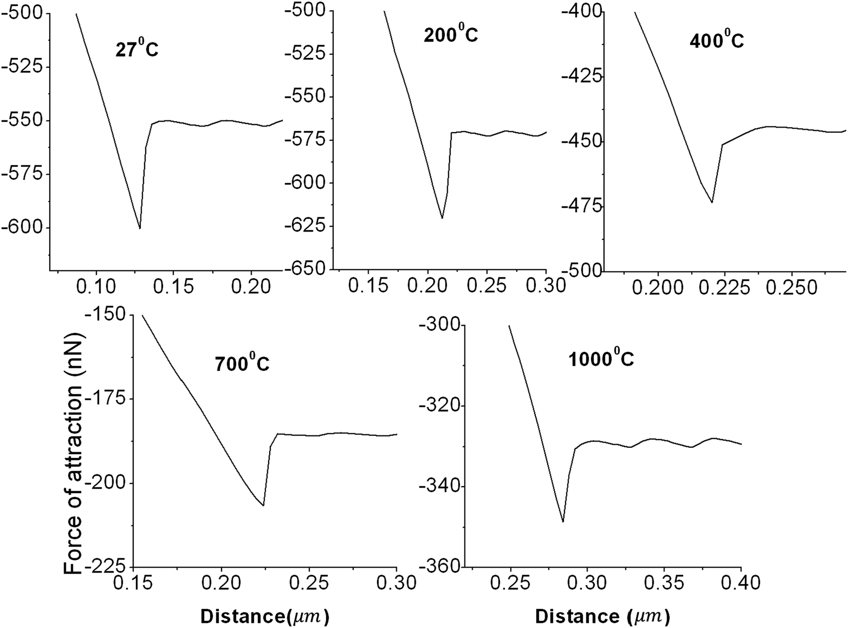
Table 1 Variation of the sp2/sp3 ratio and force of attraction with annealing temperature
| Sample |
Annealing temperature (°C) |
Force of attraction (nN) |
sp2 |
sp3 |
sp2/sp3 |
| HDLC |
27 |
50.50 |
61.33 |
38.67 |
1.58 |
| 200 |
48.80 |
63.77 |
36.22 |
1.76 |
| 400 |
28.70 |
77.96 |
22.04 |
3.54 |
| 700 |
21.20 |
83.82 |
16.18 |
5.18 |
| 1000 |
21.00 |
84.80 |
15.20 |
5.58 |
Fig. 4 presents the force of attraction vs. annealing temperature of the sample using a Si3N4 cantilever tip with a spring constant of ∼0.765 N m−1 obtained by AFM to probe the distant assigned forces between the Si3N4 and HDLC surfaces separated by air. Fig. 5 presents the distance-dependent force curves along the X-axis cantilever tip to the sample distance and along the Y-axis attraction force between the tip and sample in nanonewtons (nN). From Fig. 5, it is seen that the values of the force of attraction between HDLC and the annealed28 HDLC surfaces and silicon nitride probe decrease gradually as the annealing temperature goes from 27 °C to 1000 °C, as shown in Table 1. This gives the impression that with the decrease of bonded hydrogen, as we increase the sample temperature from 27 °C to 1000 °C, a decrease in the force of attraction between the sample and the Si3N4 tip is observed. This is caused by a decrease in the density after annealing or an increase in the electron density on the surface of the annealed sample due to graphitization, as shown in Fig. 4. This is due to the influence of the sp2/sp3 ratio29 (ID/IG), which increases with temperature, as supported by the Raman spectra.
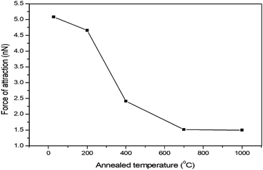 |
| | Fig. 4 Force of attraction vs. annealed temperature. | |
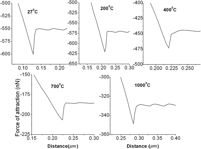 |
| | Fig. 5 Typical force vs. distance curves at different annealing temperatures of the HDLC surface using a spring constant of 0.765 N m−1 in air for the Si3N4 tip. | |
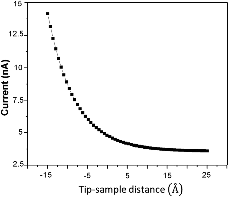
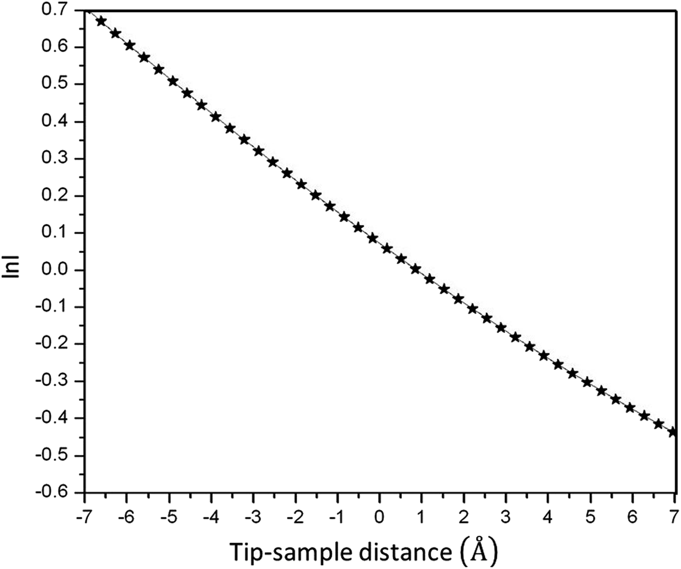
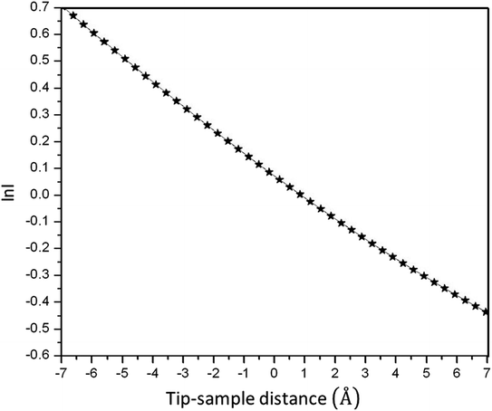
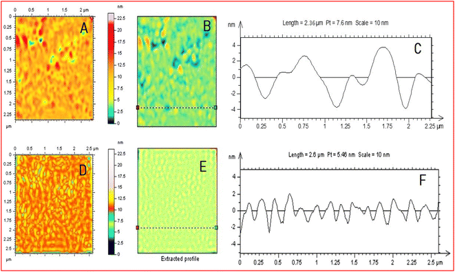
It is impossible to measure the fixed-current STM image for the as-prepared HDLC films due to their non-conductive nature, but it is possible with the annealed one due to its conductive nature, as shown in Fig. 6. Fig. 6(A) shows a non-contact-mode AFM topography image of the as-prepared HDLC surface (scan size 2.5 μm × 2.5 μm), which significantly differs from the images in Fig. 6(B)–(F), which are nanoscale STM images of the annealed HDLC films with a scan size of 60 nm × 60 nm. Fig. 7 presents a typical tunneling current vs. tip–sample distance plot and Fig. 8 presents a ln(current) vs. tip–sample distance plot for the annealed HDLC film surface. This outcome points to the usual current vs. height relation.30 The calculated work function of the annealed (400 °C) film obtained from the slope of the curve31 (Fig. 8) is ∼0.021 eV, which is about 214 times lower than the work function of a pristine graphene film (∼4.5 eV).32 Another reason for this significant change in work function can be ascribed to the preferential contact of graphene with an insulating or metallic substrate, which can alter the Fermi energy level.32,33 The conductivity and mechanical properties of annealed HDLC increase due to the increase in the number of graphene layers with the graphitization of HDLC at high temperatures.
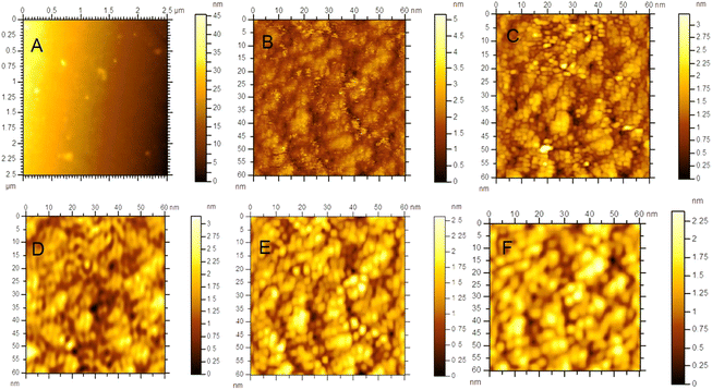 |
| | Fig. 6 (A) Non-contact-mode AFM topography image of the HDLC surface; scan size: 2.5 μm × 2.5 μm. STM images of the annealed HDLC film at (B) 200 °C, (C) 300 °C, (D) 400 °C, (E) 700 °C (F) and 1000 °C; scan size: 60 nm × 60 nm. | |
 |
| | Fig. 7 Typical tunneling current vs. distance curve for the annealed (400 °C) sample. | |
 |
| | Fig. 8 Semilogarithmic plot of the tunneling current vs. distance for the annealed (400 °C) HDLC sheet. | |
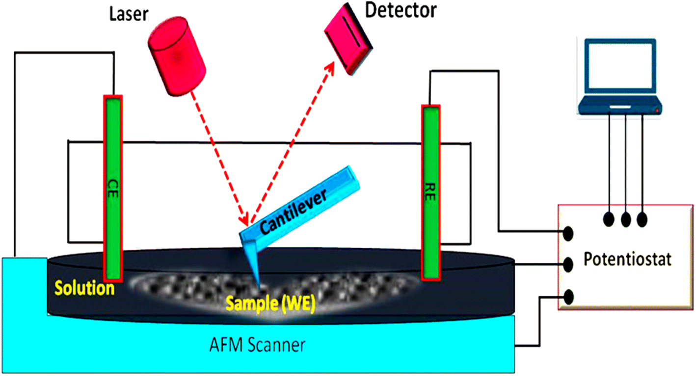
Fig. 9 presents a schematic diagram of the EC-AFM with a potentiostat. Fig. 10(A)–(C) present a non-contact-mode AFM image in the range of −1.0 to 0.0 V in the reduction process, a line of the image of HDLC along with the surface measure roughness (RMS ∼ 0.721 nm), and the corresponding height profile, while Fig. 10(D)–(F) present a non-contact-mode AFM image in the range of 0.0 to 1.0 V in the oxidation process, a line of the image of HDLC along with the surface measure roughness (RMS ∼ 0.571 nm) and corresponding height profile; both have a scan size of 2.5 μm × 2.5 μm. Fig. 10(A) and (D) significantly differ from the non-contact-mode image of HDLC in Fig. 6(A) due to the change in the surfaces by the cathodic peak potential and anodic peak potential.
 |
| | Fig. 9 Schematic drawing of the electrochemical AFM (EC-AFM) with a potentiostat. | |
 |
| | Fig. 10 (A) Non-contact-mode AFM image in the range of −1.0 V–0 V with the cathodic peak potential (B) indicated by a line in the HDLC image along the surface and (C) the corresponding height profile. (D) Non-contact mode AFM image in the range of 0 V–1.0 V with the anodic peak potential (E) indicated by a line in the HDLC image along the surface and (F) the corresponding height profile. Scan size: 2.5 μm × 2.5 μm. | |
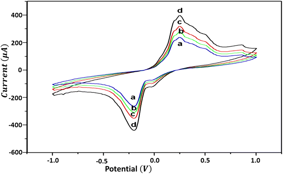
Fig. 11 presents the cyclic voltammograms with different scan rates. The peak potential of the working electrode is +0.216 V during a forward-biased scan from negative to positive (−1.0 to +1.0 V), which is referred to as the anodic peak potential Epa. Similarly, the peak potential of the working electrode is −0.210 V during a reverse-biased scan from positive to negative (+1.0 to −1.0 V), which is referred to as the cathodic peak potential Epc. The separation of peak potentials (ΔE = Epa − Epc) is 426 mV, which is considerably large, indicating a quasi-reversible biased behavior of the working electrode (HDLC surface) at a scan rate range of 50 mV s−1 to 200 mV s−1.34 This indicates that the HDLC film surface after irreversibly undergoing a surface redox couple reaction can donate and receive electrons owing to the presence of sp2 CC (donor) and sp3 C–H (acceptor) carbons present homogenously in the HDLC film with a thickness of ∼168 nm.35 The quasi-reversible process on the HDLC film suggests that during the reduction of HDLC, the effect is finite unless we provide an external potential to remedy oxidation, which means that more hydrogen can be stored in this process.
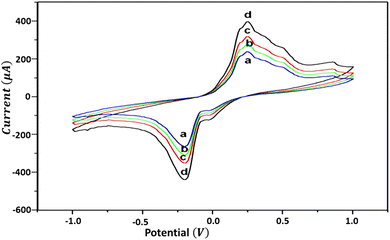 |
| | Fig. 11 Cyclic voltammograms of the HDLC electrode at various scan rates: (a) 50 mV s−1, (b) 100 mV s−1, (c) 150 mV s−1 and (d) 200 mV s−1. The electrolyte is 1 mM K3Fe(CN)6/0.1 M H2SO4. | |
Electrodes that tend to be hydrophobic, such as diamond, HDLC, and other carbon-based electrodes, can promote hydrophobic interactions with hydrophobic analytic species, such as proteins and aromatic compounds, and foul the electrode.36 Due to the chemical inertness and wide potential window of our HDLC film, it shows reproducible electron transfer and behaves as a quasi-reversible working electrode in the presence of a hydrophilic electrolyte. The I–V characteristic behavior presents a wide potential window, and HDLC exhibits ambipolar behavior; the top view from the schematic drawing of HDLC surface37 shows the coherent domains of sp3 C–H (non-conducting) and sp2 CC (conducting) carbons. This indicates the resistive nature of the HDLC surface, which has been previously discussed.37 Hydrogenated diamond-like carbon (HDLC) is a promising electrode material owing to its unique electrochemical properties, such as chemical inertness, resulting in a wide potential window and low background current. The basic electrochemical properties and responses of HDLC to several redox systems have also been investigated and recently reviewed. One of the main factors that determines the properties of a given HDLC material is the ratio of sp3 to sp2 bonded carbon in the film.
4. Conclusions
We have synthesized an HDLC thin-film via chemical vapor deposition. As the materials are synthesized from a gaseous system using radio frequency plasma (RF plasma), they did not require high heat and pressure. Hence, this method is cost-effective. The thermal annealing effect on the properties of the obtained HDLC thin-films has been studied by preferentially synthesizing the films on silicon (100) substrates using the plasma-enhanced chemical vapor deposition technique. The structural, electrical, and hybridization (sp2/sp3) calculations of the as-deposited and annealed films were determined to investigate these effects. An appreciable reduction in the hydrogen concentration upon annealing of the samples was predicted using FTIR spectroscopy, which is supported by Raman spectroscopy. AFM, STM, and EC-AFM studies were performed to measure the transformation in the HDLC thin-films by annealing. Using Raman, STM, and EC-AFM analyses, the nature of the conductivity and functionality of the surface were determined. In conclusion, the application of the scanning probe measurement technique is highly effective and may be successfully used to characterize HDLC, graphene or graphite-like carbon materials, as has been demonstrated above.
Author contributions
Hari Shankar Biswas: resources, conceptualization, investigation, formal analysis, validation, writing – review & editing; Jagannath Datta: investigation, formal analysis, writing; Prasenjit Mandal: writing – review & editing; Sandeep Poddar: formal analysis, writing – review & editing, validation; Amit Kumar Kundu: writing – review & editing; Indranil Saha: validation; proof checking, grammar correction.
Conflicts of interest
There are no conflicts to declare.
Acknowledgements
One of the authors (Hari Shankar Biswas) thanks the UGC Minor Project, Reference No. F.PSW-140/15-16, for funding. The authors also thank Dr Susanta Debnath, Saha Institute of Nuclear Physics, Mr U.S. Sil of PPD, SINP, Dr Suchandra Chatterjee, and Dr Lalita Das, Department of Chemistry, Surendranath College, for the characterization of the samples and their technical help during the experiments in this work.
References
- S. Aisenberg and R. Chobat, J. Appl. Phys., 1971, 42, 2935 CrossRef.
- H. S. Biswas, J. Indian Chem. Soc., 2019, 96, 413–418 Search PubMed.
- W. S. Choi, K. Kim, J. Yi and B. Hong, Mater. Lett., 2008, 62, 577 CrossRef CAS.
- Z. Panosyan, Thin Solid Films, 2009, 517, 5404 CrossRef CAS.
- M. I. Landstrass and K. V. Ravi, Appl. Phys. Lett., 1989, 55(10), 975 CrossRef CAS.
- W. Zhang, J. Einstein and L. Ley, Phys. Rev. E: Stat., Nonlinear, Soft Matter Phys., 2008, 78(4), 041603 CrossRef PubMed.
- W. Choi and B. Hong, Renewable Energy, 2008, 33, 226 CrossRef CAS.
- H. Li, X. Tao, C. Wang, C. Jianmin, H. Zhou and H. Liu, Thin Solid Films, 2006, 515, 2153–2160 CrossRef CAS.
- K. Taube, Surf. Coat. Technol., 1998, 98, 976 CrossRef CAS.
- J. L. Dividson, W. P. Kang, Y. Gurbuz, K. C. Holmes, L. G. Davis, A. Wisitora-at, D. V. Kerns, R. L. Eidson and T. Henerson, Diamond Relat. Mater., 1999, 8, 1741 CrossRef.
- G. Dearnaley, Clin. Mater., 1993, 12, 237–244 CrossRef CAS PubMed.
- S. Ravi and P. Silva, EMIS Datareviews series EMIS Processing Series, ed. B. Weiss, INSPEC, The Institution of Electrical Engineers, London, United Kingdom, 2003 Search PubMed.
- F. Airoldi, A. Colombo, D. Tavano, G. Stankovic, S. Klugmann and V. Paolillo, et al., Am. J. Cardiol., 2004, 93, 474–477 CrossRef CAS PubMed.
- H. S. Tran, M. M. Puc, C. W. Hewitt, D. B. Soll, S. W. Marra and V. A. Simonetti, et al., J. Invest. Surg., 1999, 12, 133–140 CrossRef CAS PubMed.
- J. K. Luo, J. H. He, Y. Q. Fu, A. J. Flewitt, N. A. Fleck and W. I. Milne, J. Micromech. Microeng., 2005, 15, 1406 CrossRef CAS.
- J. Zhang, F. Zhang, H. Yang, X. Huang, H. Liu, J. Zhang and S. Guo, Langmuir, 2010, 26(9), 6083–6085 CrossRef CAS PubMed.
- S. Fenghua, C. Guofu and J. Sun, Tribol. Int., 2019, 130, 1–8 CrossRef.
- H. S. Biswas, J. Datta, D. P. Chowdhury, A. V. R. Reddy, U. C. Ghosh, A. K. Srivastava and N. R. Ray, Langmuir, 2010, 26(22), 17413–17418 CrossRef CAS PubMed.
- M. R. Roy, E. Pascual and M. C. Polo, Surf. Coat. Technol., 2008, 202, 2354 CrossRef.
- R. Paul, S. Dalui, S. N. Das, R. Bhar and A. K. Pal, Appl. Surf. Sci., 2008, 255, 1705 CrossRef CAS.
- R. Wächter and A. Cordery, Diamond Relat. Mater., 1999, 8, 504 CrossRef.
- A. M. M Omer, S. Adhikari, S. Adhikary, M. Rusop, H. Uchida, T. Soga and M. Umeno, Diamond Relat. Mater., 2006, 15, 645 CrossRef.
- H. Weidong, D. Ding and Z. Rujuan, Plasma Sci. Technol., 2004, 6, 2255 CrossRef.
- J. Datta, H. S. Biswas, P. Rao, G. L. N. Reddy, S. Kumar, N. R. Ray, D. P. Chowdhury and A. V. R. Reddy, Nucl. Instrum. Methods Phys. Res., Sect. B, 2014, 328, 27–32 CrossRef CAS.
- E. Titusa, D. S. Misra and A. K. Sikder, Diamond Relat. Mater., 2005, 14, 476 CrossRef.
- E. F. Sheka, Y. A. Golubev and N. A. Popova, Nanomaterials, 2020, 10, 2021 CrossRef CAS PubMed.
- A. Singha, A. Ghosh, A. Roy and N. R. Ray, J. Appl. Phys., 2006, 100(8), 44910 CrossRef.
- C. Casiraghi, A. C. Ferrari and J. Robertson, Phys. Rev. B: Condens. Matter Mater. Phys., 2005, 72(14), 85401 CrossRef.
- Z. Lu, B. Zhang, N. Yao, X. Zhang, B. Ma and Z. Fan, IEEE Cat., 2004, 04EX839 Search PubMed.
- N. Noei, A. Weismann and R. Berndt, Beilstein J. Nanotechnol., 2018, 9, 3048–3052 CrossRef CAS PubMed.
- https://www.ntmdt.com/spm-basics/view/current-distance-characteristic.
- Y. J. Yu, Y. Zhao, S. Ryu, L. E. Brau, K. S. Kim and P. Kim, Nano Lett., 2009, 9(10), 3430–3434 CrossRef CAS PubMed.
- G. Giovannetti, P. A. Khomyakov, G. Brocks, V. M. Karpan, J. van den Brink and P. J. Kelly, Phys. Rev. Lett., 2008, 101, 026803 CrossRef CAS PubMed.
- A. J. Bard and L. R. Faulker, Electrochemical methods: fundamentals and applications, John Wiley & Sons Inc., New York, 2nd edn, 2001, vol. 239, ch. 6, ISBN: 978-0-471-04372-0 Search PubMed.
- J. Datta, N. R. Ray, P. Sen, H. S. Biswas and E. A. Vogler, Mater. Lett., 2012, 71, 131 CrossRef CAS.
- L. H. Benjamin, S. Shajahan and D. K. Y. Wong, Rev. Anal. Chem., 2016, 35(1), 1–28 Search PubMed.
- H. S. Biswas, Int. J. Adv. Res. Sci. Eng. Technol., 2018, 9(5), 87–94 Search PubMed.
|
| This journal is © The Royal Society of Chemistry 2022 |
Click here to see how this site uses Cookies. View our privacy policy here. 
 Open Access Article
 This Open Access Article is licensed under a Creative Commons Attribution-Non Commercial 3.0 Unported Licence
 *a,
Jagannath Dattab,
Prasenjit Mandalc,
Sandeep Poddar
*a,
Jagannath Dattab,
Prasenjit Mandalc,
Sandeep Poddar