
 Open Access Article
 This Open Access Article is licensed under a
 Creative Commons Attribution 3.0 Unported Licence
Ultra-low detection limit chemoresistive NO2 gas sensor using single transferred MoS2 flake: an advanced nanofabrication†
Hoang Si Hong*a,
Tran Vinh Hoang b,
Nguyen Thanh Huonga,
Nguyen Hoang Nama,
Dao Duc Thinha,
Nguyen Thi Huea and
Nguyen Duc Thuana
b,
Nguyen Thanh Huonga,
Nguyen Hoang Nama,
Dao Duc Thinha,
Nguyen Thi Huea and
Nguyen Duc Thuana
aSchool of Electrical and Electronic Engineering, Hanoi University of Science and Technology (HUST), No. 1 Dai Co Viet Road, Hanoi, Vietnam. E-mail: hong.hoangsy@hust.edu.vn; Tel: +84-43-869-6211
bSchool of Chemical Engineering, Hanoi University of Science and Technology (HUST), No. 1 Dai Co Viet Road, Hanoi, Vietnam
First published on 22nd November 2022
Abstract
In this work, a method of fabricating a NO2 nano-sensor working at room temperature with a low detectable concentration limit is proposed. A 2D-MoS2 flake is isolated by transferring a single MoS2 flake to SiO2/Si substrate, followed by applying an advanced e-beam lithography (EBL) to form a metal contact with Au/Cr electrodes. The resulting chemoresistive nano-sensor using a single MoS2 flake was applied to detect a very low concentration of NO2 at the part-per-billion (ppb) level. This result is obtained due to the ability to create microscopic nano-sized MoS2 gaps using e-beam lithography (300 nm–400 nm). Experimental results also show that the sensor can capture changes in concentration and send the information out extremely quickly. The response and recovery time of the sensor also reached the lowest point of 50 and 75 ms, outperforming other sensors with a similar concentration working range.
1. Introduction
The amount of poisonous gases emitted into the environment has significantly increased due to industrial development as well as improvements in quality of life and transit accessibility, causing substantial harm to the ecosystem and the general public, making it necessary to monitor the air quality in metropolitan areas.1,2 Among the aforementioned air contaminants, NO2 is one of the most deadly as at concentrations over 1 ppm, it causes or aggravates respiratory disorders including emphysema and bronchitis as well as severe damage to lung tissues in humans.3 Therefore, research on gas sensors is helpful for the NO2 emission monitoring and controlling process and is a potential research direction where a large number of scientists are currently interested.Two-dimensional (2D) materials have been applied in various research applications and industries because of their potential in chemical gas sensing, electronics, optoelectronics, optics, and energy generation.4–7 In previous works, the resistive NO2 gas sensor was fabricated using 2D materials (molybdenum disulfide MoS2/graphene hybrid), which showed high sensitivity, good selectivity, and a low detection limit.8 However, the concentration limit of that type of sensor is still relatively high and is not suitable for monitoring NO2 in the surrounding environment. The nano-sensor deployed by the combination of two-dimensional (2D) materials of atomic-layer thickness and the advantages of nanofabrication is an urgent research direction because of excellent outcomes in the chemical gas sensing field. However, the biggest challenge in this research direction is how we can make sensor devices at the nanoscale to quickly trap these changes in 2D materials, i.e., what is the optimal design and what are the proper materials. This has been the motivation for us to conduct experiments to fabricate a highly sensitive nanoscale NO2 gas sensor using advanced materials.
MoS2 has recently been suggested as a promising material for NO2 gas sensing9–12 because, when combined with graphene to create composite or hybrid materials, it increases sensitivity due to synergistic effects and eliminates the issue of high recovery time of graphene-only NO2 sensor.13 Moreover, the challenge in developing chemoresistive sensors is the distance between electrodes, which is limited by e-beam lithography technology. The short distance between electrodes and the sensing area at truly nanoscale give such advantages as fast response and low detection limit.14 In this work, we transferred a single MoS2 flake to SiO2/Si and applied advanced e-beam lithography to make chemoresistive nanosensors to detect a very low concentration of NO2 gas.
2. Experimental section
2.1 Transferred MoS2 and fabrication of chemoresistive nanosensor
As previously mentioned,8 MoS2 was deposited together with the CVD-based synthesis of graphene utilizing copper foil and transferred to SiO2/Si. To fabricate a chemoresistive NO2 gas sensor, two steps of e-beam lithography were applied. In the first step, the array of Au/Cr marker was fabricated on SiO2/Si using 100 nm thick PMMA as e-beam resist. Then, the single MoS2 flake was transferred to SiO2/Si (with Au/Cr marker on top) using 3M Scotch tape. The intermediate SEM observation step is to find the MoS2 flake on SiO2/Si after the transferring process and identify the MoS2 flake position using Au/Cr marker. After identifying the MoS2 flake location on the array Au/Cr marker with high precision, the second e-beam step was performed on PMMA (100 nm)/MoS2/SiO2/Si to make metal contact by the lift-off process. Then, two Au/Cr electrodes were deposited on MoS2/SiO2/Si by e-beam evaporation to make the final chemoresistive nano-sensor device. The illustration of chemoresistive NO2 nanosensor fabrication process is shown in Fig. 1.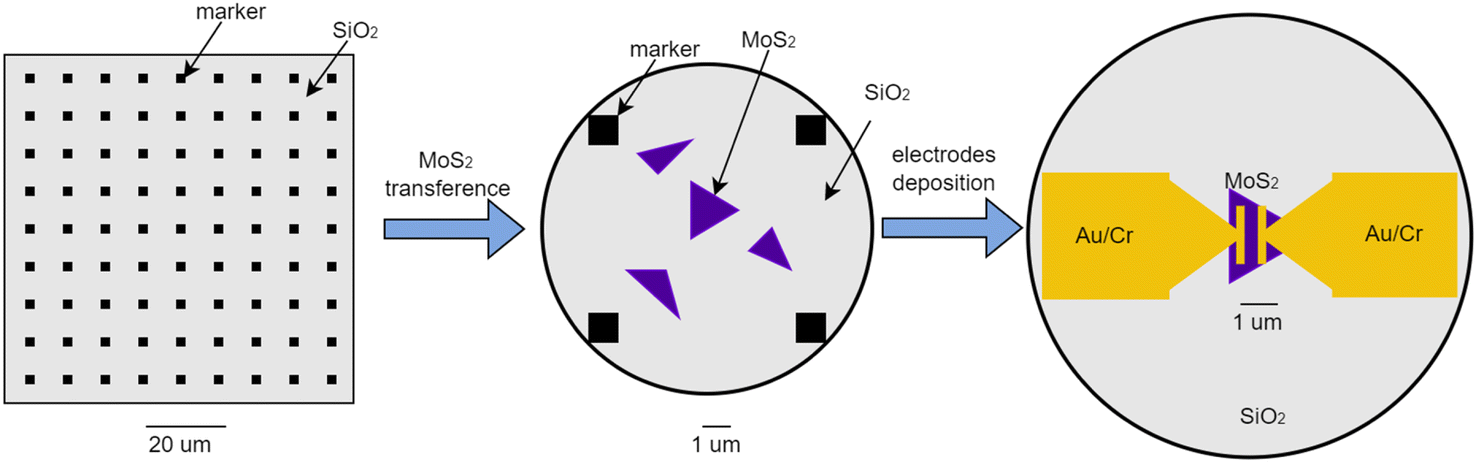 | ||
| Fig. 1 The illustration of the chemoresistive NO2 nanosensor fabrication process. | ||
2.2 Evaluation methods
The morphology and nanofabrication of the MoS2/SiO2/Si sample were determined using high-resolution scanning electron microscopy (HR-SEM; SU 8010, Hitachi) and high-resolution e-beam lithography (e-Raith 150). High-resolution transmission electron microscopy (HR-TEM; JEM-2100F, JEOL) was used to gauge the atomic structure and thickness of transferred MoS2. Raman spectroscopic measurements were conducted in WITec Raman imaging with a 532 nm laser source to identify MoS2 quality before/after the transferring process. The NO2 gas sensor was installed inside a sealed chamber that was attached to NO2 gas cylinders with various concentrations. The I–V characteristics and resistance of the sensor were recorded using a semiconductor probe station (Keithley SCS-4200). The detailed measurement setup for the NO2 gas sensor was described in previous work.83. Results and discussion
As-grown MoS2–graphene hybrid and a single MoS2 flake on SiO2/Si after the transfer process are depicted in SEM images in Fig. 2(a). It is obvious that the MoS2 with 2D crystallite was grown on graphene and was triangle-shaped. The triangle-like MoS2 flakes are with average sizes of around 1–2 μm. The MoS2 flakes were grown in a large-scale area on graphene with uniform thickness as shown in AFM images in Fig. 2(b). In Fig. 2(c), the transferred MoS2 seems to induce defects during the transfer process by breaking into smaller flakes compared with the original MoS2 flake as-deposited on graphene (see AFM image in Fig. 2(b)). In order to measure the thickness of MoS2 flakes on graphene, the AFM with tapping mode was carried out. Results in MoS2 flake average thickness is around 5 nm, according to 10 layers of MoS2, consistent with the report in ref. 8. Fig. 2(d) shows the cross-sectional view of HR-TEM of transferred MoS2 on SiO2/Si substrate, which indicates 8 layers of MoS2.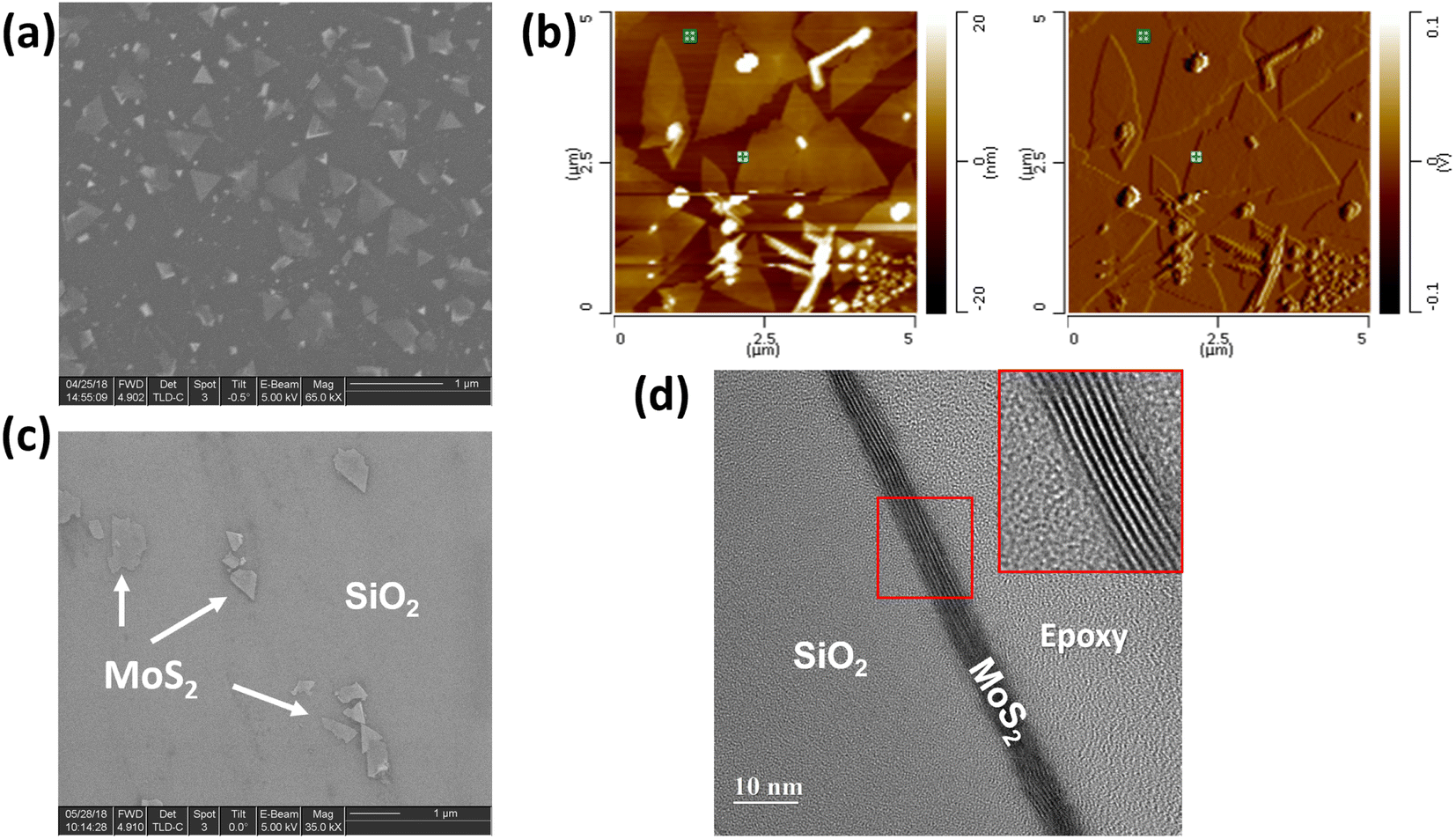 | ||
| Fig. 2 MoS2 flakes deposited on graphene: (a) SEM image, (b) AFM analysis, (c) SEM images of isolated MoS2 flake on SiO2/Si after the transferring process and (d) cross-sectional view of HR-TEM analysis of transferred MoS2 on SiO2/Si (with the help of focused-ion-beam (FIB) to prepare sample specimen). | ||
Fig. 3 shows the Raman spectra of a few layers of MoS2 growth on graphene and their Raman mapping. In Fig. 3(a), two Raman peaks were assigned to MoS2 material (Eg at ∼378.5 cm−1 and A1g at ∼405.8 cm−1).8 The Eg modes are doubly degenerate in-plane vibrational modes and A1g is an out-of-plane vibration mode, which agrees well with previous observations in β-phase bulk MoS2.15 In comparison with the Raman spectrum of transferred pure MoS2 flakes (transferring from MoS2/graphene/SiO2/Si sample) on SiO2/Si substrate, both peak frequencies of β-phase (Eg and A1g) of MoS2–graphene shift to the higher wavenumber region. The Raman peaks of transferred MoS2 flakes on SiO2/Si, as shown in Fig. S1,† are at 370.9 and 401.2 cm−1 for Eg and A1g mode, respectively. The shift in Raman peaks of MoS2 material is due to either a strain/stress free state after transferring from graphene or the influence of the thickness of a few-layers MoS2 on Raman shift.15 The G and 2D bands of graphene were assigned to two minor peaks at 1584.3 cm−1 and 2677.2 cm−1, respectively. The in-plane vibration of sp2-carbon atoms was attributed to the G band, while defects in graphene were associated with the D band's breathing modes of six-atom rings. The D band, which is at around 1350 cm−1 indicating defects in graphene, was not present in the sample after depositing MoS2 as in Fig. 3(a). However, the 2D peaks indicating the number of layers of graphene or graphene quality appeared at 2677.2 cm−1. The intensities of graphene-related peaks are lower than MoS2 peaks because of either the thickness of the few-layer MoS2 or the focus point of the laser from Raman. Fig. 3(b) shows an optical image of MoS2–graphene and the selected area for Raman mapping. Fig. 3(c and d) are images for Raman mapping for average peak intensity centered at 405.8 cm−1 and 378.5 cm−1 for A1g and Eg mode of MoS2 material, respectively. The A1g peak has clear contrast on the area of MoS2 flakes in comparison with the Eg peak, which indicated the higher intensity of A1g mode in MoS2 flakes. Fig. 3(e and f) are images of Raman mapping of G and 2D peaks related to graphene, respectively. In conversion, the mapping of peaks related to graphene has more uniformity in color, except at the graphene grain boundary, which gives higher intensity in Fig. 3(e and f) due to the thicker thickness of folded graphene at the boundary. These Raman mapping images confirm the MoS2 as isolated flakes on the base planar graphene layer.
 | ||
| Fig. 3 (a) Raman spectra of MoS2–graphene on SiO2/Si and (b) optical image with selected area for Raman mapping, (c) Raman mapping for A1g mode, (d) Raman mapping for Eg mode of MoS2, Raman mapping for (e) G peak and (f) 2D peak of graphene. | ||
Fig. 4(a) shows the fabricated chemoresistive sensor using a single transferred MoS2 flake. The Au/Cr metal contact on a single MoS2 flake is with a distance of 300 nm between two electrodes. The fabricated sensor was tested several times during the day and on different days. Results showed a consistent response with the same testing conditions (NO2 gas concentrations and bias voltage). Fig. 4(b–d) shows the sensor responses with a low concentration of NO2 gas. The I–V curves were recorded with synthetic air and different NO2 gas concentrations of 1, 10, and 100 ppb as shown in Fig. 4(b). The fabricated sensor showed a clearly different response with various NO2 concentrations. Fig. 4(b) indicates the maximum response of the fabricated sensor with 100 ppb NO2. I–V curves in Fig. 4(b) show that the sensor response increased dramatically in the forwarding region when exposed to NO2 gas. The non-linear behavior in the I–V characteristic of Au/MoS2/Au sample is due to either space-charge limited current in 2D materials16 or oxidized MoS2 surface giving the nano-junction with Au electrode. With the same sample structure without MoS2 flakes, pure graphene sample (with two Au/Cr electrodes and a distance of 300 nm) shows linear ohmic contact and negligible change when exposed to 100 ppb NO2 gas (see Fig. S2 in ESI†). Fig. 4(c) shows the transient response of the fabricated sensor with 5 V bias exposed under 3 repeat cycles of 1, 10, and 100 ppb. The sensor response shows good repeatability and the gas-induced-current increased by two orders of its value when exposed to NO2 gas. The response/recovery time of the fabricated sensor is estimated at around 50/75 ms. Fig. 4(d) shows the transient response to 3 cycles of 100 ppb NO2 at a lower bias voltage of 1 V. The current increased only 4-fold with 100 ppb NO2 at 1 V bias, which is much smaller than with a 5 V bias. The NO2 gas generated more current in Au–MoS2–Au at a higher bias voltage in comparison with a low bias voltage due to the influence of the external electrical field on electron–hole separation and charge collection at the electrode.14,16 The performance of the fabricated NO2 gas sensor can be compared with previously developed sensors (Table 1).17–21 All of them are sensors that work at NO2 concentrations at ppb, so all comparisons are fair. It is evident that the proposed sensor exhibited a low limit of detection and high sensitivity, among others. In addition, the response/recovery time of the proposed sensor also outperforms others by being more than 60 times faster. In Table 1, the sensor response (S) at fixed bias voltage is defined as the ratio of current change when the sensor is exposed to NO2:
| S = Ig/Ia | (1) |
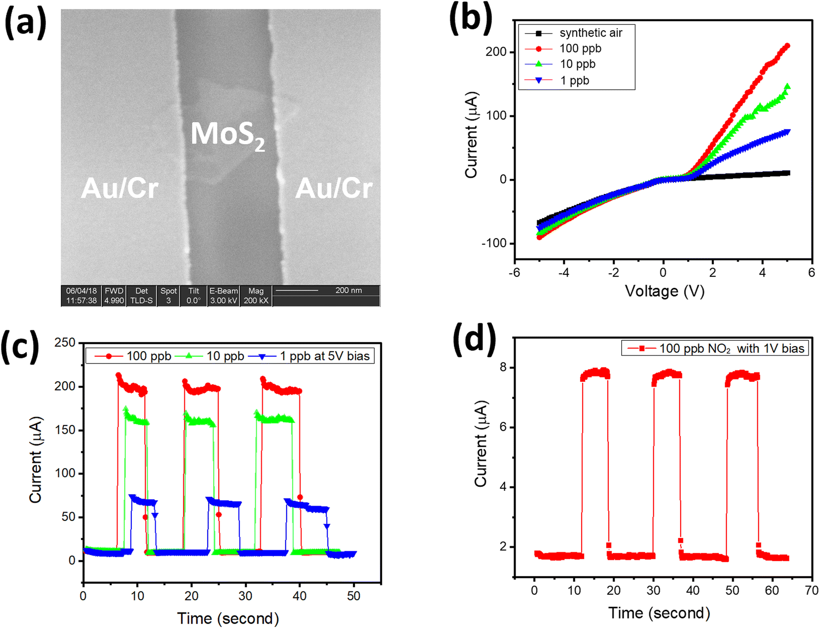 | ||
| Fig. 4 (a) SEM image of the fabricated nanosensor of Au–MoS2–Au, (b) I–V characteristics of sensors with various NO2 concentrations, (c) repeatability response of sensor with different NO2 concentrations of 1, 10, 100 ppb at 5 V bias (d) transient response to 3 cycles of 100 ppb at 1 V bias. | ||
| Materials | Experimental detected concentration (ppb) | Sensor response (S = Ig/Ia) | Response/recovery time | Condition | Ref. |
|---|---|---|---|---|---|
| ZnO | 25 | 0.16 | — | 100 °C UV light | 17 |
| ZnO | 25 | 1.65 | — | RT UV light | 18 |
| Cu2O–CuO microflowers-2 | 10 | 1.6 | 75 s/100 s | 187 °C 30% RH | 19 |
| SnS2 nanopetals | 5 | 19.7 | 179 s/782 s | RT | 20 |
| CuO nanoflakes/rGO | 50 | 20.6 | 31.8 s/60.6 s | RT | 21 |
| MoS2/SiO2 | 1 | 5.1 | 50 ms/75 ms | RT | This work |
| MoS2/SiO2 | 10 | 12.9 | 50 ms/75 ms | RT | This work |
The sensor response of pure graphene with NO2 is shown in Fig. S2(b and c).† Obviously, the Au–MoS2–Au showed significantly higher responsivity in comparison with pure graphene (for responsivity of pure graphene, see Fig. S1 in ESI†). The sensor made of Au–MoS2–Au has increased responsivity from 4 to 100 with 100 ppb NO2 at 1 V and 5 V bias, respectively. Meanwhile, the sensor response of pure graphene is not significant, which is less than 1% in Fig. S2(b and c),† at 1 V and 5 V bias. The selectivity of the fabricated sensor towards NO2, in comparison with common toxic gases/moisture such as H2, H2O, CO, and CO2, is shown in Fig. S2(d).† In Fig. S2(d),† examined gases/moisture were measured at 1000 ppb, and the negative sensor response indicates that the current was reduced with H2, CO, and CO2 gas. Results showed good selectivity of the fabricated sensor towards NO2 gas, which is promising for practical applications.
4. Conclusions
In this work, MoS2 was successfully deposited on graphene by thermal CVD. The single MoS2 flake was then transferred successfully to SiO2/Si substrate as isolated flakes. Advanced e-beam lithography was applied to fabricate the nanosensor with a single MoS2 flake only. The created nanosensor could identify low NO2 concentrations between 1 and 100 ppb at room temperature, showing a fast response/recovery of 50/75 ms. Thanks to the recent advantages of nanofabrication in combination with the development of 2D materials, the chemical gas sensor at truly nanoscale showed its advantages with low detection limit and fast response and is promising for detecting NO2 at the atomic level in practical applications. In future works, the performance of the fabricated sensor will be considered over a long-term period.Conflicts of interest
There are no conflicts to declare.Acknowledgements
This research is funded by the Vietnam National Foundation for Science and Technology Development (NAFOSTED) under grant number 103.02-2018.33.References
- G. F. Fine, L. M. Cavanagh, A. Afonja and R. Binions, Metal oxide semi-conductor gas sensors in environmental monitoring, Sensors, 2010, 10, 5469–5502 CrossRef CAS
.
- K. Wetchakun, T. Samerjai, N. Tamaekong, C. Liewhiran, C. Siriwong, V. Kruefu, A. Wisitsoraat, A. Tuantranont and S. Phanichphant, Semiconducting metal oxides as sensors for environmentally hazardous gases, Sens. Actuators, B, 2011, 160, 580–591 CrossRef CAS
- S. Novikov, N. Lebedeva, A. Satrapinski, J. Walden, V. Davydov and A. Lebedev, Graphene based sensor for environmental monitoring of NO2, Sens. Actuators, B, 2016, 236, 1054–1060, DOI:10.1016/j.snb.2016.05.114
- N. Yamazoe and N. Miura, Environmental gas sensing, Sens. Actuators, B, 1994, 20, 95–102 CrossRef CAS
- L. Duk-Dong and L. Dae-Sik, Environmental gas sensors, IEEE Sens. J., 2001, 1, 214–224 Search PubMed
- S. Liu, M. Wang, G. Liu, N. Wan, C. Ge, S. Hussain, H. Meng, M. Wang and G. Qiao, Enhanced NO2 gas-sensing performance of 2D Ti3C2/TiO2 nanocomposites by in-situ formation of Schottky barrier, Appl. Surf. Sci., 2021, 567, 150747 CrossRef CAS
- M. Cheng, Z. Wu, G. Liu, L. Zhao, Y. Gao, B. Zhang, F. Liu, X. Yan, X. Liang, P. Sun and G. Lu, Highly sensitive sensors based on quasi-2D rGO/SnS2 hybrid for rapid detection of NO2 gas, Sens. Actuators, B, 2019, 291, 216–225 CrossRef CAS
- H. S. Hong, N. H. Phuong, N. T. Huong, N. H. Nam and N. T. Hue, Highly sensitive and low detection limit of resistive NO2 gas sensor based on a MoS2/graphene two-dimensional heterostructures, Appl. Surf. Sci., 2019, 492, 449–454 CrossRef CAS
- J. Guo, R. Wen, J. Zhai and Z. L. Wang, Enhanced NO2 gas sensing of a single-layer MoS2 by photogating and piezo-phototronic effects, Sci. Bull., 2019, 64, 128–135 CrossRef CAS
- N. Yi, Z. Cheng, H. Li, L. Yang, J. Zhu, X. Zheng, Y. Chen, Z. Liu, H. Zhu and H. Cheng, Stretchable, ultrasensitive, and low-temperature NO2 sensors based on MoS2@rGO nanocomposites, Mater. Today Phys., 2020, 15, 100265 CrossRef
- W. Li, M. Shahbazi, K. Xing, T. Tesfamichael, N. Motta and D.-C. Qi, Highly Sensitive NO2 Gas Sensors Based on MoS2@MoO3 Magnetic Heterostructure, Nanomaterials, 2022, 12, 1303 CrossRef CAS PubMed
- R. Kumar, P. K. Kulriya, M. Mishra, F. Singh, G. Gupta and M. Kumar, Highly selective and reversible NO2 gas sensor using vertically aligned MoS2 flake networks, Nanotechnology, 2018, 29, 464001 CrossRef
- S. Novikov, N. Lebedeva, A. Satrapinski, J. Walden, V. Davydov and A. Lebedev, Graphene based sensor for environmental monitoring of NO2, Sens. Actuators, B, 2016, 236, 1054–1060 CrossRef CAS
- Y. Fujimoto and S. Saito, Gas adsorption, energetics and electronic properties of boron- and nitrogen-doped bilayer graphenes, Chem. Phys., 2016, 478, 55–61 CrossRef CAS
- H. Li, Z. Yin, Q. He, H. Li, X. Huang, G. Lu and et al, ., Fabrication of Single- and Multilayer MoS2 Film-Based Field-Effect Transistors for Sensing NO at Room Temperature, Small, 2012, 8, 63–67 CrossRef CAS
- J. Sun, N. Lin, H. Ren, C. Tang, L. Yang and X. Zhao, Gas adsorption on MoS2/WS2 in-plane heterojunctions and the I–V response: a first principles study, RSC Adv., 2016, 6, 17494–17503, 10.1039/C5RA24592C
- A. Aziz, N. Tiwale, S. A. Hodge, S. J. Attwood, G. Divitini and M. E. Welland, Core–Shell Electrospun Polycrystalline ZnO Nanofibers for Ultra-Sensitive NO2 Gas Sensing, ACS Appl. Mater. Interfaces, 2018, 10, 43817–43823, DOI:10.1021/acsami.8b17149
- G. Li, H. Zhang, L. Meng, Z. Sun, Z. Chen, X. Huang and Y. Qin, Adjustment of oxygen vacancy states in ZnO and its application in ppb-level NO2 gas sensor, Sci. Bull., 2020, 65, 1650–1658, DOI:10.1016/j.scib.2020.05.027
- N. Wang, W. Tao, X. Gong, L. Zhao, T. Wang, L. Zhao, F. Liu, X. Liu, P. Sun and G. Lu, Highly sensitive and selective NO2 gas sensor fabricated from Cu2O-CuO microflowers, Sens. Actuators, B, 2022, 362, 131803, DOI:10.1016/j.snb.2022.131803
- Y. Li, M. Dai, J. Bai, Y. Wang, Y. Li, C. Wang, F. Liu, P. Sun, T. Wang and G. Lu, Ppb-level NO2 sensing properties at room temperature of ultra-thin SnS2 nanopetals annealed at different temperatures, Sens. Actuators, B, 2022, 370, 132398, DOI:10.1016/j.snb.2022.132398
- H. Bai, H. Guo, J. Wang, Y. Dong, B. Liu, Z. Xie, F. Guo, D. Chen, R. Zhang and Y. Zheng, A room-temperature NO2 gas sensor based on CuO nanoflakes modified with rGO nanosheets, Sens. Actuators, B, 2021, 337, 129783, DOI:10.1016/j.snb.2021.129783
Footnote |
| † Electronic supplementary information (ESI) available. See DOI: https://doi.org/10.1039/d2ra06228c |
| This journal is © The Royal Society of Chemistry 2022 |