 Open Access Article
Creative Commons Attribution 3.0 Unported Licence
First principles prediction of electronic, mechanical, transport and optical properties of the silicane/Ga2SSe heterostructure
Khang D. Pham *
*
Institute of Applied Technology, Thu Dau Mot University, Binh Duong Province, Vietnam. E-mail: phamdinhkhang@tdmu.edu.vn
First published on 8th November 2022
Abstract
In this work, we investigated the electronic structure, and mechanical, transport and optical properties of the van der Waals heterostructure formed from silicane (SiH) and Janus Ga2SSe monolayers using first-principles prediction. The out-of-plane symmetry in the Janus Ga2SSe monolayer leads to the formation of two different types of Ga2SSe/SiH heterostructure, namely SGa2Se/SiH and SeGa2S/SiH stacking patterns. All stacking patterns of the SiH/Ga2SSe heterostructure are thermodynamically, mechanically and energetically stable at room temperature. Furthermore, the generation of the SiH/Ga2SSe heterostructure gives rise to a reduction in the band gap, demonstrating that the electrons move faster from the valence bands to the conduction bands. The SiH/Ga2SSe heterostructure is a semiconductor with a direct band gap of about 0.68 or 0.95 eV, depending on the stacking pattern. The SiH/Ga2SSe heterostructure forms type-II band alignment for all stacking patterns, indicating that the photogenerated carriers are separated effectively, thus enhancing the photocatalytic performance. Moreover, the carrier mobilities for electrons and holes of the Ga2SSe/SiH heterostructure are higher than those of the constituent SiH and Ga2SSe monolayers in both the x and y directions, suggesting that the performances of electronic devices based on the Ga2SSe/SiH heterostructure would be excellent and reliable. The formation of the Ga2SSe/SiH heterostructure also gives rise to an enhancement of the absorption coefficient in both the visible and ultraviolet regions. Our findings could give valuable guidance for the design of high-efficiency devices based on the SiH/Ga2SSe heterostructure.
1 Introduction
In recent years, two-dimensional (2D) materials with extraordinary properties and wide ranging applications in different fields have become promising objects of interest in the research community, from fundamental research to practical applications. To date, a plethora of 2D materials have been successfully synthesized in experiments and theoretically predicted, such as graphene,1 h-BN,2 phosphorene3 and transition metal mono(di)chalcogenides (TMCs).4,5 These 2D materials exhibit a lot of unusual physical and chemical properties that make them promising for energy conversion and storage devices,6 field-effect transistors (FETs)7 and photocatalytic devices.8 For instance, the high carrier mobility in graphene9 makes it a promising candidate for high-speed FETs.10 Unlike graphene, most TMCs have moderate band gaps of about 1–3 eV that make them more attractive for high-performance electronic devices.11,12 However, these 2D materials have some drawbacks that may hinder their applications in various fields, including electronic, optoelectronic and photocatalytic applications. For instance, the absence of a band gap in graphene hinders its application in electronic switching devices.13 The mechanical instability of phosphorene in an atmospheric environment14 limits its use in flexible applications.15 Therefore, the search for novel 2D materials with unusual properties and potential applications presents many challenges for the research community.Recently, a new type of 2D material, namely the Janus MoSSe structure has been successfully synthesized.16,17 The Janus MoSSe structure exhibits many unusual properties, such as Rashba spin splitting and piezoelectric polarization, that have not been found in the parent MoS2 and MoSe2 materials.18,19 After this success, many different Janus structures have been synthesized and predicted, including Pd4X3Y3 (X ≠ Y = S, Se, Te),20 PtSSe21 and MoSiGeN4.22 More recently, Guo et al. predicted a new Janus structure based on the parent GaS monolayer, namely the Janus Ga2SSe monolayer.23 The results demonstrated that the piezoelectric coefficients of the Janus Ga2SSe monolayer are enhanced up to 8.47 pm V−1 as compared to the GaS monolayer. The Janus Ga2SSe monolayer is predicted to be thermodynamically, dynamically and mechanically stable at room temperature. Additionally, a high intrinsic electron mobility of up to 10 cm2 V s−1 (ref. 24) makes the Janus Ga2SSe monolayer a promising candidate for ultra-small sized FETs, which can be used to replace silicon-based devices.
Silicane (SiH), a puckered honeycomb structure obtained by full hydrogenation of 2D silicene, has attracted increasing interest owing to its unique electronic characteristics and promising applications.25,26 The hydrogenation of 2D silicene on both edges to form the SiH material gives rise to opening of the band gap to about 3 eV,25 making it suitable for high-efficiency applications.27 Currently, in order to modify the properties of the SiH material, the research community mainly focuses on the combination of SiH and other 2D materials to create heterostructures.28,29 For instance, Han et al.29 performed first-principles calculations to investigate the electronic and optical properties of the combination between SiH and PtSe2 materials. They predicted that the combined SiH/PtSe2 heterostructure has enhanced optical absorption as compared to the parent SiH and PtSe2 materials. This enhancement suggests that the combined SiH/PtSe2 heterostructure can be considered as a highly efficient component for photocatalytic applications. Zeng et al.27 constructed the SiH/CeO2 heterostructure with enhanced visible light absorption performance compared to the constituent monolayers. They also suggested that the combined SiH/CeO2 heterostructure is a promising material for water splitting applications. Very recently, Lv et al. suggested that the UV absorptivity in the SiH/GaN heterostructure can reach 21.6%, which is greater than that of the constituent SiH and GaN monolayers. The enhancement in the UV absorptivity in the SiH/GaN heterostructure makes it suitable for ultraviolet optoelectronic devices.
In this work, we perform first-principles calculations to construct the combined SiH/Ga2SSe heterostructure and investigate its electronic, mechanical and optical properties. The out-of-plane symmetry in the Janus Ga2SSe monolayer leads to the formation of two different types of Ga2SSe/SiH heterostructure, namely SGa2Se/SiH and SeGa2S/SiH stacking patterns. All stacking patterns of the SiH/Ga2SSe heterostructure are thermodynamically, mechanically and energetically stable at room temperature. The formation of type-II band alignment in the Ga2SSe/SiH heterostructure is also examined. The Ga2SSe/SiH heterostructure has an excellent carrier mobility and a large absorption coefficient in both the visible and ultraviolet regions.
2 Computational methods
All calculations were performed in the framework of first-principles prediction based on density functional theory (DFT) using the Vienna ab initio simulation package (VASP).30 The Perdew–Burke–Ernzerhof (PBE) functional31 in the framework of the generalized gradient approximation was selected for describing the exchange–correlation energy. The geometric optimization process was fully relaxed until the forces and energy were less than 0.001 eV Å−1 and 10−5 eV, respectively. A cutoff energy of 510 eV was selected for plane-wave expansion. A Monkhorst–Pack grid with a 9 × 9 × 1 k-point mesh was selected for all the optimization process and electronic features calculations. A vacuum thickness of 40 Å was used to prevent the interaction between adjacent layers along the z direction. The weak interlayer coupling existing in most layered heterostructures was described by the DFT-D3 Grimme method.32,33 Additionally, the Heyd–Scuseria–Ernzerhof (HSE06) functional34 with the mixing parameter α = 0.25 was also examined to obtain more accurate band gaps of the materials. The phonon dispersion curves were calculated and ab initio molecular dynamics (AIMD) simulations were carried out using a 3 × 3 × 1 supercell to check the thermodynamical stability of the materials. The AIMD simulations were carried out with the PBE functional using the NVT ensemble at room temperature of 300 K. The simulations are governed by the Nosé–Hoover thermostat over 4 ps with a time step of 1 fs. The interval for saving snapshots in the trajectories is 1 ps.The binding energy of the heterostructure is calculated as:
 | (1) |
3 Results and discussion
We first investigate the atomic and electronic characteristics of the SiH and Janus Ga2SSe monolayers. The optimized atomic structures of SiH and Janus Ga2SSe monolayers are depicted in Fig. 1(a) and (e), respectively. The SiH monolayer shows a buckled hexagonal atomic structure, while the Janus Ga2SSe monolayer exhibits a layered one. The calculated lattice parameters of SiH and Ga2SSe monolayers after geometric optimization are 3.86 and 3.73 Å, respectively. The small difference between the lattice parameters of SiH and Ga2SSe monolayers gives rise to the generation of a small lattice mismatch in their heterostructure. The band structures of these monolayers given by the PBE and HSE06 methods are depicted in Fig. 1. The SiH monolayer exhibits semiconducting behavior with an indirect band gap of 2.18/2.92 eV for the PBE/HSE method. The lowest unoccupied conduction band (LUB) is located at the K point, while the highest occupied valence band (HOB) is located at the Γ point. Both the PBE and HSE methods predict the same semiconducting behavior of the SiH monolayer. Similarly, the Janus Ga2SSe monolayer is also a semiconductor with an indirect band gap, generated between the LUB at the Γ point and the HOB along the Γ–K path. The calculated band gap of the Janus Ga2SSe monolayer is 1.98/2.91 eV for the PBE/HSE method. One can find that the PBE functional can provide correct descriptions of 2D materials compared to the HSE06 functional. Therefore, we further perform all the following calculations using the PBE functional because of low computational resources. Furthermore, to verify the stability of both SiH and Ga2SSe monolayers, we present their phonon spectra, as shown in Fig. 1(d) and (h). It is clear that all the phononic frequencies of SiH and Ga2SSe monolayers are positive, verifying their dynamical stability.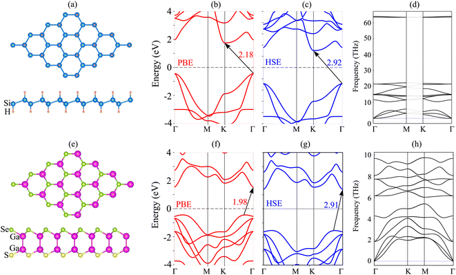 | ||
| Fig. 1 (a and e) The optimized atomic structure, (b and f) PBE band structure, (c and g) HSE band structure and (d and h) phonon spectra of (a–d) SiH and (e–h) Janus Ga2SSe monolayers. | ||
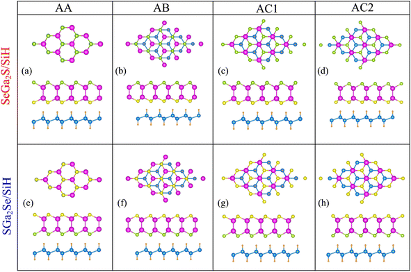
We now design the composed heterostructure, generated from Janus Ga2SSe and SiH monolayers. Owing to the small difference in the lattice parameters between Janus Ga2SSe and SiH monolayers, to design the Ga2SSe/SiH heterostructure, we use a (1 × 1) unit cell of the Ga2SSe monolayer to match with a (1 × 1) unit cell of the SiH monolayer. The lattice parameter of the composed Ga2SSe/SiH heterostructure is obtained to be 3.80 Å, giving rise to a small lattice mismatch of about 1.7%. This small lattice mismatch makes the heterostructure energetically favorable and suggests that it can be synthesized easily in experiments. The out-of-plane symmetry in the Janus Ga2SSe monolayer leads to the formation of two different types of Ga2SSe/SiH heterostructure, namely SGa2Se/SiH and SeGa2S/SiH stacking patterns. Additionally, each stacking pattern of the Ga2SSe/SiH heterostructure includes four different stacking configurations, including AA, AB, AC1 and AC2. All stacking configurations of the Ga2SSe/SiH heterostructure are depicted in Fig. 2. After geometric optimization, we can obtain the interlayer separation d between the hydrogen layer in the SiH layer and the sulfur (selenide) layer in the Janus Ga2SSe layer, which is listed in Table 1. One can find that the interlayer separation of the Ga2SSe/SiH heterostructure for different stacking configurations is in the range from 2.22 to 2.27 Å. The AC2 stacking configuration of the SGa2Se/SiH heterostructure is considered to be the most energetically stable because of the shortest interlayer separation and the lowest binding energy. Furthermore, one can find that the binding energy of the Ga2SSe/SiH heterostructure is consistent with that of previously reported SiH-based heterostructures.29 Furthermore, it can be seen from Table 1 that the binding energy of the SGa2Se/SiH heterostructure is lower than that of the SeGa2S/SiH heterostructure. The reason for such a difference is that the electronegativity of Se atoms is slightly higher than that of S atoms. This finding was also observed in previous reports.35–37
| Stacking configuration | d, Å | Eb, meV Å−2 | Eg, eV | Band alignment | |
|---|---|---|---|---|---|
| SeGa2S/SiH | AA | 2.25 | −10.93 | 0.68 | Type-II |
| AB | 2.24 | −11.19 | 0.70 | Type-II | |
| AC1 | 2.25 | −11.23 | 0.68 | Type-II | |
| AC2 | 2.27 | −10.95 | 0.66 | Type-II | |
| SGa2Se/SiH | AA | 2.26 | −11.65 | 0.93 | Type-II |
| AB | 2.23 | −11.86 | 0.97 | Type-II | |
| AC1 | 2.25 | −11.84 | 0.96 | Type-II | |
| AC2 | 2.22 | −11.95 | 0.92 | Type-II | |
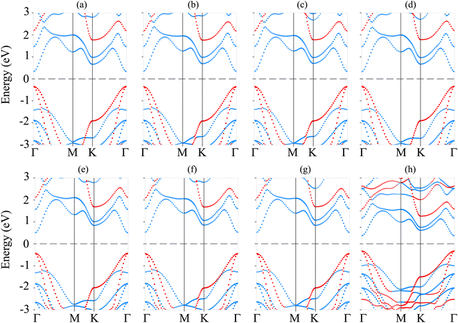
The electronic band structures of the Ga2SSe/SiH heterostructure for different stacking configurations are depicted in Fig. 3. One can find that all stacking configurations of the Ga2SSe/SiH heterostructure are semiconductors with direct band gaps. Both the CBM and VBM of the Ga2SSe/SiH heterostructure for all stacking configurations are located at the Γ point. Thus, the generation of the Ga2SSe/SiH heterostructure leads to conversion from indirect semiconductors in the constituent Ga2SSe and SiH monolayers to a direct semiconductor. Furthermore, the band gaps of the Ga2SSe/SiH heterostructure are listed in Table 1. It is obvious that the band gaps of the SeGa2S/SiH heterostructure are smaller than those of the SGa2Se/SiH heterostructure. The average band gap of the SeGa2S/SiH heterostructure is about 0.68 eV, while it is 0.95 eV for the SGa2Se/SiH heterostructure. However, these values of the band gaps of the composed Ga2SSe/SiH heterostructure for all stacking configurations are smaller than those of the constituent Ga2SSe and SiH monolayers. Thus, the generation of the Ga2SSe/SiH heterostructure gives rise to a reduction in the band gap, demonstrating that the electrons move faster from the valence bands to the conductions bands.
Interestingly, when the Ga2SSe/SiH heterostructure is formed, it leads to the formation of type-I, type-II or type-III band alignment. According to the contributions of the Ga2SSe and SiH layers to the band structures of the Ga2SSe/SiH heterostructure, we find that all stacking configurations of the Ga2SSe/SiH heterostructure form type-II band alignment. The CBM of the Ga2SSe/SiH heterostructure for all considered stacking configurations is contributed by the Ga2SSe layer, while the VBM is dominated by the SiH layer. The formation of type-II band alignment in the Ga2SSe/SiH heterostructure indicates that the photogenerated carriers are separated effectively, enhancing the photocatalytic performance.
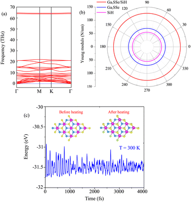
As discussed above, the AC2 stacking configuration of the SGa2Se/SiH heterostructure is the most energetically favorable stacking pattern; we thus focus on this pattern in all the following discussion. First, we check its dynamical, mechanical and thermodynamical stability by calculating the phonon spectrum and elastic constants, and performing ab initio molecular dynamics simulation, as depicted in Fig. 4. The phonon dispersion curves of the SGa2Se/SiH heterostructure shown in Fig. 4(a) show that all frequencies are positive, suggesting that such a heterostructure is dynamically stable in the ground state. The mechanical properties are examined to evaluate the mechanical stability of the heterostructure. The elastic constants can be obtained by calculating six different finite distortions of the lattice from the stress–strain relation as follows:38
 | (2) |
Our calculations show that there are two independent elastic constants, which are calculated to be C11 = 133.26 N m−1 and C12 = 30.21 N m−1. One can find that these values of the elastic constants of the Ga2SSe/SiH heterostructure meet the Born–Huang criteria, i.e. C11 > 0 and C11 − C12 > 0. This finding suggests that the Ga2SSe/SiH heterostructure is mechanically stable. Additionally, the Young’s modulus Y = (C112 − C122)/C11 of the Ga2SSe/SiH heterostructure is depicted in Fig. 4(b). The calculated Young’s moduli for the Ga2SSe/SiH heterostructure, and isolated Ga2SSe and SiH monolayers are obtained to be 126.41, 69.73 and 55.17 N m−1, respectively. One can find that the Young’s modulus of the Ga2SSe/SiH heterostructure is still greater than that of both the Ga2SSe and SiH monolayers, confirming satisfactory mechanical stability. The thermal stability of the Ga2SSe/SiH heterostructure is also evaluated by performing AIMD simulation, as shown in Fig. 4(c). It is obvious that there is a small fluctuation of the total energy and no observed structural deformation in the Ga2SSe/SiH heterostructure, confirming that it is thermally stable at room temperature.
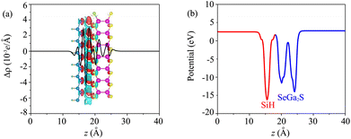
Moreover, when the Ga2SSe/SiH heterostructure is formed, it leads to redistribution of charges. The charge redistribution of the Ga2SSe/SiH heterostructure can be visualized as follows:
| Δρ = ρH − ρM1 − ρM2 | (3) |
Furthermore, for the use of the Ga2SSe/SiH heterostructure as a building block in high-performance electronic devices, it is important to check the transport properties, including effective mass and carrier mobility. The carrier mobility of 2D materials can be calculated as follows:
 | (4) |
 . md is the average of the effective masses along the x and y directions,
  . It should be noted that the effective mass can be obtained as follows:
 | (5) |
 | (6) |
 | (7) |
| Materials | Carriers | Cx2D | Cy2D | Exd | Eyd | μx | μy | ||
|---|---|---|---|---|---|---|---|---|---|
| SiH | Electrons | 72.54 | 68.99 | 3.728 | −9.636 | 1.72 | 0.126 | 139 | 20 |
| Holes | 72.54 | 68.99 | −3.248 | −3.224 | −0.62 | −0.569 | 397 | 383 | |
| Ga2SSe | Electrons | 90.13 | 90.13 | −10.792 | −10.792 | 0.267 | 0.291 | 221 | 203 |
| Holes | 90.13 | 90.13 | −2.226 | −2.226 | −1.34 | −2.77 | 150 | 73 | |
| SGa2Se/SiH | Electrons | 176.88 | 167.84 | −9.856 | −9.856 | 0.25 | 0.138 | 635 | 603 |
| Holes | 176.88 | 167.84 | −5.324 | −5.324 | 0.529 | 0.559 | 461 | 438 | |
| SeGa2S/SiH | Electrons | 171.8 | 171.9 | −9.885 | −9.91 | 0.269 | 0.291 | 497 | 457 |
| Holes | 171.8 | 171.9 | −5.28 | −5.285 | −0.586 | −0.535 | 400 | 437 |
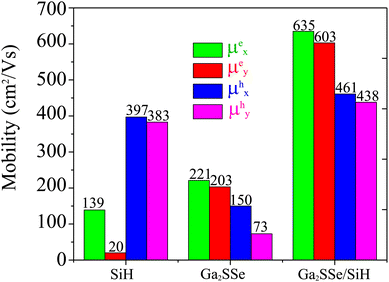 | ||
| Fig. 6 Carrier mobility for electrons and holes of SiH, Ga2SSe and the Ga2SSe/SiH heterostructure in the x and y directions. | ||
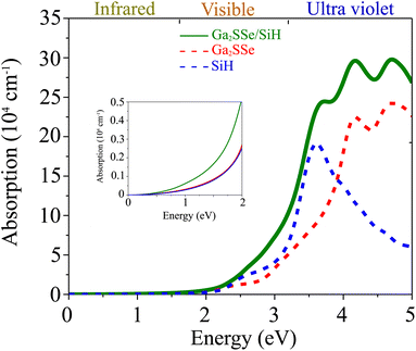
Furthermore, in view of the practical applications, it is necessary to investigate the optical properties of the heterostructure. Thus, we further calculate the optical absorption coefficient of the Ga2SSe/SiH heterostructure as follows:
 | (8) |
4 Conclusions
In conclusion, we have constructed the SiH/Ga2SSe heterostructure with different stacking patterns using first-principles prediction. The electronic, mechanical, transport and optical properties of the most energetically favorable stacking pattern are investigated to evaluate its potential in high-efficiency applications. The SiH/Ga2SSe heterostructure is thermodynamically, mechanically and energetically stable at room temperature. The band gaps of the SiH/Ga2SSe heterostructure are smaller than those of the constituent SiH and Ga2SSe monolayers, suggesting that the optical absorption of such a heterostructure can be improved. The SiH/Ga2SSe heterostructure is a semiconductor with a direct band gap of about 0.68 or 0.95 eV, depending on the stacking pattern. The SiH/Ga2SSe heterostructure forms type-II band alignment for all stacking patterns, indicating that the photogenerated carriers are separated effectively, thus enhancing the photocatalytic performance. Moreover, the carrier mobilities for electrons and holes of the Ga2SSe/SiH heterostructure are higher than those of the constituent SiH and Ga2SSe monolayers in both the x and y directions, suggesting that the performances of electronic devices based on the Ga2SSe/SiH heterostructure would be excellent and reliable. The formation of the Ga2SSe/SiH heterostructure also gives rise to an enhancement of the absorption coefficient in both the visible and ultraviolet regions. Our findings could give valuable guidance for the design of high-efficiency devices based on the SiH/Ga2SSe heterostructure.Conflicts of interest
There are no conflicts to declare.References
- K. S. Novoselov, A. K. Geim, S. V. Morozov, D.-e. Jiang, Y. Zhang, S. V. Dubonos, I. V. Grigorieva and A. A. Firsov, Science, 2004, 306, 666–669 CrossRef CAS PubMed.
- L. Song, L. Ci, H. Lu, P. B. Sorokin, C. Jin, J. Ni, A. G. Kvashnin, D. G. Kvashnin, J. Lou and B. I. Yakobson, et al., Nano Lett., 2010, 10, 3209–3215 CrossRef CAS PubMed.
- M. Batmunkh, M. Bat-Erdene and J. G. Shapter, Adv. Mater., 2016, 28, 8586–8617 CrossRef CAS PubMed.
- W. Choi, N. Choudhary, G. H. Han, J. Park, D. Akinwande and Y. H. Lee, Mater. Today, 2017, 20, 116–130 CrossRef CAS.
- A. S. Sarkar and E. Stratakis, Adv. Sci., 2020, 7, 2001655 CrossRef CAS PubMed.
- J. Pang, A. Bachmatiuk, Y. Yin, B. Trzebicka, L. Zhao, L. Fu, R. G. Mendes, T. Gemming, Z. Liu and M. H. Rummeli, Adv. Energy Mater., 2018, 8, 1702093 CrossRef.
- C. Klinkert, Á. Szabó, C. Stieger, D. Campi, N. Marzari and M. Luisier, ACS Nano, 2020, 14, 8605–8615 CrossRef CAS PubMed.
- B. Luo, G. Liu and L. Wang, Nanoscale, 2016, 8, 6904–6920 RSC.
- K. I. Bolotin, K. J. Sikes, Z. Jiang, M. Klima, G. Fudenberg, J. Hone, P. Kim and H. L. Stormer, Solid State Commun., 2008, 146, 351–355 CrossRef CAS.
- B. Zhan, C. Li, J. Yang, G. Jenkins, W. Huang and X. Dong, Small, 2014, 10, 4042–4065 CrossRef CAS PubMed.
- W. Zhu, T. Low, H. Wang, P. Ye and X. Duan, 2D Materials, 2019, 6, 032004 CrossRef CAS.
- X. Song, Z. Guo, Q. Zhang, P. Zhou, W. Bao and D. W. Zhang, Small, 2017, 13, 1700098 CrossRef.
- M. S. Jang, H. Kim, Y.-W. Son, H. A. Atwater and W. A. Goddard III, Proc. Natl. Acad. Sci. U. S. A., 2013, 110, 8786–8789 CrossRef CAS.
- L. Kou, C. Chen and S. C. Smith, J. Phys. Chem. Lett., 2015, 6, 2794–2805 CrossRef CAS PubMed.
- J. Pei, X. Gai, J. Yang, X. Wang, Z. Yu, D.-Y. Choi, B. Luther-Davies and Y. Lu, Nat. Commun., 2016, 7, 1–8 Search PubMed.
- A.-Y. Lu, H. Zhu, J. Xiao, C.-P. Chuu, Y. Han, M.-H. Chiu, C.-C. Cheng, C.-W. Yang, K.-H. Wei and Y. Yang, et al., Nat. Nanotechnol., 2017, 12, 744–749 CrossRef CAS.
- X. Wan, E. Chen, J. Yao, M. Gao, X. Miao, S. Wang, Y. Gu, S. Xiao, R. Zhan and K. Chen, et al., ACS Nano, 2021, 15, 20319–20331 CrossRef CAS PubMed.
- L. Zhang, Z. Yang, T. Gong, R. Pan, H. Wang, Z. Guo, H. Zhang and X. Fu, J. Mater. Chem. A, 2020, 8, 8813–8830 RSC.
- T. Hu, F. Jia, G. Zhao, J. Wu, A. Stroppa and W. Ren, Phys. Rev. B, 2018, 97, 235404 CrossRef CAS.
- Y. Luo, M. Sun, J. Yu and U. Schwingenschlogl, Chem. Mater., 2021, 33, 4128–4134 CrossRef CAS.
- Q. Wu, L. Cao, Y. S. Ang and L. K. Ang, Nano Express, 2020, 1, 010042 CrossRef.
- Y. Yu, J. Zhou, Z. Guo and Z. Sun, ACS Appl. Mater. Interfaces, 2021, 13, 28090–28097 CrossRef CAS PubMed.
- Y. Guo, S. Zhou, Y. Bai and J. Zhao, Appl. Phys. Lett., 2017, 110, 163102 CrossRef.
- B. Sa, X. Shen, S. Cai, Z. Cui, R. Xiong, C. Xu, C. Wen and B. Wu, Phys. Chem. Chem. Phys., 2022, 24, 15376–15388 RSC.
- M. Houssa, E. Scalise, K. Sankaran, G. Pourtois, V. Afanas’ Ev and A. Stesmans, Appl. Phys. Lett., 2011, 98, 223107 CrossRef.
- J. Qiu, H. Fu, Y. Xu, Q. Zhou, S. Meng, H. Li, L. Chen and K. Wu, ACS Nano, 2015, 9, 11192–11199 CrossRef CAS PubMed.
- J. Zeng, L. Xu, X. Luo, B. Peng, Z. Ma, L.-L. Wang, Y. Yang and C. Shuai, Phys. Chem. Chem. Phys., 2021, 23, 2812–2818 RSC.
- S. Han, Y. Li, J. Chai and Z. Wang, Phys. Chem. Chem. Phys., 2020, 22, 8565–8571 RSC.
- S. Han, Y. Li and Z. Wang, Phys. Chem. Chem. Phys., 2020, 22, 17145–17151 RSC.
- G. Kresse and J. Furthmüller, Phys. Rev. B: Condens. Matter Mater. Phys., 1996, 54, 11169 CrossRef CAS.
- J. P. Perdew, K. Burke and M. Ernzerhof, Phys. Rev. Lett., 1996, 77, 3865 CrossRef CAS PubMed.
- S. Grimme, J. Antony, S. Ehrlich and H. Krieg, J. Chem. Phys., 2010, 132, 154104 CrossRef PubMed.
- S. Grimme, S. Ehrlich and L. Goerigk, J. Comput. Chem., 2011, 32, 1456–1465 CrossRef CAS PubMed.
- J. Heyd, G. E. Scuseria and M. Ernzerhof, J. Chem. Phys., 2003, 118, 8207–8215 CrossRef CAS.
- Y.-L. Liu, W.-K. Zhao, Y. Shi and C.-L. Yang, Phys. Chem. Chem. Phys., 2021, 23, 9440–9447 RSC.
- C. Yu and Z. Wang, Phys. Status Solidi B, 2019, 256, 1900261 CrossRef CAS.
- X. B. Yuan, Y. H. Guo, J. L. Wang, G. C. Hu, J. F. Ren and X. W. Zhao, Front. Chem., 2022, 10, 861838 CrossRef CAS PubMed.
- W.-Z. Xiao, G. Xiao and L.-L. Wang, J. Chem. Phys., 2016, 145, 174702 CrossRef PubMed.
- Z. Cui, K. Ren, Y. Zhao, X. Wang, H. Shu, J. Yu, W. Tang and M. Sun, Appl. Surf. Sci., 2019, 492, 513–519 CrossRef CAS.
- M. Cao, L. Ni, Z. Wang, J. Liu, Y. Tian, Y. Zhang, X. Wei, T. Guo, J. Fan and L. Duan, Appl. Surf. Sci., 2021, 551, 149364 CrossRef CAS.
| This journal is © The Royal Society of Chemistry 2022 |

