
 Open Access Article
 This Open Access Article is licensed under a Creative Commons Attribution-Non Commercial 3.0 Unported Licence
Performance characterization of transparent and conductive grids one-step-printed on curved substrates using template-guided foaming†
Youngchul Chae,
Juyeol Bae ,
Kyoungyoung Lim and
Taesung Kim*
,
Kyoungyoung Lim and
Taesung Kim*
Department of Mechanical Engineering, Ulsan National Institute of Science and Technology (UNIST), 50 UNIST-gil, Ulsan, 44919, Republic of Korea. E-mail: tskim@unist.ac.kr; Fax: +82-52-217-2409; Tel: +82-52-217-2313
First published on 29th September 2022
Abstract
Next-generation electronic devices require electrically conductive, mechanically flexible, and optically transparent conducting electrodes (CEs) that can endure large deformations. However, patterning conditions of such CEs have been mainly limited to flat substrates because of the nature of conventional fabrication techniques; thus, comprehensive studies are needed to be conducted on this topic. Herein, we characterize the material and structural properties of CEs, curvature of substrates, and their operational performance. We use a single-step printing method, termed template-guided foaming (TGF), to fabricate flexible transparent conducting electrodes (FTCEs) on various substrates with initial curvatures. We adopted silver nanowires (AgNWs) and a conductive polymer (PEDOT:PSS) to characterize and compare the effect of initial substrate curvatures on the sheet resistance during inward and outward bending. The AgNW-based grids exhibited a considerably low sheet resistance, which was linearly proportional to the working curvature of the substrate, whereas PEDOT:PSS-based grids exhibited a relatively higher sheet resistance, which increased regardless of the initial and working curvatures of the substrate. Although both CE grids exhibited a high flexibility and transmittance during 10![[thin space (1/6-em)]](https://www.rsc.org/images/entities/char_2009.gif) 000 cyclic tests, the initial curvature of the substrate affected the sheet resistance; hence, operational conditions of FTCEs must be considered to improve the repeatability and durability of such FTCE-integrated devices. Finally, we believe that our study introduces a novel methodology for the design, fabrication, and operation strategy of flexible electronic devices and wearable devices with high performances.
000 cyclic tests, the initial curvature of the substrate affected the sheet resistance; hence, operational conditions of FTCEs must be considered to improve the repeatability and durability of such FTCE-integrated devices. Finally, we believe that our study introduces a novel methodology for the design, fabrication, and operation strategy of flexible electronic devices and wearable devices with high performances.
Introduction
Flexible transparent conducting electrodes (FTCEs) are key components in a wide range of electronic research fields and application markets, such as wearable devices,1 solar cells,2 organic light emitting diodes,3 touchscreens,4,5 and displays,6 owing to their unique electrical characteristics, flexibility, and portability. In previous studies, conductive nanomaterials, such as nanowires, were applied as electrodes using techniques such as capillary printing and NanoDrip printing.7,8 In general, indium tin oxide (ITO) has been widely used as a transparent electrode material in commercial products using the conventional method of patterning an electrode on flat substrates.9 However, the scarcity and high-cost of indium and the particularly high brittleness of the ITO electrodes, which crack easily even when exposed to a moderate mechanical stress, limit their application in flexible devices.10 In addition, as the demand for wearable devices that are lightweight, portable, and durable is increasing, significant efforts have been devoted to patterning transparent electrodes on curved substrates.11 Therefore, FTCEs,12 carbon nanotubes,13 metal nanowires,14 graphene,15 silver nanowires (AgNWs),16 copper NWs,17,18 and other conductive nanomaterials have been used as alternatives to ITO.19–21 Furthermore, after patterning on substrates such as glass, quartz, and polyethylene terephthalate (PET), preliminary studies have been conducted to investigate electrical and mechanical properties using bending and tensile tests.22–24 However, because of the limitations of standard photo-lithography processes based on two-dimensional (2D) flat substrates, the one-step patterning on three-dimensional (3D) curved substrates remains a challenge. Moreover, the high cost of the nanofabrication equipment and considerable time-consumption of the serial writing process are critical issues in the wearable electronics industry.25One-step printing on 3D substrates with initial curvatures, which is an intriguing research field, can address the weaknesses of the existing patterning and printing technologies, as it facilitates the patterning of electrodes on arbitrary 3D substrates. We developed the template-guided foaming (TGF) method, which is a promising one-step printing method, using a flexible template with a through-hole and post arrays. The developed method is based on a liquid-mediated patterning approach that allows the mixed scale micro/nano 3D conformal printing of various nanomaterials via facile and simple steps.26,27 In addition, the template mold has a monolithic design; it is not only flexible but also mechanically strong owing to the material properties of off-stoichiometry thiol–ene polymer resin (OSTEMER), with a Young's modulus of 1000 MPa.28 Furthermore, owing to the chemical resistance of OSTEMER, no restrictions are imposed on the use of aqueous nanomaterials, such as perovskite, photoresist, and organic semiconductors.29 Furthermore, the widespread use of flexible and/or wearable electronic devices is increasing. To the best of our knowledge, the performance characterization of FTCEs for such devices has not been investigated. In our previous study, the TGF method was employed to directly pattern silver nanoparticle grids on 3D substrates with various Gaussian curvatures, and changes in the sheet resistance were measured under deformed conditions.30 Although an one-step printing of conductive and transparent materials on 3D curved substrates is possible, the characterization of variations (repeatability) of the sheet resistance of such a CE-grid network considering the operational curvature of substrates and degree of fatigue (durability) of the patterned grids needs to be thoroughly studied. The performance of FTCEs might be significantly improved by applying the TGF method to wearable devices using a more effective approach. In addition, the sheet resistance changes must be investigated to verify whether it can be constant or recoverable after numerous repeated bendings.31
Herein, we adopted the TGF method to fabricate conductive grids on 2D flat and 3D curved substrates and investigated the functions and performances of FTCEs in terms of the electrical conductivity, flexibility, repeatability, durability, and transparency. We produced silver-mesh FTCEs (SMFTCEs) and polymer-based FTCEs (PFTCEs) on various substrates using AgNWs and conductive polymers (poly(3,4-ethylenedioxythiophene):poly(styrenesulfonate) (PEDOT:PSS)) and subsequently analyzed their electrical, mechanical, and optical properties as the substrates underwent a large degree of bending deformation. Additionally, we investigated the effect of the initial curvature of substrates on the sheet resistance over time. Consequently, we believe that this study can provide guidelines on one-step printing methods for fabricating FTCEs for wearable electronic devices, foldable surface devices, displays, etc.
Materials and methods
Reagents and materials
Polydimethylsiloxane (PDMS; Sylgard 184, Dow Corning), OSTEMER (OSTEMER 322 Crystal Clear, Mercene Labs), and poly(vinyl alcohol) (PVA; Mw 89000–98000, 99+% hydrolyzed, 341584, Sigma Aldrich) were used to fabricate through-holes and post arrays. Chlorotrimethylsilane (TMSCI; 386529, Sigma-Aldrich), and trichloro(1H,1H,2H,2H-perfluorooctyl)silane (PFOCTS; 448931, Sigma-Aldrich) were used for the surface modification of the through-holes and post arrays. AgNW dispersions (20 nm × 20 μm, Novarials) and PEDOT:PSS (Sigma Aldrich) were used as provided by the manufacturer. Polycarbonate (PC), PET, and glass were used as substrates.
Fabrication of molds with through-holes and post arrays
A previously reported method was employed to fabricate a mold with a through-hole and post arrays.32 An SU-8 master mold was utilized to fabricate microfluidic devices, and a standard photolithography process was used, as shown in Fig. S1.† A negative photoresist (SU-8 2050, Kayaku Advanced Materials) was spin-coated onto a silicon wafer to a height of 50 μm and subsequently soft-baked. After exposure to the ultraviolet (UV) light using a photomask and mask aligner (MA6, SussMicroTec), a post-exposure bake process was performed. Before applying the photoresist to the second layer, hexamethyldisilazane (HMDS, 440191, Sigma-Aldrich) was spin-coated to increase the adhesion between the wafer and photoresist; subsequently, it was soft-baked. The second layer was spin-coated to a height of 25 μm using the photoresist (SU-8 2025, Kayaku Advanced Materials) and soft-baked. After the UV-light exposure using a second photomask and mask aligner, post-exposure baking was performed, followed by immersion in a SU-8 developer (Kayaku Advanced Materials) to remove the unexposed photoresist. The photolithography process was completed after hard-baking this wafer. To obtain a PDMS mold, PFOCTS was used to chemically functionalize the SU-8 master mold surface into a hydrophobic surface. During the soft lithography process, a 10:1 mixture of the PDMS base and curing agent was degassed in vacuum for 30 min. The PDMS mixture was poured into the SU-8 master mold and then cured in an oven for 3 h at 65 °C. The replicated PDMS mold was detached from the SU-8 mater mold, and the surface was chemically functionalized using TMSCI.
To fabricate an OSTEMER membrane with through-holes and post arrays, a water-soluble sacrificial layer was created by spin-coating PVA on the glass, and the PDMS mold was placed on it. Subsequently, to generate a negative pressure in the microchannel between the PDMS mold and water-soluble sacrificial PVA layer on the glass, the air in the PDMS mold was degassed by placing it in a vacuum state, and an OSTEMER resin was injected through the inlet hole. The PDMS mold and water-soluble sacrificial PVA layer on the glass remained in contact via the van der Waals interaction, while the OSTEMER resin was loaded. After loading, the OSTEMER resin was solidified by placing it in the UV light with a wavelength of 365 nm for 5 min. The PDMS mold was detached; it was reusable. The solidification of the OSTEMER resin was completed by placing it in an oven for 3 h at 90 °C. The sacrificial PVA layer was dissolved in deionized water to detach the through-hole and post array membrane from the glass.
Experimental setup
An inverted fluorescence microscope (IX71, Olympus Corp.), equipped with a charge-coupled device camera (Clara Interline CCD, Andor Technology Ltd.), was used to observe and analyze the liquid patterning process. The microscope was automated using a motorized stage (BioPrecision2), motorized focus controller (99A400), and controller system (MAC 6000) manufactured by Ludl Electronic Products. To control atmospheric conditions, a customized humidity/temperature controlling system, comprising solenoid valves (S10MM-20-24-2, Pneumadyne Inc.), a humidity/temperature sensor (SHT15, Sensirion), and a microcontroller board (Arduino Uno R3, Arduino cc.), was programmed using the LabVIEW software (National Instruments Corp.). During the experiments with this microscope, images were captured using an imaging software (MetaMorph v7.8.10.0, Molecular Devices). The fluorescence intensities of the images were quantitatively analyzed using the ImageJ software (National Institutes of Health, Bethesda). The normalized fluorescence intensities were plotted using the OriginPro 2020 software (OriginLab Corp.). High-resolution scanning electron microscopy (SEM) images were captured using a field emission (FE) scanning electron microscope (S-4800, Hitachi) by sputtering a 2 nm platinum layer on the surface of the through-hole and post arrays. An ultraviolet-visible-near-infrared (UV-Vis-NIR) spectrophotometer (Cary 5000, Agilent) was used to measure the transmittance of SMFTCEs and PFTCEs.Results and discussion
Operational principle of the one-step printing of AgNW-based conductive grids
We utilized the TGF method, developed in our previous study, to conduct the one-step printing of liquid-mediated nanomaterials on flat and curved substrates26,30 and generate conductive grid patterns on various substrates. As shown in Fig. 1a, the interlayer membrane is essential in the TGF method; hence, we redesigned and fabricated the membrane. The height of the membrane was 50 μm with a gap of 25 μm between its bottom surface and the target substrate. The diameter of the evaporation through-holes was 60 μm. The diameter of the posts was fixed at 30 μm, whereas the spacing between the post walls was changed from 40 to 50 μm because these geometrical dimensions are critical in forming TGF-based conductive grid patterns. Herein, we characterized and optimized them to achieve a high performance.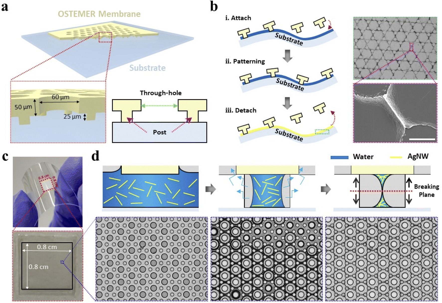 | ||
| Fig. 1 Schematic of the TGF process for the one-step printing of AgNWs onto various substrates. (a) Structure of an OSTEMER membrane with through-hole and post arrays. (b) One-step-printing process for conductive grids on a substrate. SEM images illustrate TGF-based AgNW grids on a PC substrate. Scale bar is 20 μm. (c) Optical images of a PC device on which AgNW grids are printed. (d) (Top) Illustration of the AgNW grid generation process (i.e., the patterning step in b.ii). These schematics depict the cross-sectional side view of the dotted square in (c) over time: suspension injection (left), evaporation of solution (middle), and foam-assisted pattern formation on the top membrane and bottom substrate (right). (Bottom) Optical images corresponding to the top illustrations obtained immediately after the printing steps. | ||
The TGF-based patterning process using the nanomaterial suspension solution is illustrated in Fig. 1b. AgNW-based conductive grids can be directly printed onto a substrate in three steps. In the first step, a AgNW suspension drop is pipetted onto the substrate, and then, the OSTEMER membrane was laid on it. This enables the spontaneous spreading of the drop into the membrane and fills all empty spaces, including the through-holes. The diameter and length of the AgNWs used were 20 nm and 20 μm, respectively. Surfactants were added to the AgNW suspension solution (e.g., 20 mg mL−1) to balance the Laplace and disjoining pressures; thus, the liquid films could be maintained at nanoscales without rupturing. We can imagine that AgNWs align with the liquid film as an evaporation-driven capillary flow is generated in the shearing/stretching direction between two neighboring posts. In the second step, AgNWs begin to move with the solution; in addition, their patterns are controlled by the pre-determined through-holes and post arrays during the evaporation in a single step. The complete evaporation of the AgNW suspension solution through the through-holes required approximately 3 min; thus, the AgNW grids were arranged by the capillary flow between the posts and then completely formed owing to the evaporation. In the third step, the OSTEMER membrane is detached from the substrate, which bisects the AgNW grid patterns horizontally, leaving one half on the top side of the substrate while maintaining the other half on the bottom side of the membrane along the breaking line/plane, as presented in Fig. 1d. Therefore, AgNWs are assembled in a nanoscale liquid foam structure, forming AgNW grid patterns.
We used silver nanoparticles (AgNPs) in our previous study to generate AgNP-based conductive grids on a curved surface.30 However, to maintain the electrical conductive properties, the substrate was not allowed to bend. Moreover, the AgNW-based conductive grids could overcome such a limitation because they were assembled in a mesh structure with numerous electric contacts between neighboring NWs. Therefore, SMFTCEs were facially patterned on a square with dimensions of 0.8 cm × 0.8 cm at the center of a flexible and transparent PC device, as shown in Fig. 1c. Although the PC device was bent repeatedly, its internal AgNW structures were not damaged, maintaining its electrical conductivity over time. The AgNW grid generation process is illustrated in Fig. 1d. Similar to our previous study, the basic unit of the membrane comprising a through-hole and post array can easily be scaled up to cover a large area because the evaporation flux per unit area is considerably uniform regardless of the scaled-up area. Thus, a large-area pattering can be completed within 3 min.
Characterization of AgNW-based conductive grids
We employed various substrates with different wettabilities and characterized the TGF-based patterning process of AgNW grids, as shown in Fig. 2. The patterning results of the AgNW grids depend on both the substrates and their wettability, as shown in Fig. 2a. We used a 20 mg mL−1 AgNW suspension with PC, PET, and glass substrates, which are typical transparent substrates used in conjunction with CEs. We used two types of PETs and glasses with two different contact angles (CAs), as shown at the top row in Fig. 2a. The PC substrates were hydrophobic, where CA was 99.9°; hence, AgNWs were completely constrained within the receding liquid flow, that is, Marangoni flow, during the evaporation process and continued to reside in the liquid film until the evaporation was completed.33 Therefore, the final concentration of AgNWs was relatively higher than that under other experimental conditions. Consequently, AgNW grids were clear, uniform, and densely agglomerated. Similarly, the experiment with a PET substrate (CA = 82.5°) produced comparable results. However, the glass and PET substrates were approximately super-hydrophilic; hence, AgNWs were spread widely and distributed randomly on the substrates. This phenomenon is more prominent with the glass substrates, which is attributed to nonspecific bindings; the glass substrates exhibited higher surface energy than that of the polymer-based substrates, interfering with the relocation of AgNWs with an evaporation-driven receding flow. Under this condition, it is assumed that AgNWs are relatively less agglomerated, which results in their sparse assembly. Consequently, hydrophobic substrates are preferable to generate uniform and dense AgNW grids on them.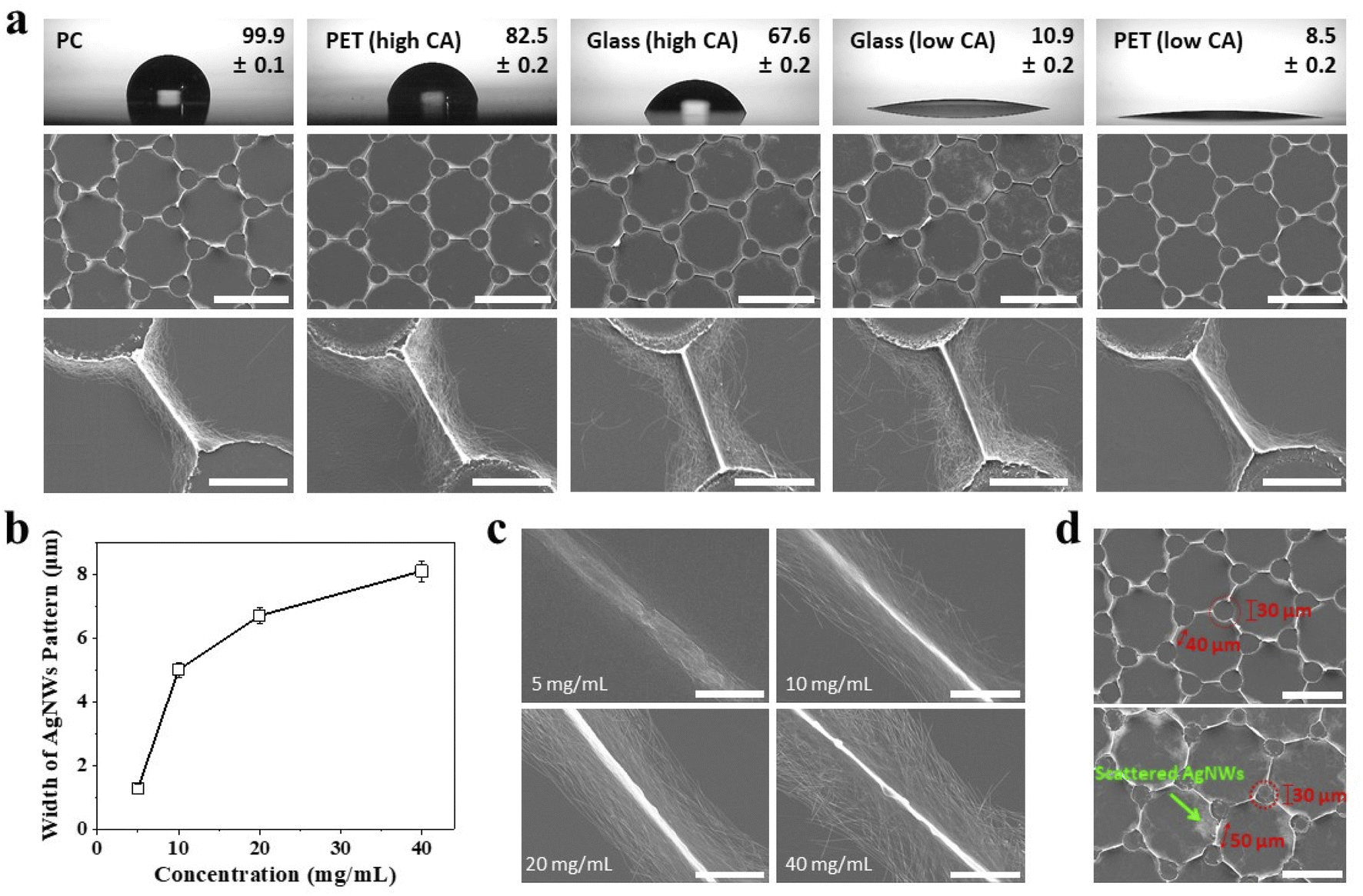 | ||
| Fig. 2 Formation of AgNW grids on various substrates. (a) AgNW grid formation on various flat substrates with different wettabilities. Droplet images depict the CAs of the substrates, and SEM images illustrate AgNW grid patterns. Scale bars are 100 (middle) and 20 μm (bottom). (b and c) Widths of the AgNW grids are affected by the concentration of the AgNW suspension (N = 15; measurements are obtained from five different locations of three different grids to achieve the average and standard deviation). Scale bars are 5 μm. (d) Effect of the spacing distance (wall to wall) between posts on the AgNW grids. AgNW grids are improved when the post diameter is 30 μm and the spacing distance between posts is 40 μm (top) compared to other conditions (bottom, post diameter = 30 μm and post spacing = 50 μm). Scale bars are 100 μm. | ||
In addition to the substrate wettability, the concentration of AgNW suspension solution may affect the final structure and density of AgNWs. As shown in Fig. 2b and c, we characterized the widths of AgNW grids patterned on PC by obtaining SEM images from five different locations in three different grids to calculate the average and standard deviation (N = 15). As expected, the width was proportional to the concentration because the more AgNWs were aggregated the higher the concentration wasm; thus, the width of the grids ranged from 1 to 8 μm as the concentration varied from 5 to 40 mg mL−1. We attempted to further reduce the width of the AgNW grids by decreasing the concentration to 5 mg mL; however, many defects developed in the AgNW grids, which resulted in a high sheet resistance. Furthermore, we investigated the effect of the post diameter and spacing between post walls on the performance of the AgNW grids. As shown in Fig. 2d, the optimal post diameter and spacing were 30 and 40 μm, respectively; therefore, the mesh-like densely aggregated AgNW grids were produced at widths in the sub-micron range with a concentration of 5 mg mL−1.
Additionally, we investigated the electrical properties of the AgNW grids patterned on the substrates. Fig. 3a illustrates the sheet resistance of the AgNW grids patterned on PC substrates with respect to the concentration of the AgNW suspension solution. After the AgNW grids were patterned, they were additionally annealed at 160 °C for 2 h to improve their electrical conductivity by removing any insulating surfactant residues around them. The higher the AgNW concentration, the lower the sheet resistance. This can be explained by the density and cohesion of the mesh-structured AgNWs after patterning and annealing and is attributed to the significantly high sheet resistance of AgNW grids formed with a low concentration of 10 mg mL−1. We examined the electrical properties of the AgNW grids one-step-printed on the curved PC substrates with four different initial curvatures (i.e., ρ0 = 0, 0.06, 0.1, and 0.14 mm−1), as shown in Fig. 3b. A AgNW suspension of 20 mg mL−1 was used, and an identical template was employed to eliminate any systematic errors. Sheet resistances varied in the range of 27.47–29.95 Ω sq−1, exhibiting a device-to-device variation of 8.6%. Notably, this error is even less than those caused by individual devices, implying that electrical conductivity is not affected by the initial curvature of substrates.
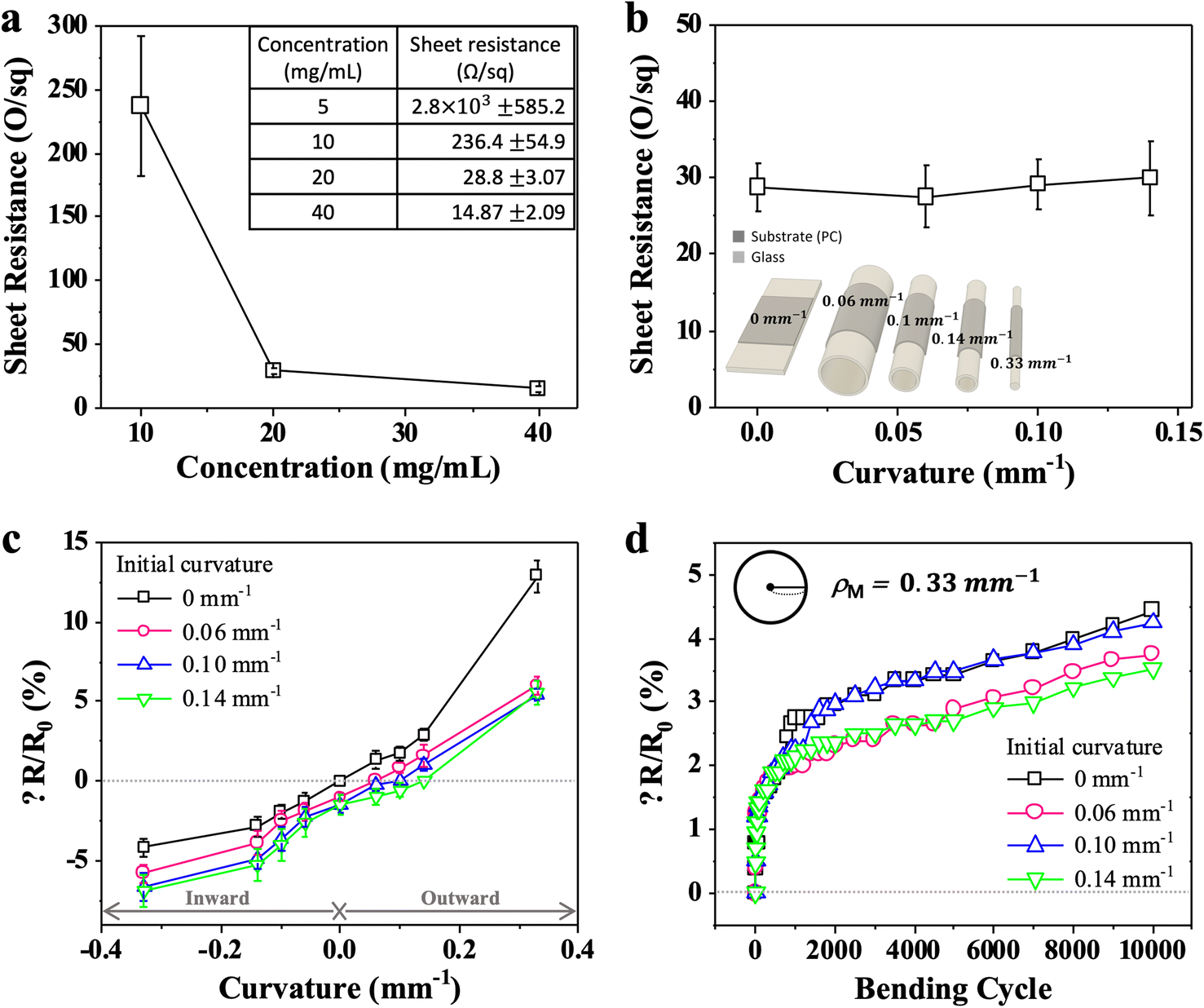 | ||
| Fig. 3 Characterization of the sheet resistance of AgNW grids produced using the TGF methods. (a) Sheet resistance change with respect to the concentration of AgNW suspensions. (b) Sheet resistances of the AgNW grids one-step-printed on the substrates with various initial curvatures, as shown in the insets (i.e., ρ0 = 0, 0.06, 0.10, and 0.14 mm−1). After one-step printing, no additional bending was applied to the substrates. (c) Sheet resistance changes in the AgNW grids when the substrates were additionally bent outward (positive curvatures) and inward (negative curvatures). Grey dotted line represents the initial curvature state in which no additional bending was applied to the grids/substrates. (d) Repeatability and durability test results of the AgNW grids that were patterned on the substrates with initial bending curvatures and then bent to the maximal curvature of ρM = 0.33 mm−1. | ||
We continued to measure the sheet resistance of the AgNW grids patterned on the PC substrates by bending the substrates at different pre-defined curvatures, as shown in Fig. 3c. First, we confirmed that changes in the sheet resistance were negligible regardless of the bending axis, that is, horizontal or vertical. This is because the AgNW grids are hexagonal; hence, they undergo an isotropic bending in 2D plane structures (e.g., thin PC film). When the AgNW grids patterned on a flat substrate were repeatedly bent inward and outward to the maximal curvature of ρM = 0.33 mm−1, the sheet resistance increased, and the sheet resistance change was approximately 12%. Moreover, when the AgNW grids patterned on the substrates with initial curvatures of ρ0 = 0, 0.06, 0.10, and 0.14 mm−1 were bent to ρM = 0.33 mm−1, the sheet resistance change was approximately 6%. Significantly, the sheet resistance increased almost linearly as the curvatures of the AgNW grids were shifted from negative (inward bending) to positive (outward bending), regardless of initial curvatures of the substrates; here, ΔR = R − R0, where R and R0 are the electrical resistance after and before bending, respectively. For a positive curvature, the mesh structures of AgNWs are wide open, decreasing the electrical conductivity. Conversely, the mesh structures for a negative curvature are closer to each other, which increases the number of mechanical contact junctions and decreases the electrical resistance. Therefore, a high and uniform electrical conductivity can be maintained when SMFTCEs are directly printed on a substrate with an initial curvature although both the initial and maximal bending curvatures need to be pre-determined at the device design stage.
As shown in Fig. 3d, we investigated the repeatability and durability of the AgNW grids by measuring the sheet resistance changes as the substrate was repeatedly bent inward and outward up to 10000 cycles. The maximal bending curvature was fixed at ρM = 0.33 mm−1. As the bending test began, the initial sheet resistance change (ΔR) significantly increased during the first ∼1000 cycles, followed by mild and linear increases for cycles in the range of 1000–10,000, regardless of initial curvatures of the AgNW grids. This can be attributed to the mechanical wear of AgNWs, which typically occurs at the early bending tests and slightly mitigates over time.
Evidently, both the repeatability and durability of all AgNW grids were high because of negligible changes in the sheet resistance, amounting to 3% to 4%. Notably, the closer the initial curvature of the substrate to the target curvature (i.e., ρM), the lower and more stable the sheet resistance change over time. Therefore, the AgNW grids need to be carefully designed and fabricated considering the target and printing curvatures of the substrate with respect to the performance of SMFTCEs.
Characterization of polymer-based conductive grids
PFTCEs were formed using the TGF method, as shown in Fig. 4. First, we employed PEDOT:PSS to fabricate FTCEs by directly printing the polymer on curved substrates similar to SMFTCEs and characterized their structural and electrical properties. As shown in Fig. 4a, the PEDOT:PSS grids were patterned on the PC substrates by changing their concentrations. At low concentrations (1 and 5 mg mL−1), thin and narrow grids were uniformly printed; however, their connections appeared to be locally and frequently broken. At high concentrations (10 and 20 mg mL−1), relatively thick and wide grids were printed; however, they were delaminated from the substrates; therefore, a concentration of 5 mg mL−1 was optimal. Subsequently, the sheet resistance of the flat PEDOT:PSS grids was measured to be 1944 Ω at the optimal concentration, as illustrated in Fig. 4b. As the concentration increased from 5 to 20 mg mL−1, the sheet resistance did not decrease. This can be attributed to the broken and delaminated grid patterns that are affected by the concentration. Additionally, we tested the PEDOT:PSS grids directly printed on the curved PC substrates with initial curvatures of ρ0 = 0, 0.06, 0.10, and 0.14 mm−1, as shown in Fig. 4c. Their sheet resistances were approximately identical regardless of the initial curvature. Although no additional bending was applied to the substrates, randomly broken and delaminated patterns, generated during the fabrication, caused relatively large errors.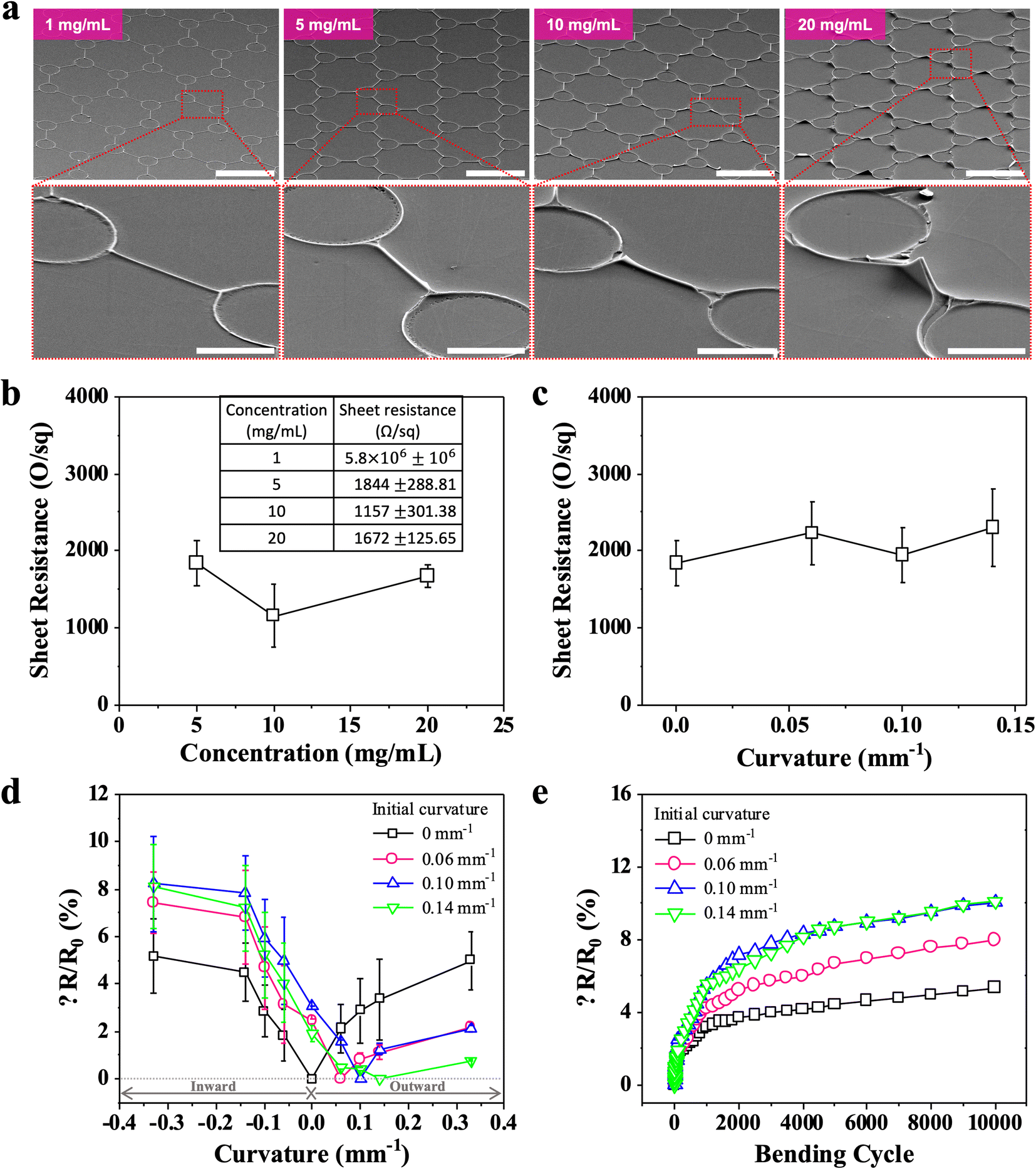 | ||
| Fig. 4 Characterization of the sheet resistance of the PEDOT:PSS-based conductive grids produced using the TGF method. (a) SEM images depict four different conductive PEDOT:PSS grids patterned using four different concentrations on the PC substrates. Scale bars are 100 (top) and 20 μm (bottom). (b) Sheet resistances of the PEDOT:PSS grids formed with four different concentrations. (c) Sheet resistances of the PEDOT:PSS grids patterned on the curved substrates, wherein initial curvatures remained during measurement (i.e., ρ0 = 0, 0.06, 0.10, and 0.14 mm−1). The concentration was fixed at 5 mg mL−1. (d) Sheet resistance changes of the PEDOT:PSS grids when the substrates were additionally bent outward (positive curvatures) and inward (negative curvatures). Gray dotted line represents the initial curvature state in which no additional bending was applied to the grids/substrates. (e) Repeatability and durability test results of the PEDOT:PSS grids that were patterned on the substrates with the initial bending curvatures and then bent to the maximal curvature of ρM = 0.33 mm−1. | ||
Similarly, we measured the sheet resistance of four PEDOT:PSS grids directly printed on the curved PC substrates with the same initial curvatures as previous measurements. As shown in Fig. 4d, when the PEDOT:PSS grids patterned on a flat substrate were repeatedly bent inward and outward to the maximal curvature of ρM = 0.33 mm−1, the sheet resistance change increased to approximately 5%. Unlike the linearly increasing sheer resistance changes exhibited by the mesh-structured AgNW grids, the measured sheet resistance changes were symmetrical with respect to the y-axis when they were bent inward and outward. This can be explained by the material and structural properties of the PEDOT:PSS grids: they may lose their conductivity during both outward (tensile stress) and inward (compressive stress) bending regardless of the initial curvature of substrates. However, the initial curvature of substrates affected the sheet resistance changes. First, the sheet resistance changes were asymmetrical with respect to the y-axis, and values increased as the substrates were bent inward, causing additional compression to the PEDOT:PSS grids. Therefore, the PEDOT:PSS grids undergo more sheet resistance changes under compression compared to those subjected to tension. Furthermore, we tested their repeatability and durability, as shown in Fig. 4e. The PEDOT:PSS grids, fabricated on a flat substrate, exhibited the smallest variation (<5% after 10000 cyclic tests). Moreover, the higher the initial curvatures, the larger the sheet resistance change (∼10%).
Characterization of the transmittance of SMFTCEs and PFTCEs
We tested the transmittance of the SMFTCE- and PFTCE-based devices, fabricated using the PC substrates, to demonstrate their performance as optoelectronic devices. Both the SMFTCE- and PFTCE-based devices are shown in Fig. 5a. For the former, 5 μL of the AgNW suspension solution was used at a concentration of 20 mg mL−1, whereas a PEDOT:PSS dispersion was used at the same volume and concentration for the latter. We measured the transmittance of the devices in the visible range of 400–800 nm, as shown in Fig. 5b and c. For the SMFTCE-based device, a transmittance in the range of 80–92% was obtained; the value was inversely proportional to the concentrations at a wavelength of 550 nm. For the PFTCE-based device, a transmittance in the range of 77–94% was measured at a wavelength of 550; the value followed the same concentration-dependent behavior. Consequently, both the SMFTCE- and PFTCE-based devices achieved an appropriate transparency while maintaining sub-micron CE grid networks for electronic applications.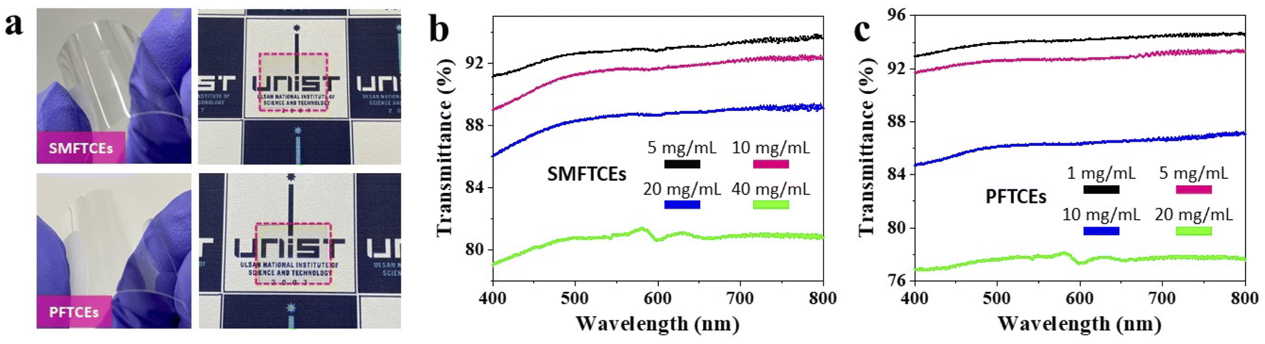 | ||
| Fig. 5 Characterization of transmittance of SMFTCEs and PFTCEs. (a) Photograph of an SMFTCE-patterned PC device (20 mg mL−1 AgNWs, top) and a PFTCE-patterned device (5 mg mL−1 PEDOT:PSS, bottom). (b) Optical transmittance of the SMFTCE-patterned PC devices fabricated with four different concentrations of 5, 10, 20, and 40 mg mL−1. (c) Optical transmittance of the PFTCE-patterned PC devices fabricated with four different concentrations of 1, 5, 10, and 20 mg mL−1 over the visible spectra. Bare PC substrate was used as a reference in the measurements. | ||
Conclusions
Herein, we demonstrated that the TGF platform could be employed to produce various conductive grids on flat and curved substrates. The platform utilizes a through-hole and post array-integrated thin membrane film to not only induce the evaporation of nanomaterial suspension solution but also generate CE grid patterns in a hybrid-scale and hierarchal manner with initially flat and curved substrates. In particular, the developed method enables the simultaneous generation of micro- and nano-scale patterns and can potentially increase the patterned area by maintaining a constant throughput. Because the TGF method can facilitate the large-scale and high-throughput patterning of AgNW suspension and polymer solution, we could produce AgNW- and PEDOT:PSS-based grids, respectively, on various curved substrates. This study revealed that initial curvatures of substrates affect the sheet resistance over time; AgNW-based grids exhibited extremely low sheet resistances, which increased as the working curvature of the substrate changed during inward to outward bending. Moreover, polymer-based grids exhibited a relatively high sheet resistance, which increased regardless of the initial and working curvature of the substrate. In general, both CE grids exhibited a high flexibility and transmittance; thus, operational conditions of FTCEs must be considered to improve the repeatability and durability of such FTCE-integrated devices. Finally, the target CE grids and their patterns can be manipulated in a facile and cost-effective manner by simply adopting appropriate nanomaterial suspension/solution. Consequently, this study introduced a promising strategy to design and fabricate next-generation flexible and transparent electronic devices, such as displays, touch screens, and wearable electronics.Author contributions
T. K. conceived this study. Y. C. and J. B. developed the microfluidic one-step-printing method. Y. C. performed all experiments with the aid of J. B. and K. L.; in addition, they analyzed the experimental data. All authors discussed the experimental results, wrote the manuscript, and approved it.Conflicts of interest
The authors declare no competing financial interest.Acknowledgements
This study was supported by National Research Foundation of Korea grants funded by the Korean government (NRF-2020R1A2C3003344 and NRF-2020R1A4A2002728).References
- Z. Zhong, K. Woo, I. Kim, H. Kim, P. Ko, D. Kang, S. Kwon, H. Kim, H. Youn and J. Moon, Small, 2018, 14, 1800676 CrossRef PubMed.
- M.-G. Kang, M.-S. Kim, J. Kim and L. J. Guo, Adv. Mater., 2008, 20, 4408–4413 CrossRef CAS.
- J.-G. Kim, J.-E. Lee, S. M. Jo, B. D. Chin, J.-Y. Baek, K.-J. Ahn, S. J. Kang and H.-K. Kim, Sci. Rep., 2018, 8, 1–13 Search PubMed.
- H. C. Chu, Y. C. Chang, Y. Lin, S. H. Chang, W. C. Chang, G. A. Li and H. Y. Tuan, ACS Appl. Mater. Interfaces, 2016, 8, 13009–13017 CrossRef CAS PubMed.
- Q. Zhou, J. G. Park, K. N. Kim, A. K. Thokchom, J. Bae, J. M. Baik and T. Kim, Nano Energy, 2018, 48, 471–480 CrossRef CAS.
- L. Li, B. Zhang, B. Zou, R. Xie, T. Zhang, S. Li, B. Zheng, J. Wu, J. Weng and W. Zhang, ACS Appl. Mater. Interfaces, 2017, 9, 39110–39115 CrossRef CAS.
- S. Kang, T. Kim, S. Cho, Y. Lee, A. Choe, B. Walker, S. J. Ko, J. Y. Kim and H. Ko, Nano Lett., 2015, 15, 7933–7942 CrossRef CAS PubMed.
- J. Schneider, P. Rohner, D. Thureja, M. Schmid, P. Galliker and D. Poulikakos, Adv. Funct. Mater., 2016, 26, 833–840 CrossRef CAS.
- H. B. Lee, W.-Y. Jin, M. M. Ovhal, N. Kumar and J.-W. Kang, J. Mater. Chem. C, 2019, 7, 1087–1110 RSC.
- D. J. Joe, S. Kim, J. H. Park, D. Y. Park, H. E. Lee, T. H. Im, I. Choi, R. S. Ruoff and K. J. Lee, Adv. Mater., 2017, 29, 1606586 CrossRef.
- X. Yu, D. Qi, Q. Zhang, D. Paeng, X. Han, A. Wang, D. Huang, L. Wang, Z. Zhang and S. Chen, Opt. Lett., 2020, 45, 901–904 CrossRef CAS PubMed.
- K. Rao, R. Gupta and G. U. Kulkarni, Adv. Mater. Interfaces, 2014, 1, 1400090 CrossRef.
- L. Hu, D. Hecht and G. Grüner, Nano Lett., 2004, 4, 2513–2517 CrossRef CAS.
- J.-Y. Lee, S. T. Connor, Y. Cui and P. Peumans, Nano Lett., 2008, 8, 689–692 CrossRef CAS PubMed.
- K. S. Kim, Y. Zhao, H. Jang, S. Y. Lee, J. M. Kim, K. S. Kim, J. H. Ahn, P. Kim, J. Y. Choi and B. H. Hong, Nature, 2009, 457, 706–710 CrossRef CAS PubMed.
- L. Hu, H. S. Kim, J.-Y. Lee, P. Peumans and Y. Cui, ACS Nano, 2010, 4, 2955–2963 CrossRef CAS PubMed.
- A. R. Rathmell, S. M. Bergin, Y. L. Hua, Z. Y. Li and B. J. Wiley, Adv. Mater., 2010, 22, 3558–3563 CrossRef CAS.
- Z. Zhong, H. Lee, D. Kang, S. Kwon, Y. M. Choi, I. Kim, K. Y. Kim, Y. Lee, K. Woo and J. Moon, ACS Nano, 2016, 10, 7847–7854 CrossRef CAS PubMed.
- A. Khan, Y. T. Huang, T. Miyasaka, M. Ikegami, S. P. Feng and W. D. Li, ACS Appl. Mater. Interfaces, 2017, 9, 8083–8091 CrossRef CAS PubMed.
- D. S. Hecht, L. Hu and G. Irvin, Adv. Mater., 2011, 23, 1482–1513 CrossRef CAS PubMed.
- P. E. Lyons, S. De, J. Elias, M. Schamel, L. Philippe, A. T. Bellew, J. J. Boland and J. N. Coleman, J. Phys. Chem. Lett., 2011, 2, 3058–3062 CrossRef CAS.
- Z. Wang, X. Yang, Z. Yang, W. Guo, L. Lin, N. Li, E. Jiang, J. Zhang, B. Yan and J. Ye, Front. Mater., 2019, 6, 18 CrossRef.
- Z. Zhong, S.-H. Lee, P. Ko, S. Kwon, H. Youn, J. Y. Seok and K. Woo, Nanoscale, 2020, 12, 2366–2373 RSC.
- J. Huang, Y. Lu, W. Wu, J. Li, X. Zhang, C. Zhu, Y. Yang, F. Xu and W. Song, J. Appl. Phys., 2017, 122, 195302 CrossRef.
- Z. Zhong, K. Woo, I. Kim, H. Hwang, S. Kwon, Y.-M. Choi, Y. Lee, T.-M. Lee, K. Kim and J. Moon, Nanoscale, 2016, 8, 8995–9003 RSC.
- J. Bae, J. Lee, Q. Zhou and T. Kim, Adv. Mater., 2019, 31, 1804953 CrossRef PubMed.
- J. Bae, K. Lee, S. Seo, J. G. Park, Q. Zhou and T. Kim, Nat. Commun., 2019, 10, 1–9 CrossRef PubMed.
- D. Sticker, M. Rothbauer, S. Lechner, M. T. Hehenberger and P. Ertl, Lab Chip, 2015, 15, 4542–4554 RSC.
- R. Geczy, D. Sticker, N. Bovet, U. O. Häfeli and J. P. Kutter, Lab Chip, 2019, 19, 798–806 RSC.
- J. Bae, Y. Chae, J. G. Park, R. Wu, J. Ju and T. Kim, ACS Appl. Mater. Interfaces, 2021, 13, 19168–19175 CrossRef CAS.
- D. Paeng, J. H. Yoo, J. Yeo, D. Lee, E. Kim, S. H. Ko and C. P. Grigoropoulos, Adv. Mater., 2015, 27, 2762–2767 CrossRef CAS PubMed.
- D. Tahk, S.-M. Paik, J. Lim, S. Bang, S. Oh, H. Ryu and N. L. Jeon, Lab Chip, 2017, 17, 1817–1825 RSC.
- K. Lee and T. Kim, J. Micromech. Microeng., 2021, 31, 105007 CrossRef CAS.
Footnote |
| † Electronic supplementary information (ESI) available. See https://doi.org/10.1039/d2ra05551a |
| This journal is © The Royal Society of Chemistry 2022 |