
 Open Access Article
 This Open Access Article is licensed under a Creative Commons Attribution-Non Commercial 3.0 Unported Licence
Electronic structure of strain-tunable Janus WSSe–ZnO heterostructures from first-principles†
E. A. Peterson ab,
T. T. Debelac,
G. M. Gomorod,
J. B. Neatonaef and
G. A. Asres*g
ab,
T. T. Debelac,
G. M. Gomorod,
J. B. Neatonaef and
G. A. Asres*g
aDepartment of Physics, University of California Berkeley, Berkeley, CA 94720, USA
bLiquid Sunlight Alliance, Lawrence Berkeley National Laboratory, Berkeley, CA 94720, USA
cInstitute for Application of Advanced Materials, Jeonju University, Conju, Chonbuk 55069, Republic of Korea
dFaculty of Engineering and Technology, Mechanical Engineering Department, Assosa University, Assosa, Ethiopia
eMaterials Science Division, Lawrence Berkeley National Laboratory, Berkeley, CA 94720, USA
fKavli Energy Nanosciences Institute, Berkeley, CA 94720, USA
gCenter for Materials Engineering, Addis Ababa Institute of Technology, Addis Ababa University, School of Multidisciplinary Engineering, Addis Ababa, 1000, Ethiopia. E-mail: georgies.alene@aait.edu.et; Tel: +251902639816
First published on 1st November 2022
Abstract
The electronic structure of semiconducting 2D materials such as monolayer transition metal dichalcogenides (TMDs) are known to be tunable via environment and external fields, and van der Waals (vdW) heterostructures consisting of stacks of distinct types of 2D materials offer the possibility to further tune and optimize the electronic properties of 2D materials. In this work, we use density functional theory (DFT) calculations to calculate the structure and electronic properties of a vdW heterostructure of Janus monolayer WSSe with monolayer ZnO, both of which possess out of plane dipole moments. The effects of alignment, biaxial and uniaxial strain, orientation, and electric field on dipole moments and band edge energies of this heterostructure are calculated and examined. We find that the out of plane dipole moment of the ZnO monolayer is highly sensitive to strain, leading to the broad tunability of the heterostructure band edge energies over a range of experimentally-relevant strains. The use of strain-tunable 2D materials to control band offsets and alignment is a general strategy applicable to other vdW heterostructures, one that may be advantageous in the context of clean energy applications, including photocatalytic applications, and beyond.
1 Introduction
Identification of materials with tunable electronic properties that can be optimized for visible light absorption and appropriate band edge energies suitable for driving chemical reactions of interest is important for the development of clean energy applications, for example photocatalytic production of solar fuels.1,2 Pristine bulk and monolayer TMDs have been shown to be electro- and photocatalytically active under certain conditions, however they exhibit certain known limitations. For example, pristine MoS2, which has been demonstrated to catalyze the hydrogen evolution reaction (HER) and CO2RR, exhibits rapid carrier recombination, has band edge energies that do not inherently align well with those of the relevant redox potentials requiring an applied bias, and tends to denature under aqueous operating conditions.3–6 This motivates the search for novel methods of tuning the electronic and structural properties of TMDs for improved photocatalytic performance.Efforts to tune the band edge energies, which dictate the energies of the charge carriers involved in the reactions, of photocatalyst materials is an active area of research motivated by the desire to design materials that can catalyze specific chemical reactions, for example to improve product selectivity.1,2 Methods for tuning band edges often involve changing the elemental composition or geometry of a material. Examples that have been probed experimentally include changing the element used for the second type of cation in ternary metal vanadate photoanodes or producing alloys of TMDs with controllable fractions of mixed chalcogens or transition metals.6,7 An alternative method is introducing a polar material in proximity to the photocatalyst whose dipole moment can rigidly shift the band edges of the photocatalyst. Examples of this approach in past work include generating a heterostructure of a monolayer TMD on top of the polar surface of the bulk ferroelectric BiFeO3 or passivating the surface of a bulk semiconductor, like CdSe, with polar surface ligands.8,9
van der Waals (vdW) heterostructures, constructed by stacking layers of different 2D materials, are a vast and well-motivated search space for designing photocatalysts with tunable band edges because they have the potential to combine or modulate properties of the individual 2D materials. TMDs in particular are a commonly studied form of 2D material used in vdW heterostructures.10 The clean interfaces between non-chemically bound monolayers in vdW heterostructures also mitigate the limitations of bulk heterostructures, such as interfacial reconstruction that can change the local electronic structure.
Monolayer Janus TMDs, with chemical formula MXY (M = Mo, W; X, Y = S, Se, Te), have different chalcogen ions on either side of the monolayer. This gives rise to an out-of-plane dipole moment generating a pristine polar surface.11,12 While polar surfaces are generally unstable, monolayer Janus TMDs have been successfully synthesized using a modified chemical vapor deposition technique.13,14 These materials exhibit novel properties for TMDs including Rashba splitting and piezoelectricity.11,15,16 The intrinsic dipole moment in Janus TMDs has been reported to assist in spatially separating excited carriers and elongating the carrier recombination time by orders of magnitude relative to traditional MX2 TMDs.12,17,18 Further, it has been shown that TMDs that contain Se or Te exhibit better aqueous stability than those that contain only S.19 As such, Janus TMDs may have advantages over traditional TMDs for photocatalytic or other light harvesting applications. In fact, recent work has explored the effectiveness of Janus TMD heterostructures for water splitting applications.20
Another 2D material that has recently begun to receive experimental and theoretical attention is monolayer ZnO, which is polar as well, with a bipartite hexagonal lattice similar to hexagonal-BN but with a small amount of buckling such that the Zn and O are close to being, but are not exactly, coplanar.21–27 Monolayer ZnO is a wide band gap material, with a reported measured fundamental gap of 4.48 eV.28 While this gap is too large for efficient absorption of visible light, the earth abundance of the constituent elements makes it a material of interest for clean energy technologies. Monolayer ZnO has been synthesized both on metal substrates and in freestanding monolayers.21–24,28 Prior first principles studies have investigated the electronic structure of ZnO under strain and with various defects and dopants, reporting that the band gap of ZnO can be effectively tuned by these methods, with tensile strain producing calculated band gap reductions of up to 0.5 eV at 9% tensile strain and Zn and O vacancies producing calculated band gap reductions up to 2 eV.25–27 Additionally prior work has investigated the efficacy of ZnO heterostructures for water splitting applications.29,30 To our knowledge the aqueous stability of monolayer ZnO has not been measured experimentally, however, oxides in general can exhibit stability under aqueous conditions, and are frequently used in photocatalysis.19,31
In this work we consider vdW heterostructures of the Janus TMD WSSe and monolayer ZnO and perform density functional theory (DFT) calculations to study the electronic structure of these heterostructures with an eye towards improving upon the limitations of pristine TMDs for potential photocatalytic applications. In particular, we focus on WSSe because W-based TMDs tend to have smaller band gaps than Mo-based TMDs and absolute band edge positions shifted to higher energies relative to those of Mo-based TMDs, enhancing their ability to absorb a large fraction of the visible spectrum and to have conduction band edges that are inherently at high enough energies for HER and CO2RR.32 Further, as mentioned, the intrinsic dipole moment in WSSe assists in charge separation, mitigating the rapid carrier recombination rates that limit the efficiency of MX2 TMDs.12,17,18 Moreover, the small out of plane buckling in ZnO gives rise to an out-of-plane dipole moment as well. Thus these vdW heterostructures, consisting of two elementally earth-abundant monolayer materials with out-of-plane dipole moments, have the potential to give rise to novel means of tuning the band edge energies of a photocatalyst.
Prior first-principles calculations have suggested that Janus WSSe–ZnO and Janus MoSSe–ZnO vdW heterostructures can assume a type II band alignment which can further assist with charge separation.33,34 This prior work also found that these heterostructures have favorable band edge positions for water splitting. In this work we build upon these prior first-principles calculations of Janus WSSe–monolayer ZnO heterostructures and demonstrate how the electronic structure, including the band gap and band edge alignment, can be tuned by in-plane biaxial strain, out-of-plane uniaxial strain, and applied out-of-plane electric field.
2 Computational methods
First-principles calculations on Janus WSSe–ZnO heterostructures are performed using density functional theory (DFT) with a plane-wave basis and projector augmented wave (PAW) pseudopotentials35 as implemented in the Vienna Ab initio Simulation Package (VASP).36,37 Geometry optimization calculations are performed using the generalized-gradient approximation (GGA) as implemented by Perdew, Burke, and Ernzerhof (PBE)38 in addition to van der Waals dispersion corrections using the Grimme-D3 method.39 For crystal structure relaxations, an energy cutoff of 520 eV is used with a 21 × 21 × 1 Γ-centered k-grid. Structures are relaxed until forces are less than 1 meV Å−1. The relaxed a-lattice parameter is 3.26 Å. Our relaxed a-lattice parameter of WSSe is 3.23 Å and that of ZnO is 3.29 Å, meaning that the heterostructure unit cell corresponds to <1% tensile strain applied to WSSe and <1% compressive strain applied to ZnO. Our calculated a-lattice parameter for ZnO is in agreement with prior work,40 as is that of WSSe.41 A vacuum layer of ∼25 Å is included in our supercells, as are dipole corrections along the c-axis to account for the finite out-of-plane dipole moments of these heterostructures. Binding energies of different stacking orientations are calculated using| EB = EWSSe–ZnO − EWSSe − EZnO, | (1) |
3 Results and discussion
3.1 Crystal structures
The binding energies of eight high symmetry stacking orientations of WSSe with ZnO are calculated in order to determine the lowest energy structures. Type I registry with W and Zn aligned on top of one another along the surface normal is compared to type II registry with W and O aligned (Fig. 1b and c), as are AA and AB stacking orientations. Additionally, the two orientations of the Janus monolayer (S facing ZnO or Se facing ZnO) are considered. Schematic representations of these stacking configurations can be found in the ESI (Fig. S1†). Due to the buckling in ZnO it is in principle possible to orient that monolayer two ways as well, with the Zn closer to the WSSe than the O and vice versa. In this study we focus on the case where ZnO is oriented such that Zn is closer to the WSSe, which is the energetically stable buckling pattern, i.e., the one observed when geometry optimization is performed on heterostructures in which the ZnO is initialized with coplanar Zn and O. We expect proximity of the positively charged Zn to the negatively charged chalcogen to be favorable compared to having the negatively charged O in closer proximity to the negatively charged chalcogen; this stacking reduces the dipole discontinuity at the interface between the two monolayers. Upon structural relaxation, the a-lattice parameter varies somewhat between the different stacking orientations (Table 1). We attribute this to steric effects that may slightly increase or decrease the buckling of the ZnO layer, but also note that the lattice parameter differences are no larger than ∼0.1%. The three most stable structures are labeled as AB-I-Se, AB-II-Se and AB-I-S (Table 1) where the chalcogen indicated in the stacking label is the chalcogen facing the ZnO.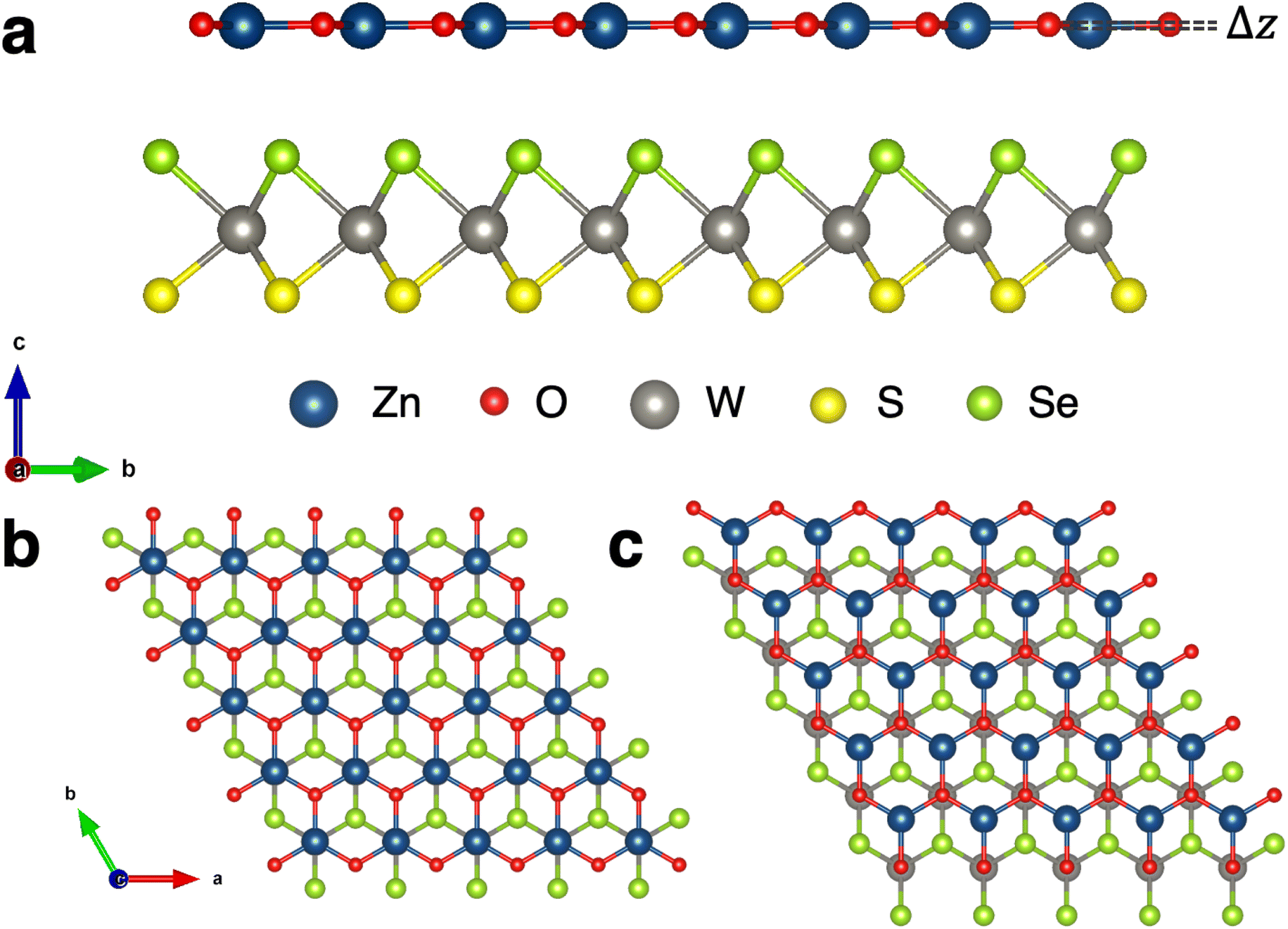 | ||
| Fig. 1 Stacking configurations of Janus WSSe–ZnO heterostructures. (a) Side view with Se on the same side as ZnO (AB-I-Se). The buckling Δz of the ZnO monolayer gives rise to its dipole moment. (b) Top view in type I registry with AB stacking with W and Zn aligned and Se on the same side as ZnO (AB-I-Se). (c) Top view in type II registry with AB stacking with W and O aligned and Se on the same side as ZnO (AB-II-Se). | ||
| Stacking configuration | Binding energy (eV per unit cell) | a-Lattice parameter |
|---|---|---|
| AA-I-Se | −0.217 | 3.255 |
| AA-I-S | −0.202 | 3.255 |
| AA-II-Se | −0.262 | 3.259 |
| AA-II-S | −0.257 | 3.259 |
| AB-I-Se | −0.276 | 3.257 |
| AB-I-S | −0.269 | 3.257 |
| AB-II-Se | −0.277 | 3.257 |
| AB-II-S | −0.260 | 3.257 |
The phonon band structures of each of these three most stable stacking patterns are calculated to determine whether these structures are dynamically stable (Fig. 2). The AB-II-Se stacking pattern exhibits imaginary optical modes and is therefore unstable. The AB-I-S and AB-I-Se stacking patterns do not exhibit any such instabilities so these two structures are selected for further analysis. It should be noted that the binding energy of the AB-II-Se stacking pattern differs from that of AB-I-Se by an extremely minimal amount, ∼1 meV per unit cell or ∼0.2 meV per atom, making them energetically nearly degenerate within the precision of the methods employed in this work. Analysis of the unstable phonon modes near the Brillouin zone center in the phonon band structure of the AB-II-Se structure reveals that they correspond to lateral sliding of the two layers relative to one another.
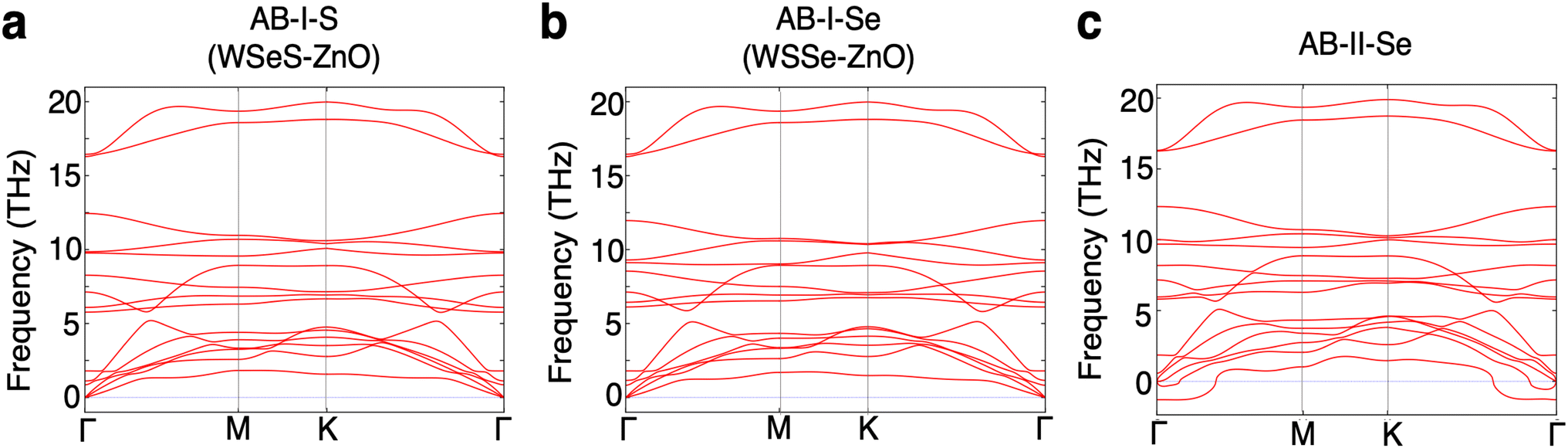 | ||
| Fig. 2 The phonon band structures of the three stacking configurations with the largest binding energies (a) AB-I-S (WSeS–ZnO), (b). AB-I-Se (WSSe–ZnO), and (c) AB-II-Se. AB-II-Se exhibits imaginary optical modes indicating that the structure is not stable. | ||
Effectively, the dynamical instability in the AB-II-Se stacking pattern promotes realignment of the layers into a preferred stacking pattern. Further analysis of energetic barriers to sliding and dynamical instabilities driving sliding in these heterostructures would be a valuable topic for future study.
Going forward, we shall refer to the AB-I-S and AB-I-Se heterostructures as WSeS–ZnO and WSSe–ZnO respectively to make it clear which orientation of WSSe with respect to ZnO we are referring to, with the final chalcogen in the Janus TMD label referring to the chalcogen that faces the ZnO monolayer. Discussion of these heterostructures, without reference to any particular configuration, will be indicated with the term Janus TMD–ZnO for clarity.
The DFT band structures of the WSeS–ZnO and WSSe–ZnO stacking patterns are calculated using HSE06 (Fig. 3b and e) using the crystal structures obtained from structural relaxation using PBE+D3. In all cases the valence band (VB) and conduction band (CB) are dominated by WSSe orbital contributions. The only notable mixing that occurs is in the WSSe–ZnO structure with Se facing ZnO – some hybridization between the two layers occurs in the CB at the Γ point. The band gaps for both structures are direct gaps at K and have the same magnitude as the band gap of monolayer WSSe (Table 2). These heterostructures are computed to have a type I band edge alignment with the ZnO band edges straddling the WSSe band edges.
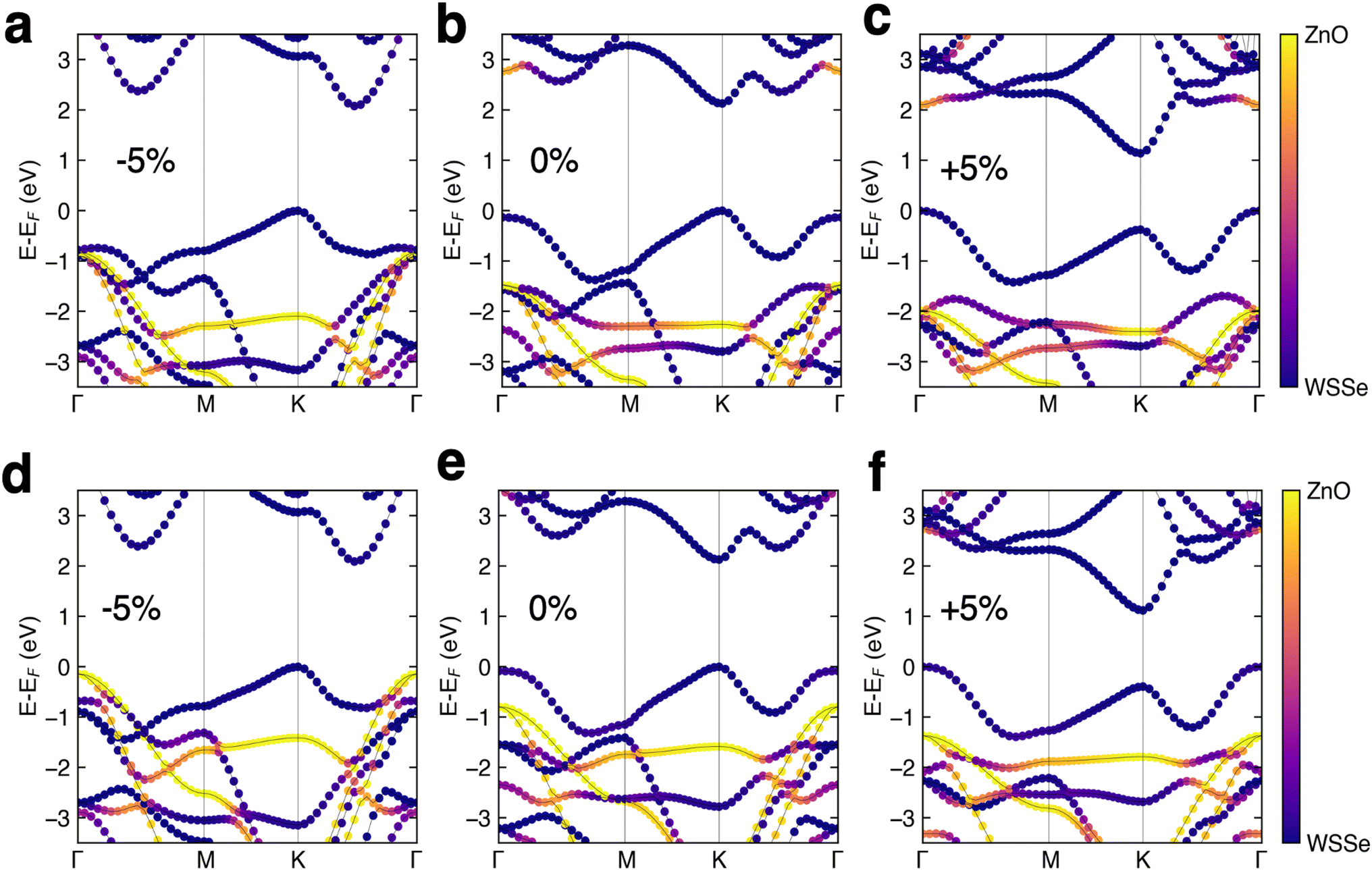 | ||
| Fig. 3 Band structures of the Janus TMD–ZnO heterostructures for WSSe–ZnO (a–c) and WSeS–ZnO (d–f) at 5% compressive strain (a and d), no strain (b and e), and 5% tensile strain (c and f). The orbital projections are color coded so that orbitals with more WSSe character are purple and those with more ZnO character are yellow, as indicated by the color bars. | ||
| Stacking configuration | DFT-HSE band gap (eV) |
|---|---|
| WSSe | 2.14 |
| ZnO | 3.73 |
| WSSe–ZnO | 2.13 |
| WSeS–ZnO | 2.13 |
Prior DFT calculations investigating Janus TMD–ZnO heterostructures using HSE found that the band edges were type I when S faced the ZnO (WSeS–ZnO) but type II when Se faced the ZnO (WSSe–ZnO),33 inconsistent with our results. It should be noted that our calculated PBE band structures of both WSeS–ZnO and WSSe–ZnO exhibit type II alignment, with the VBM dominated by orbitals of ZnO character (ESI Fig. S2†) Our calculated HSE band gap for WSSe is similar to that of the prior work. While our calculated lattice parameters for ZnO are the same as those in this prior work, our converged HSE band gap for ZnO is significantly larger, 3.73 eV versus 3.10 eV, which could explain the discrepancy. The experimental fundamental band gap of monolayer ZnO is 4.48 eV,28 significantly larger than our calculated value of 3.73 eV, making it reasonable to assume that these heterostructures would indeed exhibit type I alignment experimentally.
3.2 In-plane biaxial strain and out-of-plane uniaxial strain
In-plane biaxial strain has been shown in prior work to be a useful knob that can be turned to tune the electronic structure of TMDs.52–56 In 2D materials, strain can be applied in a variety of ways, including by transferring the 2D material to a flexible substrate that can then be bent, to a piezoelectric substrate whose dimensions can be modified with an electric field, or to an array of nanopillars.56 To investigate the effect of in-plane biaxial strain on the Janus TMD–ZnO heterostructures we perform band edge alignment calculations with varying amounts of tensile and compressive biaxial strain, up to 5%, calculating the absolute VBM position relative to vacuum and the band gap using HSE. Experiments have reported that TMDs can withstand large degrees of strain. For example, one experiment used an atomic force microscopy cantilever, reporting that monolayer MoS2 did not break until a strain between 6 and 11% was reached.57 In all cases the heterostructures are fully optimized at the stretched or compressed lattice parameters, with the internal coordinates allowed to relax. In the relaxed structures, a small amount of buckling occurs in the ZnO layer, with the plane of the O atoms ∼ 0.03 Å above the plane of the Zn atoms in the unstrained case (Fig. 4a). The interlayer separation between the topmost chalcogen and the ZnO layer and the bond lengths for the non-strained, largest compressive biaxial strains, and largest tensile biaxial strains are listed in Table 3. In general, the interlayer distance is 0.1 Å larger when Se faces the ZnO layer than when S faces the ZnO layer. The Zn–O, W–Se, and W–S bond lengths increase and decrease comparably for both stacking configurations for biaxial tensile and compressive strain respectively.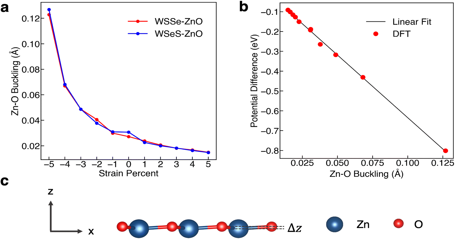 | ||
| Fig. 4 The effect of biaxial in-plane strain on the buckling in monolayer ZnO. (a) Magnitude of the buckling (Δz) in ZnO layer as a function of in-plane biaxial strain for the two heterostructures studied, calculated as the difference between the Cartesian z-position of the O ion and that of the Zn ion. (b) Magnitude of the electrostatic potential energy difference across a monolayer of ZnO for each buckling value and a linear fit (black line). (c) Schematic of the difference of the Cartesian z-positions of the O ion and the Zn ion, with Δz corresponding to the Zn–O buckling values. | ||
| Stacking configuration | Strain (%) | Interlayer distance (Å) | Zn–O bond length (Å) | W–Se bond length (Å) | W–S bond length (Å) | HSE band gap (eV) |
|---|---|---|---|---|---|---|
| WSSe–ZnO | −5 | 3.20 | 1.79 | 2.52 | 2.39 | 2.08 |
| WSSe–ZnO | 0 | 3.08 | 1.88 | 2.54 | 2.42 | 2.13 |
| WSSe–ZnO | 5 | 2.97 | 1.97 | 2.57 | 2.46 | 1.14 |
| WSeS–ZnO | −5 | 3.07 | 1.79 | 2.52 | 2.39 | 2.09 |
| WSeS–ZnO | 0 | 2.96 | 1.88 | 2.54 | 2.43 | 2.13 |
| WSeS–ZnO | 5 | 2.87 | 1.97 | 2.57 | 2.47 | 1.12 |
The degree of buckling of the ZnO monolayer, defined as the difference between the z-position of the O atom and that of the Zn atom, is also a function of biaxial strain percent, with compressive biaxial strain producing a large increase in the buckling and tensile biaxial strain producing a smaller decrease in the buckling (Fig. 4a). At 5% in-plane compressive biaxial strain the buckling in the ZnO layer increases up to more than 0.12 Å while at 5% tensile biaxial strain the ZnO layer buckling decreases to 0.015 Å. We calculate the plane-averaged electrostatic potential energy across the ZnO monolayers alone for different amounts of buckling and find that the potential energy difference scales linearly with the magnitude of the buckling, as expected if the Zn cation and O anion charges were independent of buckling. This indicates that the biaxial in-plane compressive strain is a direct means of tuning the dipole moment of the ZnO monolayer and that it possesses a strong effective piezoelectric response.
The HSE band structures of the strained structures are displayed in Fig. 3. In both stacking configurations tensile biaxial strain decreases the band gap, by ∼1 eV at 5% strain, and makes the gap just barely indirect, with the Γ point in the VB increasing in energy from being 132 meV below the K point to 374 meV above the K point in WSSe–ZnO and from being 83 meV below the K point to 393 meV above the K point in WSeS–ZnO. The K–K transition for WSSe decreases as well by 620 meV at the maximum value of strain explored here. While the dominant contributions to the VBM and CBM in a TMD are generally from Mo or W d orbitals, dxy and dx2−y2 for the VBM at K and dz2 for the CBM at K (ESI Fig. S3a†), this trend can be rationalized in the context of the smaller, but nontrivial, chalcogen p-orbital contributions. These orbital contributions are predominantly in-plane px and py (ESI Fig. S3b†). In a simplified bonding–antibonding orbital picture, the lateral separation between the chalcogens can modulate the K–K transition energy, with closer proximity increasing the K–K gap and larger separation decreasing the K–K gap. Compressive biaxial strain has a significant effect on the CB, with the gap becoming indirect due to a reordering of the relative energies of the K and Λ valleys, where the Λ valley lies along the high symmetry line between the Γ and K valleys. In this case the K–K transition of WSSe increases in energy, consistent with the chalcogen p-orbital rationalization.
A trend emerges in the effect of biaxial strain on the relative alignment of the WSSe and ZnO band edges. Tensile biaxial strain tends to shift the ZnO bands to lower energy relative to those of WSSe whereas compressive biaxial strain tends to shift the ZnO bands to higher energy. Under compressive strain the WSSe band gap does not change and the shifts in WSSe band energies are attributed to the change in the buckling of the ZnO layer under biaxial compressive strain (Fig. 4). The buckling and the magnitude of the ZnO layer's associated dipole moment, driven by biaxial compressive strain, alters the difference in the electrostatic potential on either side of the ZnO monolayer, as seen in Fig. 4b and 6a. Under tensile biaxial strain two concurrent effects occur. First, the buckling in the ZnO and the resulting magnitude of the dipole moment decreases (albeit to a much smaller degree) which is the opposite of the effect seen under compressive biaxial strain (Fig. 3c and f) the absolute positions of the VBM of WSSe are renormalized to slightly higher energies. Overall this manifests as a downward shift in the ZnO VBM energy relative to that of WSSe.
At 5% compressive biaxial strain the ZnO states at the Γ point shift up in energy sufficiently to make the WSeS–ZnO heterostructure a nearly type II heterojunction (Fig. 3d). As our HSE band gap for ZnO is known to be a significant underestimation and it is not known if the error is primarily in the VBM or CBM energy (or both), we cannot conclude that 5% compressive biaxial strain is sufficient to drive a transition to a type II heterojunction. However, we can conclude that under some sufficient, but unknown, amount of compressive biaxial strain, a type II heterojunction could be realized, assuming that the strain were not so large as to destabilize the heterostructure.
The calculated band edge energies for each structure are reported in Fig. 5, in addition to the calculated band edges for monolayer WSSe for comparison. Due to the out-of-plane dipole moment of WSSe the band edge energies are different on opposing sides of the monolayer WSSe and the heterostructures, with the Se side having a smaller work function than the S side. The work functions on either side of the heterostructures are reported separately. Both sides of monolayer WSSe behave similarly under application of biaxial strain (Fig. 5a and b). The VBM increases in energy slightly and the CBM decreases in energy significantly with the application of tensile biaxial strain due to the reduction of the band gap, as has been observed in TMDs under tensile biaxial strain experimentally.53 In the picture described above, in which bonding–antibonding behavior of the chalcogen p-orbitals plays a role in modulating the K–K transition as a function of separation between p-orbitals, it is reasonable that the CBM at K is more strongly affected by tensile strain because the p-orbitals are the only in-plane orbitals (the W orbitals are out-of-plane dz2 orbitals). In the VBM at K however the in-plane character of the W orbitals, which are midway between the chalcogen orbitals, helps mitigate the magnitude of this effect by providing a means by which in-plane orbital hybridization may still occur. This behavior is reproduced in the Janus TMD–ZnO heterostructures on the WSSe sides of the heterostructures (Fig. 5e and h). However, on the ZnO side of the heterostructures the VBM is strongly affected by compressive biaxial strain and decreases dramatically. As the band gap does not change significantly, the CBM decreases in energy correspondingly (Fig. 5d and g). This behavior differs substantially from that of monolayer WSSe and can be attributed to the buckling of the ZnO monolayer and associated increase in its out-of-plane dipole moment.
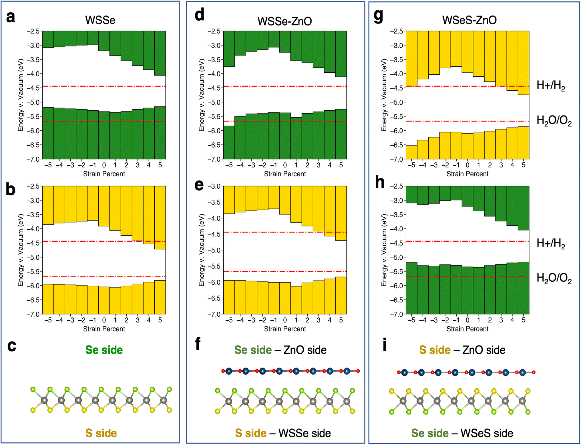 | ||
| Fig. 5 Schematics of band edge alignments under in-plane biaxial strain. Band edge alignment of monolayer WSSe on the (a) Se side and (b) the S side. Band edge alignment of WSSe–ZnO on the (d) Se/ZnO side and (e) S/WSSe side. Band edge alignment of WSeS–ZnO on the (g) S/ZnO side and (h) Se/WSSe side. Schematics of (c) monolayer WSSe, (f) WSSe–ZnO and (i) WSeS–ZnO with labels indicating what Se side, S side, ZnO side and WSSe side refer to. Green or yellow bars indicate that the band edges are calculated from the electrostatic potential relative to the vacuum level on the Se side or S side of WSSe respectively. The redox potentials for the hydrogen evolution reaction and the oxygen evolution reaction at pH = 0 are indicated in red lines. The potentials for pH = 7 and pH = 14 are shown in the ESI (Fig. S7†). | ||
As mentioned, Janus TMDs exhibit an out-of-plane dipole moment due to the differing chalcogen ions on either side. This produces a potential energy difference of 0.71 eV across the monolayer WSSe in our calculations. In the absence of ZnO, the potential energy difference across the WSSe exhibits minimal variation with compressive and tensile biaxial strain (Fig. 6a). Due to the small amount of buckling, monolayer ZnO also experiences a smaller out-of-plane potential energy difference, 0.19 eV in the unstrained structure. However, unlike monolayer WSSe, the magnitude of the potential energy difference of monolayer ZnO is sensitive to compressive biaxial strain and increases dramatically with increasing compressive biaxial strain, up to 0.8 eV at 5% compressive biaxial strain (Fig. 4b and 6a).
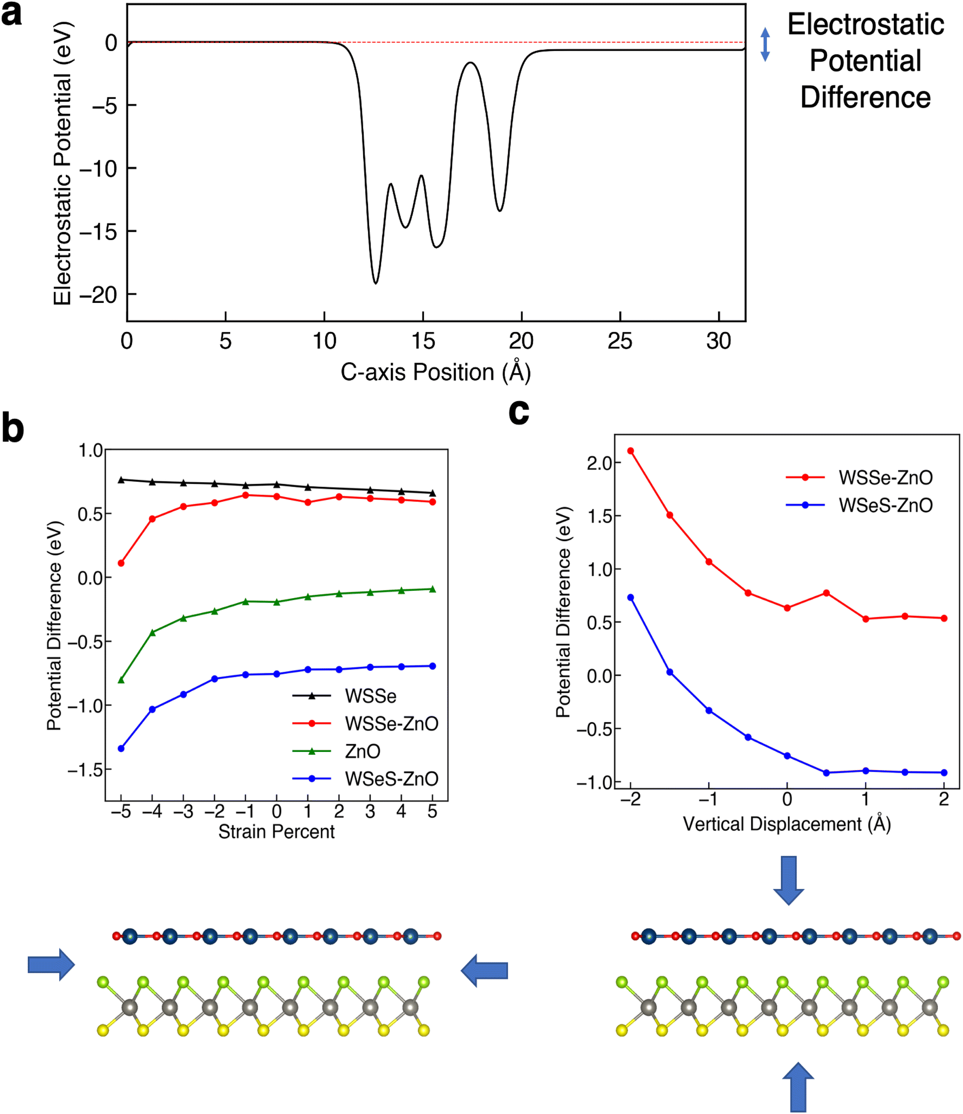 | ||
| Fig. 6 Electrostatic potential differences across WSSe, ZnO, and the heterostructures under study. (a) Plane-averaged electrostatic potential energy along the c-axis of WSSe–ZnO with potential difference indicated on the right hand side with an arrow illustrating the net dipole moment across the heterostructure. (b) The electrostatic potential difference between the ZnO (or top) side and WSSe (or bottom) side of monolayer WSSe, monolayer ZnO, and the two most stable stacking configurations WSSe–ZnO and WSeS–ZnO. Compressive strain tends to make the electrostatic potential difference more negative. (c) The electrostatic potential difference between the ZnO side and WSSe side of the two most stable stacking configurations as a function of displacement of the ZnO from the equilibrium separation. Vertical compression tends to make the electrostatic potential difference more positive. | ||
In all of the heterostructures studied, the buckling in the ZnO layer has the same directionality, with O shifted slightly higher and further away from the TMD than Zn, irrespective of biaxial strain percent. However, the sign of the potential energy difference in the WSSe layer is reversed depending on which chalcogen faces the ZnO layer. The electrostatic potential of the S side of WSSe is always at lower (more negative) energy than the Se side. The sign of the electrostatic potential energy difference, meaning whether the top or bottom is at higher potential energy, is the same for ZnO and WSSe in the WSeS–ZnO configuration, but is opposite in the WSSe–ZnO configuration. In this discussion top and bottom are referenced to the orientation displayed in Fig. 1a where ZnO is on top of the Janus TMD. As compressive biaxial strain is applied, the electrostatic potential difference between the ZnO side and WSSe side of both WSSe–ZnO and WSeS–ZnO becomes more negative, mimicking the trend for the electrostatic potential difference of the ZnO (Fig. 6a). If the ZnO monolayer were inverted, with O in closer proximity to the WSSe and the dipole moment of the ZnO reversed, we expect that the opposite effect would occur, with the potential difference across the ZnO becoming more positive and the bands of the heterostructures shifting to higher energies under compressive in-plane biaxial strain.
Further insight can be gained by considering the effects of vertical proximity via out-of-plane uniaxial strain. From Table 3, compressive biaxial strain moves the ZnO layer further away from the WSSe and tensile biaxial strain moves the ZnO layer closer. To investigate the effects of out-of-plane uniaxial strain, band edge calculations are performed on the unstrained structures with the ZnO layer moved closer and farther away from the WSSe. The effect of vertical displacement on the band edge energies, defined as the deviation of the interlayer spacing from the equilibrium distance of each structure, is displayed in Fig. 7. The electrostatic potential energy of the WSSe side is not affected by the changing vertical proximity. However, the electrostatic potential on the ZnO side of the heterostructure is strongly affected by decreasing interlayer separation. The electrostatic potential energy difference between the ZnO side and the WSSe side of each heterostructure becomes more positive with decreasing interlayer separation (Fig. 6b). Further, as the vertical separation decreases, the VB edges of the Janus TMD–ZnO heterostructures on the ZnO side of the heterostructure shift to higher energies, the opposite of the effect exhibited under in-plane biaxial compression.
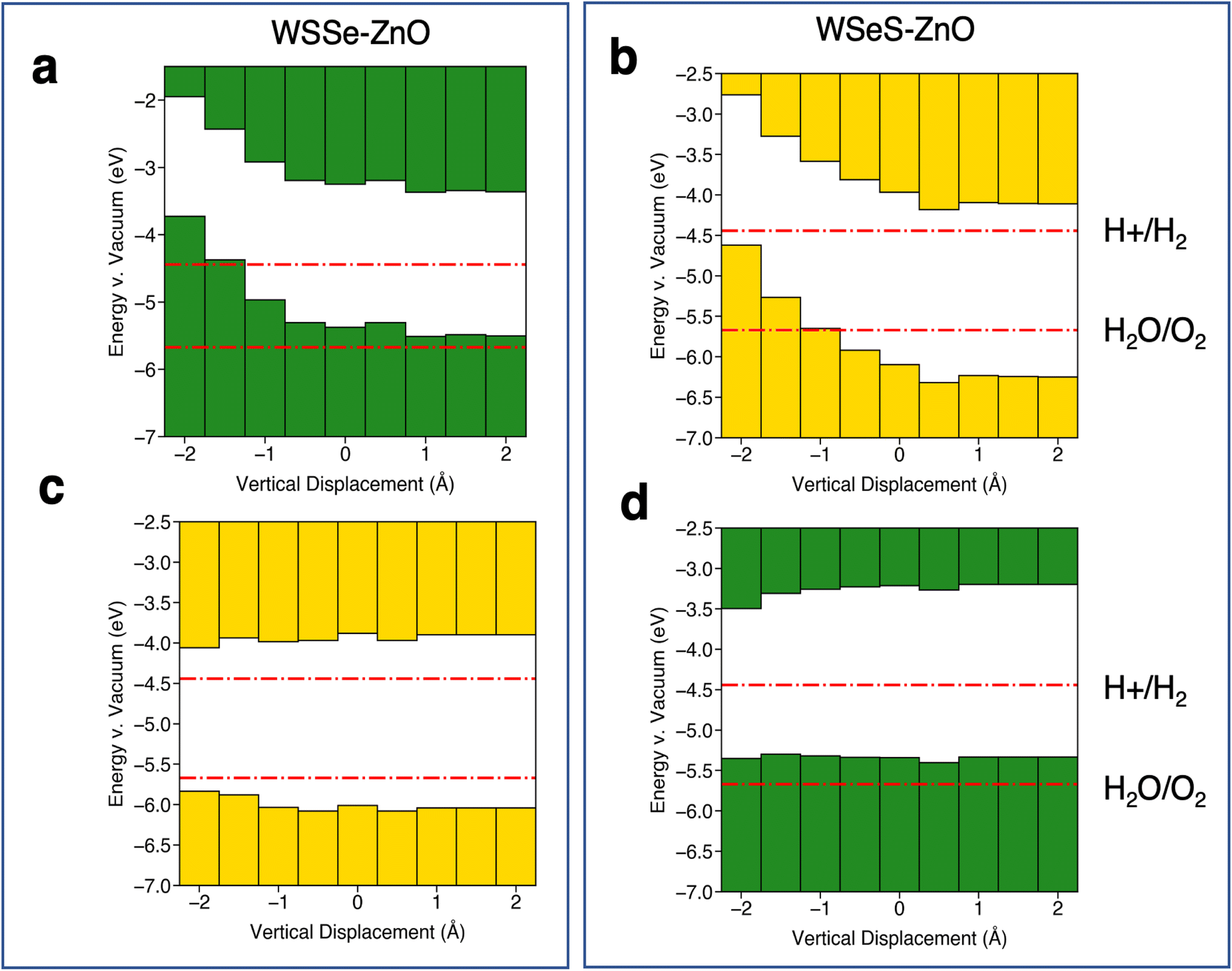 | ||
| Fig. 7 Summaries of band edge alignments under out-of-plane uniaxial strain. Band edge alignment of the most stable stacking configurations on the ZnO side of the heterostructure (a and b) and the WSSe side of the heterostructure (c and d) for (a and c) WSSe–ZnO and (b and d) WSeS–ZnO as a function of the vertical displacement of the ZnO relative to the equilibrium separation of ZnO and WSSe in each heterostructure. ZnO side and WSSe side are defined as in Fig. 5f and i. Green or yellow bars indicate that the band edges are calculated from the electrostatic potential relative to the vacuum level on the Se side or S side of WSSe respectively. The redox potentials for the hydrogen evolution reaction and the oxygen evolution reaction at pH = 0 are indicated in red lines. The potentials for pH = 7 and pH = 14 are shown in the ESI (Fig. S8†). | ||
A significant energetic barrier exists for large amounts of vertical compression (ESI Fig. S6†), however even with small amounts of vertical compression a substantial change in the band edge energies can be observed. For example, in the WSeS–ZnO heterostructure a decrease in the vertical separation of 0.5 Å can generate a 177 meV shift in the valence band edge with an energy cost of 23 meV per atom, on the order of thermal energies expected at room temperature.
This work demonstrates that the band edge energies of the Janus TMD–ZnO heterostructure can be shifted to lower energies with compressive in-plane biaxial strain or shifted to higher energies with compressive out-of-plane uniaxial strain. Moreover, ZnO plays a large role in determining the band edge energies of these heterostructures even though, in our calculations, its band edges straddle those of WSSe and do not make large orbital contribution to the heterostructures' VB and CB edges. The interplay between the dipole moment of ZnO and that of WSSe is critical in producing this phenomenon as it does not occur in monolayer WSSe alone, as demonstrated by the lack of change in the electrostatic potential energy difference across WSSe (Fig. 6a) and the lack of a downward shift in the VBM position under compressive in-plane biaxial strain (Fig. 5a and b) for isolated monolayer WSSe. A similar effect has been observed in multilayer MoSSe, with the dipole moments of successive layers inducing shifts in the band edges on either side of the multilayer structure,12 indicating that band edge control via tunable monolayer dipole moments has more general implications for the functionality of vdW heterostructures, beyond our calculations here.
For completeness, we calculate the phonon band structures of the Janus TMD–ZnO heterostructures under compressive in-plane biaxial and compressive out-of-plane uniaxial strain. Under compressive in-plane biaxial strain the heterostructures begin to exhibit imaginary frequency phonon modes indicating dynamical instability (ESI Fig. S4†). The imaginary phonon modes are confined to the ZnO layer indicating that ZnO may undergo a phase transition upon application of compressive in-plane biaxial strain. While prior first-principles work studying ZnO under biaxial strain has been performed and the tunability of the electronic structure under these conditions has been reported,25,26 it appears that the dynamical and phase stability of this material under biaxial strain have not yet been studied in detail. The phonon modes at imaginary frequencies are localized in the ZnO layer and the eigenvectors correspond to alternating out-of-plane displacements, suggesting that a phase transition could occur to a buckled structure with periodic oscillations of the directionality of the buckling and dipole moments. This would likely diminish the magnitude of the band edge tuning effect. Encouragingly though, small amounts of compressive out-of-plane uniaxial strain, such as the likely energetically-achievable decrease in vertical separation of 0.5 Å, do not produce imaginary phonon frequencies, although large amounts of compression do (ESI Fig. S5†). We note that our phonon calculations are limited to the harmonic approximation at zero temperature which does not always reflect dynamical stability at finite temperature, such as the bcc high-temperature phase of many metals.58 Despite the calculated dynamical instability of ZnO under compressive in-plane biaxial strain, we continue the discussion of the properties of these heterostructures under varying degrees and types of strain as our calculations do not rule out the possibility of dynamical stability at finite temperature and, moreover, our results should be generalizable to heterostructures of Janus TMDs and other 2D materials that have small out-of-plane dipole moments and hence are still of value in a broader discussion of engineering novel vdW heterostructures for photocatalytic and other optoelectronic applications.
3.3 Electric field
Application of an out-of-plane electric field, for example via an underlying gate or in a sandwich geometry via electrodes, is another method for tuning electronic structure. In prior first-principles work it has been shown that an out-of-plane electric field does not substantially affect the band gap of monolayer Janus TMDs.11 Past work on the effect of out-of-plane electric fields on TMD homobilayers however suggests that application of an electric field can substantially change the band gap, producing a transition to a metallic state near 0.5–1.0 eV Å−1.59 As the heterostructures under study in this work are heterobilayers, we perform band structure calculations to determine whether an out-of-plane electric field will affect the Janus TMD–ZnO heterostructures as though they were Janus TMD monolayers or as though they were TMD homobilayers.We calculate the HSE band structures of our two stacking configurations under the application of out-of-plane electric fields of varying strengths. From our DFT calculations, we find that application of an out-of-plane electric field substantially affects the magnitude of the buckling in the ZnO by ∼0.08 Å per 1 eV Å−1 applied field, even inverting the ZnO buckling when a sufficiently strong electric field in the negative z direction is applied. However, an out-of-plane electric field does not change the band gap of these heterostructures by more than 0.01 eV, both at moderate and very large electric field strengths up to 1 eV Å−1 and both with and without geometric relaxation (ESI Table S1†). This is reasonable given that the valence and conduction band edges are dominated by WSSe states, with the ZnO valence and conduction band edges straddling those of WSSe. Effectively, the band edges of the Janus TMD–ZnO heterostructure behave as though the system were a Janus TMD monolayer in the presence of an out-of-plane electric field. The relative alignment of the ZnO bands to those of WSSe shift to lower energies and higher energies with application of electric fields up to 1 eV Å−1 oriented in the negative z and positive z directions respectively, however not to a sufficient degree to produce a type II heterojunction (ESI Fig. S9–S11†).
With respect to the absolute band edge energies of the Janus TMD–ZnO heterostructures, calculation of the absolute VBM position via the electrostatic potential is challenged by the fact that the electrostatic potential in the vacuum region is not constant in the presence of an electric field and there is no well-defined vacuum energy. However, in prior work it has been shown that monolayer TMDs stacked on ferroelectric materials experience shifts in their work function as a result of proximity to an out-of-plane electric polarization.60 For example, monolayer MoS2 stacked on BiFeO3 with a fixed out-of-plane polarization experiences rigid shifts in its band edges, to lower energy and higher energy in the presence of a positive or negative BiFeO3 surface polarization, which can be patterned to produce p–n junctions between regions of ferroelectric domains with opposite polarization.9 This indicates that it may be possible to tune the band edges of the Janus TMD–ZnO heterostructures rigidly with an out-of-plane electric field, or a substrate with a finite out-of-plane electric polarization. The magnitude of the buckling in the Zn–O layer varies with electric field strength as well (ESI Table S1†) which is also expected to shift the band edges, as observed in the case of in-plane biaxial strain. Electric fields oriented in the positive z direction increase the Zn–O buckling, which in our in-plane biaxial strain calculations corresponds to a downward shift of the heterostructure band edges to lower energies. From the MoS2–BiFeO3 results in prior work,9 an electric field in the positive z direction would also be expected to produce a downward shift of the band edges to lower energies. This indicates that an applied electric field, or a substrate with a finite out-of-plane electric polarization work in tandem with the dipole moment of ZnO to amplify the magnitude of the band edge energy shifts that would be expected to be produced by each of them independently.
3.4 Relevance of Janus WSSe–ZnO heterostructures for photocatalytic applications
For photocatalytic (and electrocatalytic) applications the absolute positions of the band edges relative to the redox potentials of the water splitting reaction or CO2RR are critical. In much of the past experimental work considering TMD photocatalysts attention has been paid primarily to using TMDs as cathodes for the relevant reduction reactions (HER and CO2RR)3–5 rather than acting as a catalyst for the entire water splitting reaction, donating both holes and electrons for OER and HER. Leveraging control over the CB energies has been studied as a means of attempting to tune product selectivity amongst the various competing CO2RR products and HER.6 Nonetheless, it is still informative to consider the band edges of the Janus TMD–ZnO heterostructures relative to both the OER and HER, knowing that the CO2RR potentials are in the neighborhood of the HER potentials.1,2The redox potentials for the hydrogen evolution reaction (HER) and oxygen evolution reaction (OER) at pH = 0 are plotted on the band edge plots in Fig. 5 and 7. It is important to note that under operating conditions in aqueous environment the relative positions of the HER and OER redox potentials to the band edges of the heterostructures will differ from the relative positions of the pH = 0 redox potentials to those of the vacuum band edges of the heterostructures. First, the dipole moments of the water molecules on the surface of the heterostructure will alter the relative alignment. Second, the HER and OER redox potentials are functions of pH and shift according to the Nernst equation (eqn (2))61 as pH is increased to more realistic operating conditions, that is
| E(pH) = E(pH = 0) + 0.0591 × pH, | (2) |
Another consideration is Pourbaix stability, or the stability of a material under aqueous conditions and applied bias. Using the Materials Project Pourbaix Diagram software,63–66 the most energetically stable species (including both solids and ions) for a given elemental composition at a particular pH and applied potential can be determined, as well as the energy above hull for unstable species. Neither WSSe nor monolayer ZnO are the most stable species at any pH or applied potential. For example, at pH = 7 and no bias voltage relative to the reversible hydrogen electrode (RHE), the potential corresponding to HER, WSSe is 0.10 eV per atom above the Pourbaix hull and monolayer ZnO is 0.39 eV per atom above the Pourbaix hull. At a bias voltage of −0.5 V vs. RHE, a representative value considered in prior work to correspond to reducing conditions for CO2RR,19 the energies above hull are 0.29 eV per atom and 0.39 eV per atom respectively. Past work comparing the calculated energy above the Pourbaix hull for a number of known oxide photoanode materials, however, found that many of them exhibited a nonzero energy above hull, up to 0.5 eV per atom.65 The experimentally observed stability of these materials was attributed to kinetic barriers to undergoing a phase transition to the more stable phase. While this does not guarantee that the Janus TMD–ZnO heterostructures studied here will also exhibit this meta-stability, it cannot be ruled out that they may exhibit operational stability. Alternatively, addition of an encapsulating protective coating of a Pourbaix stable 2D material or thin film could be employed to protect the heterostructures.
The relative alignment of the band edges of the heterostructures to the HER and OER potentials at pH = 0, 7, and 14 are plotted in the ESI in Fig. S7 and S8.† In general, due to the electrostatic potential energy difference between the Se and S sides of WSSe, the band edges on the side of the heterostructure that the Se faces will always be at higher energy. The VBM is generally ∼0.7 eV higher in energy on the Se side (Fig. 5a, d and h). The HER and OER redox potentials increase in energy by ∼0.4 eV at pH = 7 according to the Nernst equation, in which case the Se sides of the heterostructures are more likely to straddle the band edges. Thus, the large dipole moment across the Janus TMD–ZnO heterostructures allows for the band edges to straddle the HER and OER potential at the redox potentials corresponding to a variety of pHs by varying which side of the heterostructure is used as the catalytic surface (i.e. the side of the heterostructure from which photoexcited carriers would be donated to catalyze chemical reactions) and the amount of strain applied.
Relative to the redox potentials under extreme acidic conditions (pH = 0) the WSSe side of the WSSe–ZnO heterostructure is terminated by S ions making that side optimal for a catalytic surface (Fig. 5e). Alternatively, using the ZnO as the catalytic surface, the S side of WSeS–ZnO under no strain (Fig. 5g) or the Se side of WSSe–ZnO with the application of compressive biaxial strain (Fig. 5d) would be appropriate. Relative to the redox potentials under neutral conditions (pH = 7), both the S terminated side of WSSe–ZnO (Fig. 5e) and the Se terminated side of WSeS–ZnO (Fig. 5h) could have appropriate band edge positions. Relative to the redox potentials under extreme basic conditions (pH = 14) the WSSe side of the WSeS–ZnO heterostructure is terminated by Se ions making the band edges of that side of this stacking configuration likely the best candidate for a photocatalytic surface (Fig. 5h). Using ZnO as the catalytically active surface, the Se side of WSSe–ZnO under no strain (Fig. 5d) or the ZnO sides of WSeS–ZnO and WSSe–ZnO under the application of compressive out-of-plane uniaxial strain (Fig. 7a and b) could be suitable. As we expect the PZC of these heterostructures to be at pHs higher than pH = 0, it is encouraging that the dynamically unstable heterostructures under compressive biaxial strain are perhaps not the most relevant for photocatalytic applications. The heterostructures that best straddle the pH = 7 and pH = 14 redox potentials exhibit dynamical stability, with no imaginary phonon modes.
In the cases in which the ZnO side of the heterostructure is used as the catalytic surface, carriers would need to tunnel through to the ZnO layer since the VBM and CBM are dominated by WSSe orbitals (Fig. 3) and excited carriers would be expected to reside in the WSSe layer. In WSSe–ZnO under zero or tensile biaxial strain our HSE band structure calculations indicate that the CB is characterized by hybridization of WSSe and ZnO states at the Γ point that are nearly degenerate with the CBM at the K point enhancing the probability for electron tunneling to the ZnO layer. Similarly, for the WSeS–ZnO heterostructure, under biaxial compressive strain our HSE band structure calculations indicate that the VB is characterized by ZnO states at the Γ point that are nearly degenerate with the VBM at K making it favorable for holes to tunnel to the ZnO layer. Preventing charge recombination is critical to efficient photocatalysis so if this tunneling or hopping could be achieved the photocatalytic efficiency of these heterostructures would be significantly enhanced.
4 Conclusions
DFT calculations on Janus WSSe–ZnO heterostructures are performed to study the effects of in-plane biaxial strain, out-of-plane uniaxial strain, and electric field on the electronic structure of these heterostructures, demonstrating the tunability of their electronic properties. In particular, the buckling of the ZnO monolayer and its associated dipole moment can be significantly altered with compressive biaxial strain or uniaxial strain, providing a knob for tuning the band edge energies of the heterostructure on its ZnO side.Our investigation demonstrates that the band gaps and absolute band edge energies of vdW heterostructures of 2D materials with finite dipole moments can be tuned by the application of strain when the magnitude of the dipole moment of one of the layers is correspondingly tuned by strain. The significance of this result is that a single heterostructure, with a clean vdW interface, could be synthesized and mechanically manipulated to tune its band edges. This differs from prior studies of band edge tuning via changing the elemental composition or constructing interfaces with or passivating surfaces of bulk materials, that suffer from less controllable effects like surface or interfacial reconstruction. This effect should be generalizable to other vdW heterostructures and could potentially be harnessed for the development of novel photocatalysts with tunable band edge energies.
Conflicts of interest
We have no conflicts of interest to disclose.Acknowledgements
This work is supported in part by the Liquid Sunlight Alliance through the U.S. Department of Energy, Office of Science, Office of Basic Energy Sciences, Fuels from Sunlight Hub under award number DE-SC0021266. Additional funding was provided by the Kavli Energy Nanosciences Institute at the University of California Berkeley through the Graduate Student Philomathia Fellowship. This work was also partially supported by funding provided by Addis Ababa University under thematic project (grant no. RD/LT-095/2019). This collaborative effort resulted from the American Physical Society's US Africa Initiative, an APS Innovation Fund. This research used computing resources from the Lawrencium computational cluster resource provided by the IT Division at the Lawrence Berkeley National Laboratory, supported by the Director, Office of Science, Office of Basic Energy Sciences, of the U.S. Department of Energy under contract no. DE-AC02-05CH11231.Notes and references
- Y. Izumi, Coord. Chem. Rev., 2013, 257, 171–186 CrossRef CAS.
- F. Haque, T. Daeneke, K. Kalantar-zadeh and J. Z. Ou, Nano-Micro Lett., 2018, 10, 23 CrossRef.
- H. Wang, C. Tsai, D. Kong, K. Chan, F. Abild-Pedersen, J. K. Nørskov and Y. Cui, Nano Res., 2015, 8, 566–575 CrossRef CAS.
- G. Li, D. Zhang, Q. Qiao, Y. Yu, D. Peterson, A. Zafar, R. Kumar, S. Curtarolo, F. Hunte, S. Shannon, Y. Zhu, W. Yang and L. Cao, J. Am. Chem. Soc., 2016, 138, 16632–16638 CrossRef CAS.
- M. Asadi, B. Kumar, A. Behranginia, B. A. Rosen, A. Baskin, N. Repnin, D. Pisasale, P. Phillips, W. Zhu, R. Haasch, R. F. Klie, P. Král, J. Abiade and A. Salehi-Khojin, Nat. Commun., 2014, 5, 4470 CrossRef CAS PubMed.
- Y.-R. Lin, W.-H. Cheng, M. H. Richter, J. S. DuChene, E. A. Peterson, C. M. Went, Z. Y. Al Balushi, D. Jariwala, J. B. Neaton, L.-C. Chen and H. A. Atwater, J. Phys. Chem. C, 2020, 124, 22893–22902 CrossRef CAS.
- M. H. Richter, E. A. Peterson, L. Zhou, A. A. Shinde, P. F. Newhouse, Q. Yan, S. W. Fackler, J. Yano, J. K. Cooper, K. A. Persson, J. B. Neaton and J. M. Gregoire, Chem. Mater., 2021, 33, 7242–7253 CrossRef CAS.
- S. Yang, D. Prendergast and J. B. Neaton, Nano Lett., 2012, 12, 383–388 CrossRef CAS.
- J.-Q. Dai, X.-W. Wang and T.-F. Cao, J. Phys. Chem. C, 2019, 123, 3039–3047 CrossRef CAS.
- A. Geim and I. Grigorieva, Nature, 2013, 499, 419–425 CrossRef CAS.
- Q.-F. Yao, J. Cai, W.-Y. Tong, S.-J. Gong, J.-Q. Wang, X. Wan, C.-G. Duan and J. H. Chu, Phys. Rev. B, 2017, 95, 165401 CrossRef.
- A. C. Riis-Jensen, M. Pandey and K. S. Thygesen, J. Phys. Chem. C, 2018, 122, 24520–24526 CrossRef CAS.
- A.-Y. Lu, H. Zhu, C.-P. Chuu, Y. Han, M.-H. Chiu, C. C. Cheng, C.-W. Yang, K.-H. Wei, Y. Yang, Y. Wang, D. Sokaras, D. Nordlund, P. Yang, D. A. Muller, M.-Y. Chou, X. Zhang and L.-J. Li, Nat. Nanotechnol., 2017, 12, 744–749 CrossRef CAS.
- J. Zhang, S. Jia, I. Kholmanov, L. Dong, D. Er, W. Chen, H. Guo, Z. Jin, V. B. Shenoy, L. Shi and J. Lou, ACS Nano, 2017, 11, 8192–8198 CrossRef CAS PubMed.
- Y. C. Cheng, Z. Y. Zhu, M. Tahir and U. Schwingenschlögl, Europhys. Lett., 2013, 102, 57001 CrossRef.
- L. Dong, J. Lou and V. B. Shenoy, ACS Nano, 2017, 11, 8242–8248 CrossRef CAS PubMed.
- Y. Liang, J. Li, H. Jin, B. Huang and Y. Dai, J. Phys. Chem. Lett., 2018, 9, 2797–2802 CrossRef CAS.
- C. Long, Y. Dai, Z.-R. Gong and H. Jin, Phys. Rev. B, 2019, 99, 115316 CrossRef CAS.
- A. K. Singh, J. H. Montoya, J. M. Gregoire and K. A. Persson, Nat. Commun., 2019, 10, 443 CrossRef CAS.
- Z. Zhou, X. Niu, Y. Zhang and J. Wang, J. Mater. Chem. A, 2019, 7, 21835–21842 RSC.
- C. Tusche, H. L. Meyerheim and J. Kirschner, Phys. Rev. Lett., 2007, 99, 026102 CrossRef CAS.
- J. Yuhara, D. Kato, T. Matsui and S. Mizuno, J. Chem. Phys., 2015, 143, 174701 CrossRef CAS.
- H. T. Quang, A. Bachmatiuk, A. Dianat, F. Ortmann, J. Zhao, J. H. Warner, J. Eckert, G. Cunniberti and M. H. Rümmeli, ACS Nano, 2015, 9, 11408–11413 CrossRef CAS.
- H.-K. Hong, J. Jo, D. Hwang, J. Lee, N. Y. Kim, S. Son, J. H. Kim, M.-J. Jin, Y. C. Jun, R. Erni, S. K. Kwak, J.-W. Yoo and Z. Lee, Nano Lett., 2017, 17, 120–127 CrossRef CAS.
- C. Wang, S. Wang, S. Li, P. Zhou, J. Liang and H. Wang, J. Supercond. Novel Magn., 2022, 35, 925–934 CrossRef CAS.
- Y. Miao, Z. Wang, H. Zhao, Q. Chen, H. Wang, M. Wan, L. Chen, K. He and Q. Wang, Mater. Sci. Eng., B, 2020, 254, 114517 CrossRef CAS.
- C. Tan, D. Sun, D. Xu, X. Tian and Y. Huang, Ceram. Int., 2016, 42, 10997–11002 CrossRef CAS.
- J. Lee, D. C. Sorescu and X. Deng, J. Phys. Chem. Lett., 2016, 7, 1335–1340 CrossRef CAS PubMed.
- T.-N. Do, M. Idrees, N. T. T. Binh, H. V. Phuc, N. N. Hieu, L. T. Hoa, B. Amin and H. Van, RSC Adv., 2020, 10, 44545–44550 RSC.
- S. Ahmad, M. Idrees, F. Khan, C. V. Nguyen, I. Ahmad and B. Amin, Chem. Phys. Lett., 2021, 776, 138689 CrossRef CAS.
- L. Zhou, A. Shinde, S. K. Suram, H. S. Stein, S. R. Bauers, A. Zakutayev, J. S. DuChene, G. Liu, E. A. Peterson, J. B. Neaton and J. M. Gregoire, ACS Energy Lett., 2018, 3, 2769–2774 CrossRef CAS.
- J. Kang, S. Tongay, J. Zhou, J. Li and J. Wu, Appl. Phys. Lett., 2013, 102, 012111 CrossRef.
- M. Idrees, H. U. Din, S. U. Rehman, M. Shafiq, Y. Saeed, H. D. Bui, C. V. Nguyen and B. Amin, Phys. Chem. Chem. Phys., 2020, 22, 10351–10359 RSC.
- P. Wang, Y. Zong, H. Liu, H. Wen, Y. Liu, H.-B. Wu and J.-B. Xia, Phys. Chem. Chem. Phys., 2021, 23, 1510–1519 RSC.
- G. Kresse and D. Joubert, Phys. Rev. B: Condens. Matter Mater. Phys., 1999, 59, 1758–1775 CrossRef CAS.
- G. Kresse and J. Furthmüller, Comput. Mater. Sci., 1996, 6, 15–50 CrossRef CAS.
- G. Kresse and J. Furthmüller, Phys. Rev. B: Condens. Matter Mater. Phys., 1996, 54, 11169–11186 CrossRef CAS.
- J. P. Perdew, K. Burke and M. Ernzerhof, Phys. Rev. Lett., 1996, 77, 3865–3868 CrossRef CAS.
- S. Grimme, J. Antony, S. Ehrlich and H. Krieg, J. Chem. Phys., 2010, 132, 154104 CrossRef PubMed.
- M. Topsakal, S. Cahangirov, E. Bekaroglu and S. Ciraci, Phys. Rev. B: Condens. Matter Mater. Phys., 2009, 80, 235119 CrossRef.
- J. Guo, C. Ke, Y. Wu and J. Kang, Nanoscale Res. Lett., 2020, 15, 97 CrossRef CAS.
- J. Heyd, G. E. Scuseria and M. Ernzerhof, J. Chem. Phys., 2003, 118, 8207–8215 CrossRef CAS.
- A. V. Krukau, O. A. Vydrov, A. F. Izmaylov and G. E. Scuseria, J. Chem. Phys., 2006, 125, 224106 CrossRef.
- P. G. Moses, M. Miao, Q. Yan and C. G. Van de Walle, J. Chem. Phys., 2011, 134, 084703 CrossRef PubMed.
- S. De Waele, K. Lejaeghere, M. Sluydts and S. Cottenier, Phys. Rev. B, 2016, 94, 235418 CrossRef.
- M. S. Hybertsen and S. G. Louie, Phys. Rev. Lett., 1985, 55, 1418–1421 CrossRef CAS.
- M. S. Hybertsen and S. G. Louie, Phys. Rev. B: Condens. Matter Mater. Phys., 1986, 34, 5390–5413 CrossRef CAS.
- D. Y. Qiu, F. H. da Jornada and S. G. Louie, Phys. Rev. Lett., 2013, 111, 216805 CrossRef.
- T. A. Pham, D. Lee, E. Schwegler and G. Galli, J. Am. Chem. Soc., 2014, 136, 17071–17077 CrossRef CAS.
- Y. Ping and G. Galli, J. Phys. Chem. C, 2014, 118, 6019–6028 CrossRef CAS.
- A. Togo and I. Tanaka, Scr. Mater., 2015, 108, 1–5 CrossRef CAS.
- A. Castellanos-Gomez, R. Roldán, E. Cappelluti, M. Buscema, F. Guinea, H. S. J. van der Zant and G. A. Steele, Nano Lett., 2013, 13, 5361–5366 CrossRef CAS PubMed.
- D. Lloyd, X. Liu, J. W. Christopher, L. Cantley, A. Wadehra, B. L. Kim, B. B. Goldberg, A. K. Swan and J. S. Bunch, Nano Lett., 2016, 16, 5836–5841 CrossRef CAS PubMed.
- C. V. Nguyen, V. V. Ilyasov, H. V. Nguyen and H. N. Nguyen, Mol. Simul., 2016, 43, 86–91 CrossRef.
- X. Cheng, Y. Li, J. Shang, C. Hu, Y. Ren, M. Liu and Z. Qi, Nano Res., 2017, 11, 855–863 CrossRef.
- Z. Peng, X. Chen, Y. Fan, D. J. Srolovitz and D. Lei, Light: Sci. Appl., 2020, 9, 190 CrossRef CAS.
- S. Bertolazzi, J. Brivio and A. Kis, ACS Nano, 2011, 5, 9703–9709 CrossRef CAS.
- P. Souvatzis, O. Eriksson, M. I. Katsnelson and S. P. Rudin, Phys. Rev. Lett., 2008, 100, 095901 CrossRef CAS.
- M. Sharma, A. Kumar, P. K. Ahluwalia and R. Pandey, J. Appl. Phys., 2014, 116, 063711 CrossRef.
- H.-J. Jin, W. Y. Yoon and W. Jo, Appl. Phys. Lett., 2017, 110, 191601 CrossRef.
- T. Shinagawa and K. Takanabe, ChemSusChem, 2017, 10, 1318–1336 CrossRef CAS PubMed.
- V. Stevanović, S. Lany, D. S. Ginley, W. Tumas and A. Zunger, Phys. Chem. Chem. Phys., 2014, 16, 3706–3714 RSC.
- K. A. Persson, B. Waldwick, P. Lazic and G. Ceder, Phys. Rev. B: Condens. Matter Mater. Phys., 2012, 85, 235438 CrossRef.
- A. Jain, S. P. Ong, G. Hautier, W. Chen, W. D. Richards, S. Dacek, S. Cholia, D. Gunter, D. Skinner, G. Ceder and K. A. Persson, APL Mater., 2013, 1, 011002 CrossRef.
- A. K. Singh, L. Zhou, A. Shinde, S. K. Suram, J. H. Montoya, D. Winston, J. M. Gregoire and K. A. Persson, Chem. Mater., 2017, 29, 10159–10167 CrossRef CAS.
- A. M. Patel, J. K. Nørskov, K. A. Persson and J. H. Montoya, Phys. Chem. Chem. Phys., 2019, 21, 25323–25327 RSC.
Footnote |
| † Electronic supplementary information (ESI) available. See DOI: https://doi.org/10.1039/d2ra05533c |
| This journal is © The Royal Society of Chemistry 2022 |