DOI:
10.1039/D2RA05492B
(Paper)
RSC Adv., 2022,
12, 28693-28706
Stability & durability of self-driven photo-detective parameters based on Sn1−βSbβSe (β = 0, 0.05, 0.10, 0.15, 0.20) ternary alloy single crystals†
Received
1st September 2022
, Accepted 28th September 2022
First published on 10th October 2022
Abstract
In the present investigation Sn1−βSbβSe crystals are grown using the direct vapor transport method. The crystals after growth were analyzed by EDAX and XPS to confirm the elemental composition. The surface morphological properties were studied by scanning electron microscope, confirming a flat surface and layered growth of the Sn1−βSbβSe crystals. The structural properties studied by X-ray diffraction and high-resolution transmission electron microscopy confirm the orthorhombic structure of the grown Sn1−βSbβ Se crystals. The Raman spectroscopic measurements evince the presence of B2g and Ag vibration modes. The PL intensity peak at ∼400 nm to 500 nm confirms the energy band gap. The indirect energy band gap of 1.18 eV was evaluated using Tauc plot by employing UV-visible spectroscopy making it a promising candidate for optoelectronic and photonic applications. The pulse photo response of pure and doped samples was studied under a monochromatic source of wavelength 670 nm and intensity of 30 mW cm−2 at zero biasing voltage firstly on day one and then the same samples were preserved for 50 days and the stability of the photodetectors was observed. Photodetector parameters such as rise time, decay time, photocurrent, responsivity, sensitivity, and detectivity were observed, and evaluated results are presented in this article.
1. Introduction
Semiconducting two-dimensional layered transition metal chalcogenides (S-TMCs) have opened a new window of plausible applications in the diverse fields of energy generation, and electrical & electronics applications, since the discovery of graphene.1–3 Graphene generally possesses excellent thermal conductivity, increased tensile strength, and high electrical conductivity. The general synthesis of graphene from graphite is carried out by the scotch tape exfoliation technique which requires sophisticated and complex transfer methods to isolate the single layer of graphene on the SiO2 substrate.4–6 S-TMCs such as WS2, WSe2, MoS2, SnSe2, SnSe, CdSe, ZnSe, etc., exhibit graphene like properties.
These materials are easy to synthesize and can be utilized for numerous applications such as optoelectronics, solar cells, photocatalysis, spintronics, supercapacitors, and self-powered photodetectors.1,7–16 S-TMCs are TX2 or TX (T is transition atom like Sn, W, Mo and X is chalcogen such as S, Se, Te) type layered structures through covalent bonds and the layers are interconnected through weak van der Waal's interactions. S-TMCs have improved device properties like high mobility, high carrier concentration, quick on/off response due to robust light matter interaction, & good in-plane thermal conductivity.17,18 In addition, S-TMCs have an energy band gap in the range of 1 eV to 2 eV in bulk and it also reflects energy band gap cross over from indirect energy band gap to direct energy band gap when exfoliated to few layers or monolayer.19–21 All these properties make the S-TMCs materials a potential candidate for next-generation optoelectronic devices.22,23 Many researchers from all around the world are presently trying to develop photodetectors with improved response time by tailoring the properties of the S-TMCs by doping the host material with materials like black phosphorous, rhenium, bismuth, lead, antimony, and indium. Synthesized material in this way enhances the photoconduction properties like photosensitivity, responsivity, detectivity, and quantum efficiency multifold times. In addition to it pulse response and on/off switching action of S-TMCs becomes quicker upon alloying with other metals.24,25 Among these, SnSe is the prominent TMC due to its tremendous photonic, and thermal applications. Various electrical and thermoelectric properties of SnSe have been investigated in the literature by alloying different metals Alkali ions such as Ag,26,27 Na28,29, In,30 Sm,31 Cd,32 Sb,33–35 K,18 Al,36 Cu,25,37 Pb,38,39 Bi,40 Li,41 Br,38 Ge,42 Te,43 Ti,39 Zn,44 Tl,45 Ru,46 Ce,47 Er,48 and Tb.49 Antimony alloying SnSe has not been extensively investigated as a photodetection material among these described materials. Therefore, the authors have presented investigation efforts made to study the structural, optical, vibration, and photo conduction properties of antimony alloyed tin selenium crystals (i.e. Sn1−βSbβSe where β = 0, 0.05, 0.10, 0.15, 0.20). In addition, the pulse photo conduction properties of pure and doped samples were recorded on day one and once again after 50 days of exposure to an open atmosphere and studied to investigate the stability and performance of the prepared photodetector.
2. Experimental details
2.1 Crystal growth mechanism
In the present study, the starting material (i.e., antimony, tin, and selenium) was used to synthesize the crystals of Sn1−βSbβSe (β = 0, 0.05, 0.10, 0.15, 0.20) were purchased from Alfa Aesar having a purity of 99.99%. These materials were mixed in the stoichiometric proportion of 10 g and then were placed in a clean dry ampoule made up of quartz having dimensions of 25 cm in length, 2.5 cm of outer diameter, and 2.2 cm of inner diameter. After placing the material, the ampoule was vacuumed and then sealed above the pressure of 10−5 torr. The vacuum-sealed ampoule was shaken mechanically for proper mixing of materials within the dimensions of the ampoule and then it was loaded into the dual zone horizontal furnace. Here the crystals of Sn1−βSbβSe (β = 0, 0.05, 0.10, 0.15, 0.20) were grown by direct vapor transport (DVT) technique.50,51 In this technique the ampoule was placed in the furnace possessing two zones, the first is the source zone where the material is placed and the second is the growth zone where the crystals are obtained after the growth process as depicted in Fig. 1. To grow bigger-sized crystals, it is essential to maintain a constant temperature difference between the source zone and the growth zone. The temperature at the source zone and growth zone are increased from room temperature to 1093 K and 1073 K respectively at the rate of 20 K h−1 (ESI Table S1†) for sublimation process which will create the vapor ions of the filled materials. The ampoule is left at these temperatures for the next 90 hours for nucleation process to grow highly crystalline samples and afterward, the temperatures are slowly reduced to ambient temperature at the rate of 12 K h−1 for the growth process. After the completion of the growth cycle, the crystals obtained are shining in appearance having an average thickness of 35 to 40 μm and dimensions as depicted in Fig. 2.
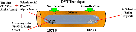 |
| | Fig. 1 The DVT technique for growing Sn1−βSbβSe single crystals is depicted schematically. | |
 |
| | Fig. 2 Photographs of as-grown Sn1−βSbβSe (β = 0, 0.05, 0.10, 0.15, 0.20) crystals. | |
2.2 Characterization techniques
The crystals obtained after growth are characterized by EDAX and XPS to know their purity and present elemental composition. The morphological, structural, optical, and vibrational characterizations of as-grown Sn1−βSbβSe crystals are investigated by SEM, XRD, HR-TEM, UV-visible Spectroscopy, Raman Spectroscopy, and Photoluminescence Spectroscopy.
2.3 Pulse photo-response and photo-stability
As an application part, photo detectivity of the grown crystals was carried out using the setup shown in Fig. 3. Firstly, crystals of specific dimensions were selected from the grown crystals, the average size of the crystals are 0.3 micrometer thin and cleaned using acetone to remove contamination from the surface. This crystal was then mounted on the PCB specially designed to measure the photoconductivity of the crystals. Thin copper wires were fixed on the periphery of the crystals and soldered to the PCB junctions. The whole setup was then installed into the Keithly-4200 semiconductor characterization system (SCS) for the analysis of the pulse photo response and photostability of pure and doped samples was studied under a monochromatic source of wavelength 670 nm and intensity of 30 mW cm−2 at zero biasing voltage firstly on day one and then the same samples preserved for 50 days and stability of photodetectors after 50 days was observed.
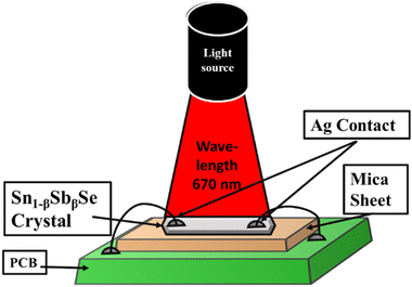 |
| | Fig. 3 Schematic representation of pulse photo response set-up. | |
3. Results and discussions
3.1 Chemical, structural and optical properties of the as grown Sn1−βSbβSe (β = 0, 0.05, 0.10, 0.15, 0.20) crystals
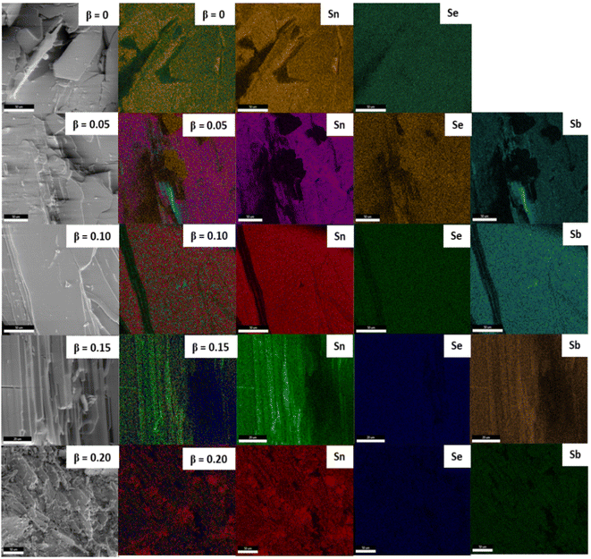
Firstly, to know the chemical composition and purity of the as-grown crystals of antimony doped tin selenium EDAX analysis was adopted. No foreign peaks were seen in the EDAX spectra of pure and doped samples as presented in Fig. 4. This confirms that the as-grown pure and doped samples grown under similar conditions are nearly stoichiometric in proportion. The elemental composition of both wt% taken and wt% obtained from EDAX is presented in the (ESI Table S2.†) The elemental mapping of, pure and doped samples are presented in Fig. 5, which maps the distribution of different constituent elements of the crystals.51,52
 |
| | Fig. 4 The EDAX Spectra of Sn1−βSbβSe (β = 0, 0.05, 0.10, 0.15, 0.20) crystals. | |
 |
| | Fig. 5 The EDAX mapping Spectra of Sn1−βSbβSe (β = 0, 0.05, 0.10, 0.15, 0.20) crystals. | |
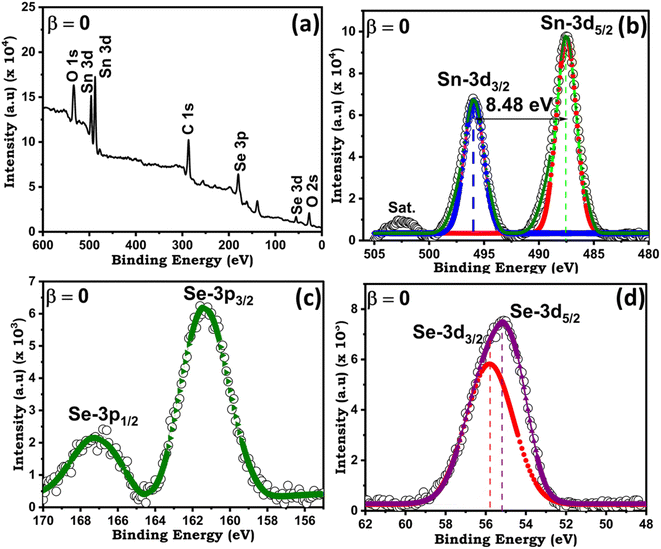
X-ray photoelectron spectroscopy was also carried out to confirm the elemental composition of the pure and doped samples. Fig. 6(a) presents the XPS scans of pure SnSe crystal, the spectra reveal the presence of Sn and Se along with the presence of oxygen. Fig. 6(a) depicts the XPS peaks of the Sn at the higher energy side, while the Se peaks are observed at the lower energy side. The Se peak is a singlet type of peak comprising the Se 3d3/2 and Se 3d5/2. The 3d3/2 and 3d5/2 are positioned at 487.49 and 495.92 eV with a peak difference of 8.48 eV for Sn whereas for Se it shows the reflections of 3d3/2, 3d5/2, 3p3/2 and 3p1/2 states at 55.16, 55.78, 161.36 and 167.15 eV respectively are shown in Fig. 6(b–d). The XPS scans of Sn1−βSbβSe (β = 0, 0.05, 0.10, 0.15, 0.20) presented in supplementary (ESI Fig. S2, S3, S4, and S5†) evincing the presence of 3d5/2, 3d3/2, 3p3/2, 3p1/2 states of Sn, Se, and Sb at different binding energies as shown in the Table 1. The results obtained from XPS analysis are matching with other published work.53–55
 |
| | Fig. 6 (a) The XPS full range spectra of SnSe crystal for (b) Se 3d3/2 & 3d5/2 (c) Se 3p3/2 & 3p5/2 and (d) Sn 3d5/2 & 3d3/2. | |
Table 1 The XPS parameters of the as grown compounds of Sn1−β SbβSe (β = 0, 0.05, 0.10, 0.15, 0.20)
| Compound |
β = 0 |
β = 0.05 |
β = 0.10 |
β = 0.15 |
β = 0.20 |
| Binding energy (eV) |
| Se 3d3/2 |
55.16 |
54.64 |
54.94 |
54.53 |
54.91 (eV) |
| Se 3d5/2 |
55.78 |
55.13 |
55.86 |
54.67 |
55.45 |
| Se 3p3/2 |
161.36 |
160.84 |
161.01 |
160.63 |
160.98 |
| Se 3p1/2 |
167.15 |
166.45 |
166.98 |
166.30 |
167.24 |
| Sn 3d5/2 |
487.49 |
486.72 |
487.43 |
486.53 |
487.06 |
| Sn 3d3/2 |
495.92 |
495.16 |
495.67 |
495.01 |
495.16 |
| Sb 3d5/2 |
— |
531.46 |
531.33 |
530.69 |
531.11 |
| Sb 3d3/2 |
— |
540.19 |
540.17 |
539.81 |
540.66 |
| Sb3+ |
— |
532.55 |
533.83 |
531.07 |
534.49 |
| O 1s |
531.32 |
533.91 |
534.30 |
531.30 |
534.61 |
Surface topographic properties were investigated by employing optical microscopy are shown in (ESI Fig. S6†) represents the flat layered growth of the crystals. Further, the investigation of the surface was studied by scanning electron microscope Philips FESEM -XL 30. Fig. 7(a) shows the presence of a flat surface due to uniform growth of layers whereas Fig. 7(b–d) depicts the layered growth at the boundary of the crystal and Fig. 7(e) presents randomly oriented elongated flakes.
 |
| | Fig. 7 The SEM image of (a–e) Sn1−βSbβSe (β = 0, 0.05, 0.10, 0.15, 0.20) crystals. | |
The structural analysis of the as-grown crystals and doped crystals was investigated by powder X-ray diffraction (Rigaku Ultima 4) using the Cu Kα radiation, in the 2θ range of 10° to 80°. Fig. 8(a) shows the XRD pattern of the pure and doped crystals of Sn1−βSbβSe (β = 0, 0.05, 0.10, 0.15, 0.20), reflecting the highest intensity and most prominent peak (400) be positioned roundabout, at 2θ = 31.07°. The enlarged image of the peak (400) depicted in Fig. 8(b) ascertains the shifting of the peak towards the higher angle side that corresponds to the substitution of Sb in the host SnSe structure upon doping. This shift in the peak position of the (400) plane upon doping can be attributed to the Vegard's law, which affirms the dopant can shift the peak position in the host material but alone it cannot produce an individual peak. The atomic radius of Sn (i.e. 225 pm) is greater than Sb (i.e. 206 pm), hence the shift in peak position also indicates and confirms the proper substitution of the Sb atom on the Sn atoms in the orthorhombic structure of SnSe belonging to Pnma(62) space group. The results obtained from XRD analysis match well with the JCPDS No. 01-078-979.56 The sharpness of the peak corroborates the enhanced crystallinity of the pure and doped crystals. The crystallite size (t), Micro-Strain (ε), and Dislocation Density (δ) of all the peaks were evaluated using the Debye Scherer expression from the given (supplementary equation No. 1 to 3).51,55,57 The other crystallographic parameters such as lattice constant a, b, c, strain, dislocation density, unit cell volume, and c/a ratio were also calculated from the XRD patterns and tabulated in (ESI Table S3.†) The crystallite size decreases on increasing the Sb content in the SnSe host material. This decrease in the crystallite size could be due to the atomic radius mismatch between Sb and Sn. Since Sb is having lower atomic radius as compared to Sn, hence this could lead to an increase in the strain and dislocation density values that can be ascertained from the magnitudes of strain and dislocation density as presented. (ESI Table S3†).
 |
| | Fig. 8 (a)The XRD image of Sn1−βSbβSe (β = 0, 0.05, 0.10, 0.15, 0.20) crystals. (b) Dominant peck shifting towards SnSe to Sb doped SnSe. | |
Fig. 9(a–e) shows the HRTEM images of pure and doped crystals of Sn1−βSbβSe (β = 0, 0.05, 0.10, 0.15, 0.20) ascribing the nano-flakes of grown samples and possess an interlayer spacing of 0.28 nm as shown in Fig. 9(f–j), which is in concurrence with the results obtained from XRD analysis for the (4 0 0) plane (JCPDS Card no. 01-078-9791).56,58–62 The spot patterns observed from the selected area electron diffraction ascribe the single crystalline nature of the pure and doped crystals of Sn1−βSbβSe as represented in Fig. 9(k–o). Diffraction planes observed from selected area electron diffraction are accord with the XRD diffraction planes.
 |
| | Fig. 9 (a–e) The HR-TEM image of Sn1−βSbβSe (β = 0, 0.05, 0.10, 0.15, 0.20) crystals. (f–j) The ringes of Sn1−βSbβSe (β = 0, 0.05, 0.10, 0.15, 0.20) crystals. (k–o) The SAED spot patterns of Sn1−βSbβSe (β = 0, 0.05, 0.10, 0.15, 0.20) crystals. | |
In order to study the vibrational properties of Sn1−βSbβSe (β = 0, 0.05, 0.10, 0.15, 0.20) crystals Raman spectroscopy (with excitation wavelength 532 nm laser) was utilized. Fig. 10(a) depicts the Raman Spectra of Sn1−βSbβSe (β = 0, 0.05, 0.10, 0.15, 0.20) evincing the B3g phonon mode at 108 cm−1 and Ag phonon mode at 118 cm−1. Both the phonon modes Ag and B3g arise due to the characteristics of planar vibration of SnSe.63 A clear red shift in the peak position with increasing concentration of Sb is observed in the Raman spectra of Sn1−βSbβSe shown in Fig. 10(b). This shifting in the peak could be assigned to the substitution of Sb on the Sn lattice sites due to variations in their atomic radius. The results obtained from XRD, HRTEM, and Raman analysis confirm the substitutional doping and it also matches well with other published reports.63,64
 |
| | Fig. 10 (a) The Raman image of Sn1−βSbβSe (β = 0, 0.05, 0.10, 0.15, 0.20) crystals. (b) The Raman shift towards sb incorporation of SnSe. | |
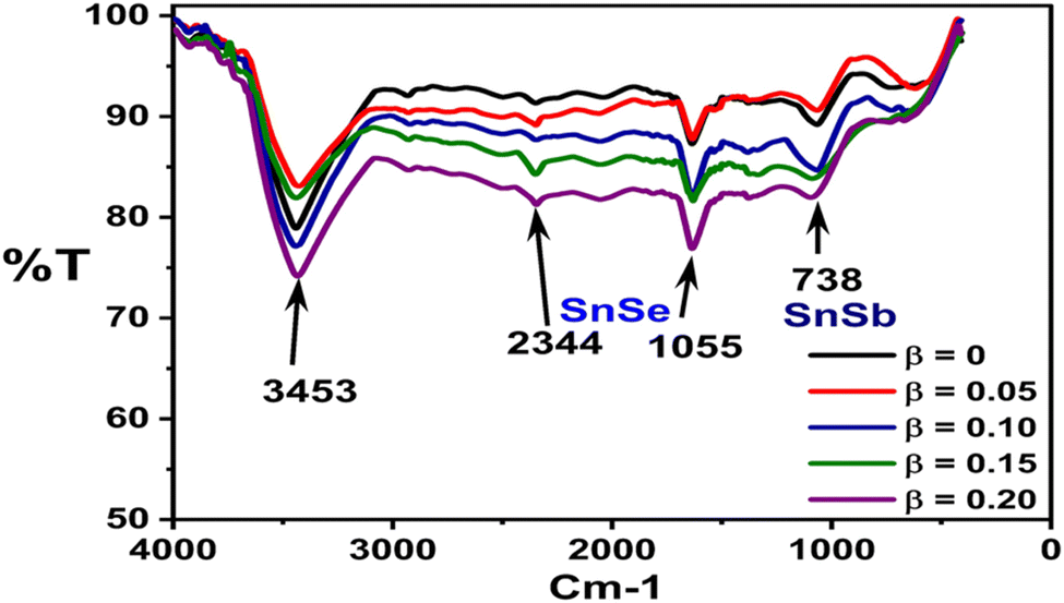
The FTIR spectra recorded in the wavenumber range of 4000 cm−1 to 0 cm−1 of the pure and doped crystals depicted in Fig. 11 reveal the presence of SnSe peaks at 2344cm−1 and 1055 cm−1. However, an additional peak at 738cm−1 attributes the phase formation of Sb with SnSe. The results obtained from FTIR analysis are in agreement with the other published reports in the literature.65–68
 |
| | Fig. 11 The FTIR image of Sn1−βSbβSe (β = 0, 0.05, 0.10, 0.15 and 0.20) crystals. | |
To study the optical parameters of the as-grown pristine and doped crystals, UV-visible spectroscopic analysis was carried out in the absorption mode, the wavelength range of 350 nm to 800 nm. The spectra presented in Fig. 12(a) show the absorption edge between 400 to 500 nm. Using Tauc plot equations (ESI eqn 4 to 6) of indirect allowed transition energy (αhν)1/2 versus photon energy (hν) the indirect energy band gap of pure and doped crystals is estimated by extrapolating the linear portion of the graph to the zero-absorption edge (i.e., α = 0) as presented in the Fig. 12(a) and (ESI Fig. S7(a–j)†) for SnSe and Sn1−βSbβSe (β = 0, 0.05, 0.10, 0.15, 0.20) crystals respectively. The indirect energy band gap of the pure and doped crystals is tabulated in Table no 2. Moreover, Fig. 12(b–f) and (ESI Fig. S6(a–j)†) evince a few discontinuities in the spectra of indirect energy bandgap occurring due to the interband transition taking place due to absorption and emission of phonons. This undulating nature in the spectra can be observed upon enlarging the portion of discontinuities seen in the (ESI Fig. S6(a–j)†). The method presented by Koshkin and Elkolashky69,70 equations presented in (ESI eqn 4 to 6) is employed to make certain specific measurements at the point of discontinuities. The other optical parameters such as Urbach energy and steepness parameter62,71 is presented in Table 2.
 |
| | Fig. 12 (a) UV-vis absorption spectroscopy and (b–f) indirect band-gap of Sn1−βSbβSe (β = 0, 0.05, 0.10, 0.15, 0.20) crystals. | |
Table 2 The UV VIS spectroscopy parameters of as grown Sn1−βSbβSe (β = 0, 0.05, 0.10, 0.15, 0.20) crystals
| Samples |
Eg (eV) |
E'g (eV) |
Ep1 (meV) |
Ep2 (meV) |
EU |
σ |
| β = 0 |
1.18 |
1.5724 |
8.25 |
7.65 |
2.116805 |
0.012213 |
| β = 0.05 |
1.24 |
1.5714 |
7.55 |
4.55 |
1.744014 |
0.014823 |
| β = 0.10 |
1.37 |
1.5754 |
10.71 |
3.35 |
2.090782 |
0.012365 |
| β = 0.15 |
1.40 |
1.5687 |
11.11 |
3.21 |
2.036328 |
0.012695 |
| β = 0.20 |
1.46 |
1.5887 |
24.81 |
7.75 |
1.10715 |
0.02335 |
Fig. 13 presents the PL spectra of pure and doped samples of Sn1−βSbβSe (β = 0, 0.05, 0.10, 0.15, 0.20) crystals. A strong peak in the wavelength range of 400 to 500 nm can be clearly seen. The result obtained are matching well with the previously published reports in the literature55,72 and the obtained results are also corroboration with the results of UV-visible spectroscopy.
 |
| | Fig. 13 The Photoluminescence spectroscopy of Sn1−βSbβSe (β = 0, 0.05, 0.10, 0.15, 0.20) crystals. | |
3.2 Self-biased pulse photo response and durability of the Sn1−βSbβSe (β = 0, 0.05, 0.10, 0.15, 0.20) photodetectors
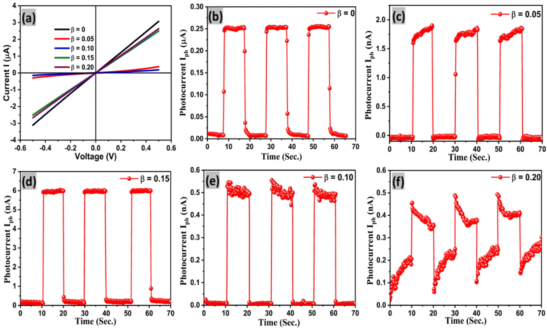
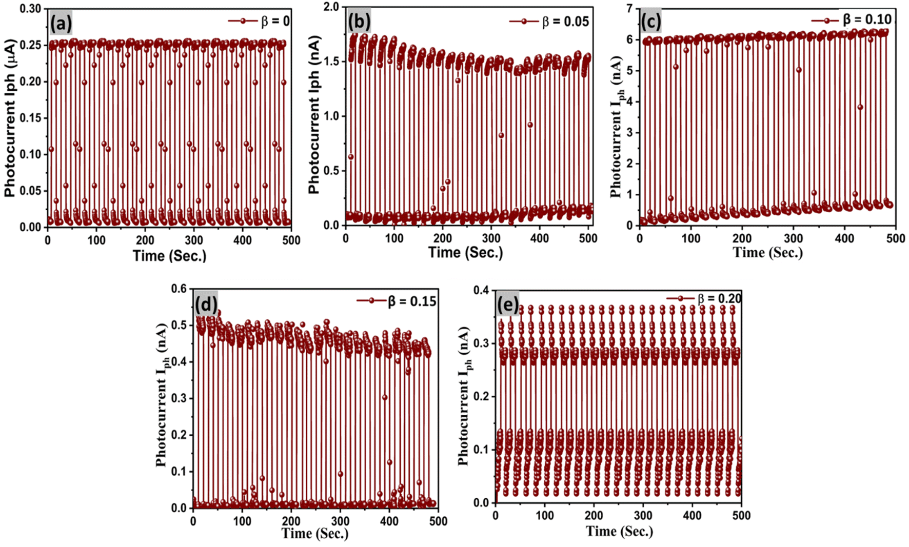
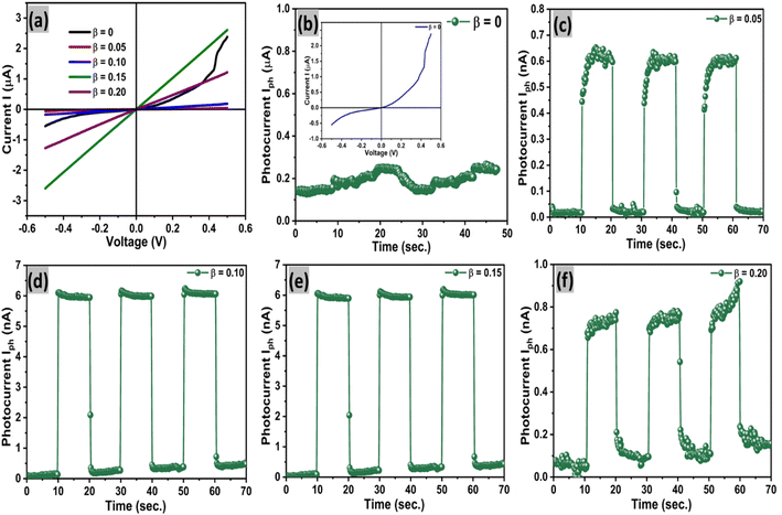
The pulse photo conduction properties of Sn1−βSbβSe (β = 0, 0.05, 0.10, 0.15, 0.20) crystal are explored due to its intensive applications in optoelectronics. Time resolved pulse photo conduction properties of pure and doped crystals at zero biasing voltage are recorded in the present investigation using Keithley 4200 SMU and a monochromatic source (light source having wavelength 670 nm and intensity 30mWcm−2) under ON and OFF conditions. A detailed description and method of the fabrication of the photo-detector are discussed in the experimental section. Fig. 14(a) presents linear I–V characteristics of the prepared Sn1−βSbβSe (β = 0, 0.05, 0.10, 0.15, 0.20) photo-detector, inferring the good ohmic contacts between the crystal surface and the copper electrode. The time resolved pulse photo response of pure and doped crystals of Sn1−βSbβSe (β = 0, 0.05, 0.10, 0.15, 0.20) are presented in Fig. 14(b–f) and 15(a–e) clearly evinces stable and repeating pulse photo response. It can be inferred from the Fig. 14(b) that on switching ON the light source a sudden increase in photo-current (i.e. 0.25 μA) for pure SnSe can be observed. This increase in photocurrent is due to the generation of electron hole pairs upon switching the light source. A similar trend is observed for all other doped samples shown in Fig. 14(c–f). The device response time, responsivity, and detectivity are important parameters for deciding the potentiality of the material as a photodetector. Quick rise time (τr = 0.46 s) and slow decay time (τd = 0.66 s) of the photocurrent can also be observed from the repeating pulse response. The slow decay time here ascribes to, the trapping of photo-generated charge carriers for a longer period of time within the deep level defect states arising within the energy band gap due to the high-temperature growth of the samples.62 In addition, due to mechanical exfoliation and absorption of oxygen by the surface, the slow decay in photocurrent could also be observed [40]. Responsivity, detectivity, and sensitivity of the prepared detector were evaluated using the expressions mentioned in the ESI (eqn. 12 to 15) and presented in Table 3.
 |
| | Fig. 14 (a) The I–V characteristics of Sn1−βSbβSe (β = 0, 0.05, 0.10, 0.15, 0.20) crystal photodetectors (b–f). The pulse photo response of Sn1−βSbβSe (β = 0, 0.05, 0.10, 0.15, 0.20) crystal photodetectors on first day. | |
 |
| | Fig. 15 (a–e) The stable pulse photo response of Sn1−βSbβSe (β = 0, 0.05, 0.10, 0.15, 0.20) crystal photodetectors for 500 s. | |
Table 3 The detectors parameters of Sn1−βSbβSe (β = 0, 0.05, 0.10, 0.15, 0.20) photodetectors on first day
| Sample |
Photocurrent (Iph) |
Sensitivity (S) |
Responsivity (Rλ) |
Detectivity (D) Jones |
Rise time (sec.) |
Decay time (sec.) |
| β = 0 |
2.48 × 10⁻⁷ |
3.18 × 101 |
3.68 × 10⁻⁴ |
1.10 × 10⁹ |
0.46 |
0.62 |
| β = 0.05 |
1.91 × 10⁻⁹ |
6.18 × 10² |
2.84 × 10⁻⁶ |
4.27 × 10⁸ |
0.16 |
0.33 |
| β = 0.10 |
5.41 × 10⁻¹⁰ |
8.86 × 101 |
8.01 × 10⁻⁷ |
8.60 × 10⁷ |
0.19 |
0.28 |
| β = 0.15 |
6.01 × 10⁻⁹ |
9.50 × 101 |
8.91 × 10⁻⁶ |
2.97 × 10⁸ |
0.14 |
0.16 |
| β = 0.20 |
4.39 × 10⁻¹⁰ |
2.37 × 101 |
6.50 × 10⁻⁷ |
4.01 × 10⁷ |
0.21 |
0.23 |
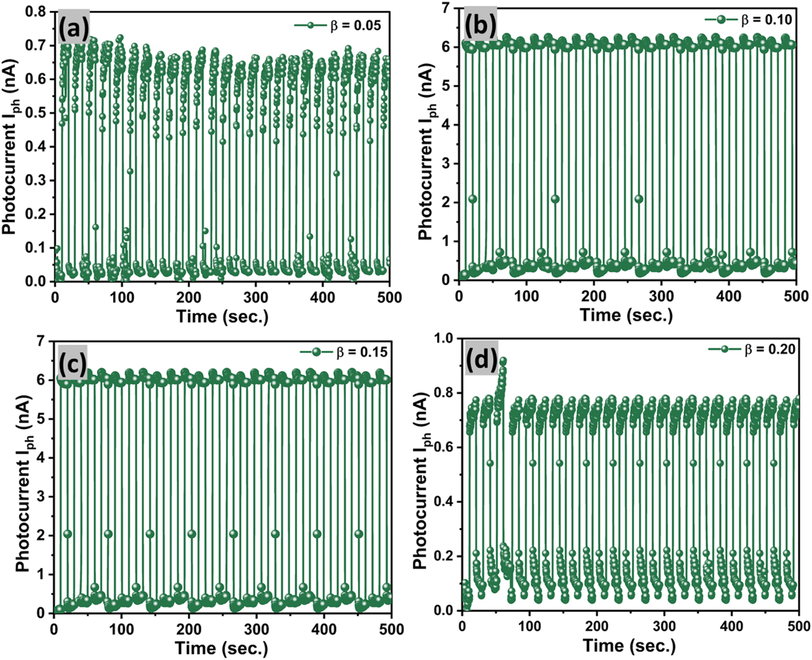
The pulse response of the prepared detector left in an open atmosphere for 50 days was also recorded to investigate the stability of the device. Firstly, the I–V characteristics of the detectors were measured as shown in Fig. 16(a). I–V characteristics of SnSe show Schottky nature, while doped photodetectors depict ohmic I–V characteristics in similar conditions. Fig. 16(b–f) and 17(a–d) present the pulse photo response of pure and doped samples. It can be inferred from the figures that the pulse response and switching actions of doped samples obtained after 50 days are stable and they give similar results as they were given on day 1. While SnSe sample is not behaving as a photodetector because it may have an oxide layer on the surface and that's why it gives Schottky behavior as shown in Fig. 16(a) and b. The photodetection parameters of the all samples after 50 days are presented in Table 4 and this parameters are similarly to the first day. The rise time and decay time are same for all the devices and after 1st day and 50 days there are some changes in some devices and all the devices have durability and stability which is a good indication and they can be used for future commercial and industrial life. The results compared with the reported article shows in Table 5 points that the Sn1−βSbβSe photodetectors present tremendous photo-detectivity under self-biased condition. Moreover, rise time and decay time are also very tiny for the Sn1−βSbβSe photodetectors. Here we can affirm from the obtained results that our photo detecting parameter (i.e., rise and decay time) is much better than the other materials.59,60,73,74
 |
| | Fig. 16 (a) I–V characteristics of Sn1−βSbβSe (β = 0, 0.05, 0.10, 0.15, 0.20) crystals photodetectors (b–f) pulse photo response of Sn1−βSbβSe (β = 0, 0.05, 0.10, 0.15, 0.20) crystal photodetectors after 50 days. | |
 |
| | Fig. 17 (a–d) Stable pulse photo response of Sn1−βSbβSe (β = 0, 0.05, 0.10, 0.15, 0.20) crystal photodetectors for 500 s. | |
Table 4 The detectors parameters of Sn1−βSbβSe (β = 0, 0.05, 0.10, 0.15, 0.20) photodetectors after 50 days
| Sample |
Photocurrent (Iph) |
Sensitivity (S) |
Responsivity (Rλ) |
Detectivity (D) Jones |
Rise time (sec) |
Decay Time (sec) |
| β = 0 |
— |
— |
— |
— |
— |
— |
| β = 0.05 |
6.45 × 10⁻¹⁰ |
4.31 × 101 |
9.55 × 10⁻⁷ |
6.55 × 10⁷ |
0.18 |
0.14 |
| β = 0.10 |
6.15 × 10⁻⁹ |
4.11 × 10² |
9.10 × 10⁻⁶ |
6.24 × 10⁸ |
0.16 |
0.33 |
| β = 0.15 |
6.04 × 10⁻⁹ |
4.04 × 10² |
8.95 × 10⁻⁶ |
6.14 × 10⁸ |
0.15 |
0.31 |
| β = 0.20 |
7.59 × 10⁻¹⁰ |
5.08 × 101 |
1.12 × 10⁻⁶ |
7.71 × 10⁷ |
0.16 |
0.16 |
Table 5 The photodetection parameters of Sn1−βSbβSe crystals compared to previously reported TMC and TMDC materials
| Samples/bias voltage |
Photocurrent (μA) |
Responsivity (mA W−1) |
Detectivity (Jones) |
EQE (%) |
Rise time (sec) |
Decay time (sec) |
Ref |
| SnSe Crystal/0 V |
0.24 |
0.368 |
1.10 × 10⁹ |
— |
0.46 |
0.62 |
Present Wwork |
| Sn0.85 Sb0.15 Se/0 V |
0.006 |
8.91 × 10⁻⁶ |
2.97 × 10⁸ |
— |
0.14 |
0.16 |
|
| Ni0.2Sn0.8Se crystal/0.6 V |
0.053 |
0.402 |
2.91 × 10⁹ |
— |
0.41 |
1.44 |
78 |
| Cu0.2Sn0.8Se nanoparticles/1.5 V |
0.32 |
8.55 |
2.00 × 10⁹ |
1.59 |
1.90 |
1.90 |
79 |
| Cu0.4Sn0.6Se nanoparticles/1.5 V |
0.67 |
13.55 |
1.98 × 10¹⁰ |
2.50 |
1.3 |
2.0 |
80 |
| Sb0.1Sn0.9Se2 crystal/0.6 V |
1.88 |
43.45 |
18.25 × 10¹¹ |
47.28 |
4.40 |
4.50 |
61 |
| Sb0.2Sn0.8Se2 crystals/0.6 V |
1.05 |
24.28 |
10.95 × 10¹¹ |
39.31 |
4.60 |
4.60 |
61 |
| Sb0.3Sn0.7Se2 crystals/0.6 V |
0.48 |
11.12 |
5.54 × 10¹¹ |
34.11 |
4.60 |
4.70 |
61 |
| V0.75W0.75Se2 crystals/0.3 V |
11.38 |
253.00 |
2.03 × 10⁹ |
46.91 |
1.80 |
2.90 |
81 |
| V0.15Sn0.85Se2 crystals/1 mV |
1.26 |
33.30 |
12.5 × 10⁹ |
6.17 |
1.90 |
2.00 |
82 |
| V0.25Sn0.75Se2 crystals/1 mV |
1.32 |
35.08 |
7.58 × 10⁹ |
6.50 |
0.90 |
0.90 |
82 |
| V0.5Sn0.5Se2 crystals/1 mV |
4.39 |
106.95 |
7.32 × 10⁹ |
19.82 |
0.60 |
1.30 |
82 |
| Sb0.1Mo0.9Se2 crystals/5 V |
— |
163.32 |
8.47 × 10⁷ |
28.62 |
— |
— |
83 |
| Sb0.5Mo0.5Se2 crystals/3 V |
11.48 |
1435.00 |
0.29 × 10⁷ |
— |
0.97 |
1.00 |
84 |
Photodetectors exhibit stable photocurrent after 50 days. It indicated that the device possesses longer durability and have a lifetime of more than 50 days. These outstanding performances could be potentially applicable for practical applications. The results revel admirable stability and ecological durability of the photodetectors based on the Sn1−βSbβSe (β = 0, 0.05, 0.10, 0.15, 0.20) single crystals, which is necessary for the relatively inexpensive, portable and mechanical stable optoelectronic applications. Finally, this work also validates an efficacious methodology for developing imperially stable and prolong durable large area photodetectors.75–77
4. Conclusions
In the present investigation Sn1−βSbβSe where (β = 0, 0.05, 0.10, 0.15, and 0.20) single crystals were grown using the direct vapor transport technique in a dual zone horizontal furnace. The elemental compositions of the grown samples were confirmed by EDAX and XPS which affirms the presence of Sb, Sn, and Se elements. The surface morphological properties were studied by SEM, confirming the layer-by-layer growth of Sn1−βSbβSe (β = 0, 0.05, 0.10, 0.15, 0.20) crystals. The structural properties were studied by XRD reflecting the highest intensity peak (400) located at 2θ = 31.07°. XRD analysis also confirms the orthorhombic structure of the samples. The HRTEM and Electron diffraction study ascertains the orthorhombic structure of the samples. The vibrational properties of the Sn1−βSbβSe (β = 0, 0.05, 0.10, 0.15, 0.20) crystals confirm the presence of B2g and Ag modes of vibrations. The results obtained from XRD, HRTEM, and Raman spectroscopy affirm the substitutional doping of Sb on Sn lattice sites. The optical properties of the samples were studied by UV-visible and Photoluminescence Spectroscopy. The indirect energy band gap obtained from the Tauc plot of pure and doped samples varies from 1.18 eV to 1.46 eV. The PL intensity peak obtained at 400 to 500 nm confirms the energy band suitable for optoelectronic device applications. The pulse photo response recorded at 0 V biasing shows a quick response and slow decay of photocurrent. This slow decay of photocurrent is ascribed to the presence of defect states that traps the photo-generated charge carriers. Photodetection results depict the improvement in the stability and durability of Antimony doped SnSe photodetectors compared to pristine SnSe photodetectors.
Data availability
Data are available on request due to privacy or other restrictions.
Author contributions
Hirenkumar Shantilal Jagani: conceptualization, writing – original draft, formal Analysis, investigation, methodology. Vijay Dixit: writing – review & editing, validation, visualization, conceptualization. Abhishek Patel: writing – review & editing, validation, visualization, formal Analysis. Jagrutiba Gohil: data curation, formal Analysis. Vivek M. Pathak: project administration, resources, conceptualization, supervision, validation.
Conflicts of interest
There are no conflicts of interest to declare.
Acknowledgements
The authors H. S. Jagani and others are thankful to the Government of Gujarat for providing financial assistance under the SHODH scheme (Student Ref No: 201901640036). The authors H. S. Jagani highly acknowledge Prof. K. D. Patel and Prof. G. K. Solanki, Department of Physics, Sardar Patel University, Gujarat, India for useful discussion about device physics of Pulse photodetector for device parameters investigation for the present article. I am thankful to Prof. P. K. Jha and Mr Sharadbhai, Department of Physics, The Maharaja Sayajirao University of Baroda, Vadodara, for providing the Raman spectroscopy. I am thankful to Prof. K.V.R. Murthy, Department of Physics, The Maharaja Sayajirao University of Baroda, for providing the Photoluminescence Spectroscopy. The author would also like to thank UGC-DAE-Consortium for Scientific Research, Indore for providing the characterization facilities of X-ray Photoelectron Spectroscopy (XPS). The author would also like to thank Dr. Uday Deshpande, UGC-DAE-Consortium for Scientific Research, Indore for the XPS analysis.
References
- J. Yan, S. Deng, D. Zhu, H. Bai and H. Zhu, Nano Energy, 2022, 97, 107188 CrossRef.
- Y. Yu, T. Xiong, Z. Guo, S. Hou, J. Yang, Y. Y. Liu, H. Gu and Z. Wei, Fundam. Res., 2022, 2667–3258 Search PubMed.
- S. Nair, J. Joy, K. D. Patel, P. Pataniya, G. K. Solanki, V. M. Pathak and C. K. Sumesh, in AIP Conference Proceedings, American Institute of Physics Inc., 2018, vol. 1961 Search PubMed.
- O. logo, C. L. O. logo, Y. L. Tianying He and a C. Lan, ORCID logo a Sihan Zhou,a Yongjun Li,a Yi Yin, J. Mater. Chem. C, 2021, 9, 3846–3853 RSC.
- M. Yalcin and F. Yakuphanoglu, Optik (Stuttg), 2019, 183, 1099–1105 CrossRef CAS.
- D. E. Yildiz, Ş. Altindal and H. Kanbur, J. Appl. Phys., 2008, 103(12) DOI:10.1063/1.2936963.
- D. Kishore Kumar, J. Loskot, J. Kříž, N. Bennett, H. M. Upadhyaya, V. Sadhu, C. Venkata Reddy and K. R. Reddy, Sol. Energy, 2020, 199, 570–574 CrossRef CAS.
- K. Patel, T. Parangi, G. K. Solanki, M. K. Mishra, K. D. Patel and V. M. Pathak, Eur. Phys. J. Plus, 2021, 136, 743 CrossRef CAS.
- A. Hirohata, K. Yamada, Y. Nakatani, L. Prejbeanu, B. Diény, P. Pirro and B. Hillebrands, J. Magn. Magn. Mater., 2020, 509 Search PubMed.
- M. A. Dar, D. Govindarajaran, K. M. Batoo, M. Hadi and G. N. Dar, Mater. Technol., 2021, 37(10), 1396–1409 CrossRef.
- L. Hao, Z. Wang, H. Xu, K. Yan, S. Dong, H. Liu, Y. Du, Y. Wu, Y. Liu and M. Dong, 2d Mater, 2019, 6 DOI:10.1088/2053-1583/ab15f7.
- P. Chauhan, A. B. Patel, G. K. Solanki, H. K. Machhi, S. S. Soni, V. M. Pathak, V. Patel, S. Narayan and P. K. Jha, Adv. Opt. Mater., 2021, 9 DOI:10.1002/adom.202100993.
- V. P. Jethwa, K. Patel, N. Som, V. M. Pathak, K. D. Patel, G. K. Solanki and P. K. Jha, Appl. Surf. Sci., 2020, 531 DOI:10.1016/j.apsusc.2020.147406.
- Y. Zhong, L. Zhang, V. Linseis, B. Qin, W. Chen, L. D. Zhao and H. Zhu, Nano Energy, 2020, 72 DOI:10.1016/j.nanoen.2020.104742.
- L. Hao, Z. Wang, H. Xu, K. Yan, S. Dong, H. Liu, Y. Du, Y. Wu, Y. Liu and M. Dong, 2d Mater, 2019, 6 DOI:10.1088/2053-1583/ab15f7.
- H. Patel, K. Patel, A. Patel, H. Jagani, K. D. Patel, G. K. Solanki and V. M. Pathak, J. Electron. Mater., 2021, 50, 5217–5225 CrossRef CAS.
- S. U. Gupta, A. G. Dalvaniya, C. Limberkar, K. D. Patel, G. K. Solanki, V. M. Pathak, P. M. Pataniya, C. K. Sumesh, N. N. Som, P. K. Jha and V. Patel, J. Non-Cryst. Solids, 2022, 578, 121353 CrossRef CAS.
- Y. X. Chen, Z. H. Ge, M. Yin, D. Feng, X. Q. Huang, W. Zhao and J. He, Adv. Funct. Mater., 2016, 26, 6836–6845 CrossRef CAS.
- Y. Huang, L. Li, Y. H. Lin and C. W. Nan, J. Phys. Chem. C, 2017, 121, 17530–17537 CrossRef CAS.
- E. P. Mukhokosi, S. B. Krupanidhi and K. K. Nanda, Sci. Rep., 2017, 7 DOI:10.1038/s41598-017-15519-x.
- K. Patel, G. Solanki, K. Patel, V. Pathak and P. Chauhan, Eur. Phys. J. B, 2019, 92 DOI:10.1140/epjb/e2019-100306-8.
- J. Yao and G. Yang, Adv. Sci., 2022, 9, 2103036 CrossRef.
- Z. Cheng, R. Cao, K. Wei, Y. Yao, X. Liu, J. Kang, J. Dong, Z. Shi, H. Zhang and X. Zhang, Adv. Sci., 2021, 8, 2003834 CrossRef PubMed.
- C. Limberkar, A. Patel, K. Patel, S. Nair, J. Joy, K. D. Patel, G. K. Solanki and V. M. Pathak, J. Alloys Compd., 2020, 846 DOI:10.1016/j.jallcom.2020.156391.
- K. Patel, G. K. Solanki, K. D. Patel, V. M. Pathak, P. Chauhan and A. Patel, J. Nano- Electron. Phys., 2020, 12 DOI:10.21272/JNEP.12(2).02005.
- C. L. Chen, H. Wang, Y. Y. Chen, T. Day and G. J. Snyder, J. Mater. Chem. A, 2014, 2, 11171–11176 RSC.
- L. Zhang, J. Wang, Q. Sun, P. Qin, Z. Cheng, Z. Ge, Z. Li and S. Dou, Adv. Energy Mater., 2017, 7 DOI:10.1002/aenm.201700573.
- E. K. Chere, Q. Zhang, K. Dahal, F. Cao, J. Mao and Z. Ren, J. Mater. Chem. A, 2016, 4, 1848–1854 RSC.
- T. R. Wei, C. F. Wu, X. Zhang, Q. Tan, L. Sun, Y. Pan and J. F. Li, Phys. Chem. Chem. Phys., 2015, 17, 30102–30109 RSC.
- J. H. Kim, S. Oh, Y. M. Kim, H. S. So, H. Lee, J. S. Rhyee, S. D. Park and S. J. Kim, J. Alloys Compd., 2016, 682, 785–790 CrossRef CAS.
- J. Gao, H. Zhu, T. Mao, L. Zhang, J. Di and G. Xu, Mater. Res. Bull., 2017, 93, 366–372 CrossRef CAS.
- X. Shi, A. Wu, T. Feng, K. Zheng, W. Liu, Q. Sun, M. Hong, S. T. Pantelides, Z. G. Chen and J. Zou, Adv. Energy Mater., 2019, 9 DOI:10.1002/aenm.201803242.
- U. M. E. D. A. Jun-ichi, J. Phys. Soc. Japan, 1961, 124 Search PubMed.
- C. Yamamoto, X. He, T. Katase, K. Ide, Y. Goto, Y. Mizuguchi, A. Samizo, M. Minohara, S. Ueda, H. Hiramatsu, H. Hosono and T. Kamiya, Adv. Funct. Mater., 2021, 31 DOI:10.1002/adfm.202008092.
- X. L. Shi, K. Zheng, W. di Liu, Y. Wang, Y. Z. Yang, Z. G. Chen and J. Zou, Adv. Energy Mater., 2018, 8 DOI:10.1002/aenm.201800775.
- N. K. Singh, S. Bathula, B. Gahtori, K. Tyagi, D. Haranath and A. Dhar, J. Alloys Compd., 2016, 668, 152–158 CrossRef.
- R. Chen, S. Li, J. Liu, Y. Li, F. Ma, J. Liang, X. Chen, Z. Miao, J. Han, T. Wang and Q. Li, Electrochim. Acta, 2018, 282, 973–980 CrossRef.
- C. Chang, Q. Tan, Y. Pei, Y. Xiao, X. Zhang, Y. X. Chen, L. Zheng, S. Gong, J. F. Li, J. He and L. D. Zhao, RSC Adv., 2016, 6, 98216–98220 RSC.
- F. Li, W. Wang, X. Qiu, Z. Zheng, P. Fan, J. Luo and B. Li, Inorg. Chem. Front., 2017, 4, 1721–1729 RSC.
- A. T. Duong, V. Q. Nguyen, G. Duvjir, V. T. Duong, S. Kwon, J. Y. Song, J. K. Lee, J. E. Lee, S. Park, T. Min, J. Lee, J. Kim and S. Cho, Nat. Commun., 2016, 7 DOI:10.1038/ncomms13713.
- T. R. Wei, G. Tan, X. Zhang, C. F. Wu, J. F. Li, V. P. Dravid, G. J. Snyder and M. G. Kanatzidis, J. Am. Chem. Soc., 2016, 138, 8875–8882 CrossRef CAS PubMed.
- M. Gharsallah, F. Serrano-Sánchez, N. M. Nemes, F. J. Mompeán, J. L. Martínez, M. T. Fernández-Díaz, F. Elhalouani and J. A. Alonso, Sci. Rep., 2016, 6 DOI:10.1038/srep26774.
- M. Hong, Z. G. Chen, L. Yang, T. C. Chasapis, S. D. Kang, Y. Zou, G. J. Auchterlonie, M. G. Kanatzidis, G. J. Snyder and J. Zou, J. Mater. Chem. A, 2017, 5, 10713–10721 RSC.
- J. C. Li, D. Li, X. Y. Qin and J. Zhang, Scr. Mater., 2017, 126, 6–10 CrossRef CAS.
- V. Kucek, T. Plechacek, P. Janicek, P. Ruleova, L. Benes, J. Navratil and C. Drasar, J. Electron. Mater., 2016, 45, 2943–2949 CrossRef CAS.
- M. A. Sattar, M. Benkraouda and N. Amrane, Physica B Condens. Matter., 2022, 633, 413789 CrossRef CAS.
- S. S. Ismailov, J. I. Huseynov, M. A. Musaev, I. I. Abbasov and V. A. Abdurakhmanova, Low Temp. Phys., 2020, 46, 1114–1120 CrossRef.
- D. I. Huseynov, M. I. Murguzov and S. S. Ismailov, Inorg. Mater., 2008, 44, 467–469 CrossRef.
- J. I. Huseynov and T. A. Jafarov, Semiconductors, 2012, 46, 430–432 CrossRef.
- V. Dixit, P. Chauhan, A. B. Patel, S. Narayan, P. K. Jha, G. K. Solanki, K. D. Patel and V. M. Pathak, Mater. Lett., 2019, 2 DOI:10.1016/j.mlblux.2019.100013.
- H. S. Jagani, S. U. Gupta, K. Bhoraniya, M. Navapariya, V. M. Pathak, G. K. Solanki and H. Patel, Adv. Mater., 2022, 3, 2425–2433 RSC.
- H. S. Jagani, A. Patel, J. Gohil and V. M. Pathak, Opt. Mater., 2022, 132, 112756 CrossRef.
- J. Dona, J. Archana, S. Kamalakannan, M. Prakash, K. Hara, S. Harish and M. Navaneethan, J. Alloys Compd., 2022, 899, 163269 CrossRef.
- X. L. Shi, K. Zheng, W. di Liu, Y. Wang, Y. Z. Yang, Z. G. Chen and J. Zou, Adv. Energy Mater., 2018, 8 DOI:10.1002/aenm.201800775.
- K. Patel, P. Chauhan, A. B. Patel, G. K. Solanki, K. D. Patel and V. M. Pathak, ACS Appl. Nano Mater., 2020, 3, 11143–11151 CrossRef CAS.
- JCPDS Card No. 01-078-9791.
- V. Dixit, S. Nair, J. Joy, C. U. Vyas, S. Narayan, P. K. Jha, G. K. Solanki and V. M. Pathak, J. Mater. Sci.: Mater. Electron., 2021, 32, 28739–28749 CrossRef CAS.
- G. Su, V. G. Hadjiev, P. E. Loya, J. Zhang, S. Lei, S. Maharjan, P. Dong, P. M. Ajayan, J. Lou and H. Peng, Nano Lett., 2015, 15, 506–513 CrossRef CAS PubMed.
- C. U. Vyas, P. Pataniya, C. K. Zankat, V. M. Pathak, K. D. Patel and G. K. Solanki, Mater. Sci. Semicond. Process., 2017, 71, 226–231 CrossRef CAS.
- J. Cao, Z. Wang, X. Zhan, Q. Wang, M. Safdar, Y. Wang and J. He, Nanotechnology, 2014, 25 DOI:10.1088/0957-4484/25/10/105705.
- M. Tannarana, P. Pataniya, G. K. Solanki, S. Babu Pillai, K. D. Patel, P. K. Jha and V. M. Pathak, Appl. Surf. Sci., 2018, 462, 856–861 CrossRef CAS.
- A. B. Patel, H. K. Machhi, P. Chauhan, S. Narayan, V. Dixit, S. S. Soni, P. K. Jha, G. K. Solanki, K. D. Patel and V. M. Pathak, ACS Appl. Mater. Interfaces, 2019, 11, 4093–4102 CrossRef CAS PubMed.
- L. Qiu, X. Lai and J. Jian, Mater. Charact., 2021, 172 DOI:10.1016/j.matchar.2020.110864.
- J. Guo, J. Jian, J. Liu, B. Cao, R. Lei, Z. Zhang, B. Song and H. Zhao, Nano Energy, 2017, 38, 569–575 CrossRef CAS.
- Y. Li, W. Zhang, H. Cai, J. Wang, X. Ren and P. Zhang, RSC Adv., 2015, 5, 105643–105650 RSC.
- H. Shi, A. Zhang, X. Zhang, H. Yin, S. Wang, Y. Tang, Y. Zhou and P. Wu, Nanoscale, 2018, 10, 4962–4968 RSC.
- S. Menon and M. Sarkar, in Materials Today: Proceedings, Elsevier Ltd, 2020, vol. 47, pp. 677–681 Search PubMed.
- B. Pejjai, V. R. Minnam Reddy, K. Seku, M. R. Pallavolu and C. Park, New J. Chem., 2018, 42, 4843–4853 RSC.
- V. M. Koshkin, V. R. Karas and L. P. Gal’chinetskii, Sov. Phys. Semicond., 1970, 3, 1186 Search PubMed.
- A. M. Elkorashy, J. Phys. Chem.
Solids, 1986, 47(5), 497–500 CrossRef.
- V. Dixit, S. Nair, J. Joy, C. U. Vyas, G. K. Solanki, K. D. Patel and V. M. Pathak, Mater. Sci. Semicond. Process., 2018, 88, 1–9 CrossRef.
- L. Das, A. Guleria and S. Adhikari, RSC Adv., 2015, 5, 61390–61397 RSC.
- S. U. Gupta, A. G. Dalvaniya, N. F. Patel, S. A. Bhakhar, S. Nair, J. Joy, K. D. Patel, G. K. Solanki, V. M. Pathak, N. N. Som, P. K. Jha and D. K. Panda, ACS Appl. Electron Mater., 2021, 3, 4859–4869 CrossRef.
- S. U. Gupta, A. G. Dalvaniya, C. Limberkar, K. D. Patel, G. K. Solanki, V. M. Pathak, P. M. Pataniya, C. K. Sumesh, N. N. Som, P. K. Jha and V. Patel, J. Non-Cryst. Solids, 2022, 578, 121353 CrossRef.
- G. Chen, W. Wang, C. Wang, T. Ding and Q. Yang, Adv. Sci., 2015, 2, 1500109 CrossRef PubMed.
- F. Guo, X. Li, B. Zhang, L. Zhang, H. Bai, Z. Zhang, Q. Yang, Y. Tan, X. Liu, Y. Song and Y. Huang, J. Mater. Sci.: Mater. Electron., 2019, 30, 19437–19443 CrossRef.
- J. Zheng, C. Luo, B. Shabbir, C. Wang, W. Mao, Y. Zhang, Y. Huang, Y. Dong, J. J. Jasieniak, C. Pan and Q. Bao, Nanoscale, 2019, 11, 8020–8026 RSC.
- J. Gohil, V. Jethwa, V. M. Pathak, G. K. Solanki, P. Chauhan, A. B. Patel, C. Zankat and N. Patel, J. Mater. Sci.: Mater. Electron., 2022, 33, 10086–10095 CrossRef CAS.
- K. Patel, G. K. Solanki, K. D. Patel, V. M. Pathak, P. Chauhan and A. Patel, J. Nano- Electron. Phys., 2020, 12, 02005 CAS.
- K. Patel, A. Patel, V. P. Jethwa, G. K. Solanki, K. D. Patel and V. M. Pathak, J. Mater. Sci.: Mater. Electron., 2022, 33, 8361–8367 CrossRef CAS.
- P. Pataniya, G. K. Solanki, K. D. Patel, V. M. Pathak and C. K. Sumesh, Mater. Res. Express, 2017, 4, 106306 CrossRef.
- C. K. Zankat, P. Pataniya, G. K. Solanki, K. D. Patel and V. M. Pathak, Mater. Lett., 2018, 221, 35–37 CrossRef CAS.
- V. Dixit, S. Nair, J. Joy, C. U. Vyas, G. K. Solanki, K. D. Patel and V. M. Pathak, Mater. Sci. Semicond. Process., 2018, 88, 1–9 CrossRef CAS.
- V. Dixit, P. Chauhan, A. B. Patel, S. Narayan, P. K. Jha, G. K. Solanki, K. D. Patel and V. M. Pathak, Mater. Lett., 2019, 2, 100013 CAS.
Footnote |
| † Electronic supplementary information (ESI) available: Table. S1. The growth parameters fixed for crystal growth of Sn1−βSbβSe (β = 0, 0.05, 0.10, 0.15, 0.20). Table. S2. Atomic percentage data obtain from EDAX spectra of as grown Sn1−β SbβSe (β = 0, 0.05, 0.10, 0.15, 0.20) crystals. Fig. S1. The XPS Spectra of Sb0.05Sn0.95Se crystal. Fig. S2. The XPS Spectra of Sb0.1Sn0.90Se crystal. Fig. S3.† The XPS Spectra of Sb0.15Sn0.85Se crystal. Fig. S4. The XPS Spectra of Sb0.2Sn0.8Se crystal. Table. S3. The XRD parameters of Sn1−βSbβSe (β = 0, 0.05, 0.10, 0.15, 0.20) crystals. Fig. S5. The optical microscopic images of Sn1−βSbβSe (β = 0, 0.05, 0.10, 0.15, 0.20) crystals. Fig. S6.† The energy stack and urbach energy of Sn1−βSbβSe (β = 0, 0.05, 0.10, 0.15, 0.20) crystals. See https://doi.org/10.1039/d2ra05492b |
|
| This journal is © The Royal Society of Chemistry 2022 |
Click here to see how this site uses Cookies. View our privacy policy here. 
 Open Access Article
 This Open Access Article is licensed under a Creative Commons Attribution-Non Commercial 3.0 Unported Licence
 *a,
Vijay Dixita,
Abhishek Patelb,
Jagrutiba Gohila and
V. M. Pathaka
*a,
Vijay Dixita,
Abhishek Patelb,
Jagrutiba Gohila and
V. M. Pathaka