
 Open Access Article
 This Open Access Article is licensed under a Creative Commons Attribution-Non Commercial 3.0 Unported Licence
Transition from synaptic simulation to nonvolatile resistive switching behavior based on an Ag/Ag:ZnO/Pt memristor
Yong Huang *a,
Jiahao Yub,
Yu Kongb and
Xiaoqiu Wang*a
*a,
Jiahao Yub,
Yu Kongb and
Xiaoqiu Wang*a
aCollege of Science, Jinling Institute of Technology, Nanjing 211169, China. E-mail: rgbush@163.com; wangxq@jit.edu.cn
bCollege of Electronics and Information Engineering, Jinling Institute of Technology, Nanjing 211169, China
First published on 23rd November 2022
Abstract
The advent of memristors and the continuing research and development in the field of brain-inspired computing could allow realization of a veritable “thinking machine”. In this study, ZnO-based memristors were fabricated using a radio frequency magnetron sputtering method. The ZnO oxide layer was prepared by incorporating silver nanocrystals (NCs). Several synaptic functions, i.e. nonlinear transmission characteristics, short-term potentiation, long-term potentiation/depression, and pair-pulse facilitation, were imitated in the memristor successfully. Furthermore, the transition from synaptic behaviors to bipolar resistive switching behaviors of the device was also observed under repeated stimulus. It is speculated that the switching mechanism is due to the formation and rupture of the conductive Ag filaments and the corresponding electrochemical metallization. The experimental results demonstrate that the Ag/Ag:ZnO/Pt memristor with resistive switching and several synaptic behaviors has a potential application in neuromorphic computing and data storage systems.
1. Introduction
After the resistor, capacitor, and inductor, as the fourth type of passive fundamental electronic device, the memristor can realize 0 and 1 information storage functions, and has the advantages of non-volatility, high speed, low energy consumption, high endurance, simple structure, and compatibility with CMOS technology.1 It has wide application prospects. It can not only meet the performance requirements of the next generation of high-density information storage and high-performance computing for general-purpose electronic memory, but also realize the functions of non-volatile state logic operation and brain-like morphology calculation. As for electronic memory, resistive random access memory (RRAM) has been deeply investigated and is predicted to become the future general memory device.2Transition-metal oxides (ZnO, HfO2, TiO2, Ta2O5, Ga2O3, CuO, NiO, and others) are promising information storage medium for RRAM.3,4 They are usually fabricated using solution methods5 and vacuum methods such as sputter,6 pulse laser deposition,7 atomic layer deposition,8 and so on. In recent years, the memristor based on transition-metal-oxide has been put forward as a competitive candidate to imitate synaptic functions in bionic neuromorphic systems, because of their structural similarity with sandwiches, gradually or suddenly changing resistance, low energy consumption and convenience for intensive 3D integration.9,10 In biological synapse, several ions (e.g., Ca2+, Na+, K+) decide the release of neurotransmitters from presynapse to postsynapse.11 Similar to biological synapses, the conductance of oxide-based memristors can be changed by the movement of cations (e.g., Ti4+, Ag+) in the oxide layer,12–16 which can vividly imitate the dynamic mechanism of neural synapses. Up to now, several synaptic functions, for example, nonlinear transmission characteristics, short-term potentiation (STP), long-term potentiation (LTP), long-term depression (LTD), and pair-pulse facilitation (PPF),16–18 have been realized with the oxide-based memristors. Moreover, many oxide-based memristor can imitate bio-synapse and reveal nonvolatile resistive switching characteristics at a single device, which is very important for the construction of bionic neuromorphic system.3,12,16
ZnO-based memristor is one of the earliest studied.5,6,19–21 Because ZnO is a wide band gap (3.37 eV) semiconductor, which has stable chemical stability, no pollution and low price. Utilizing ZnO as a resistive switching layer may still present some interesting performance. In this study, we manufactured ZnO-based memristor using a full sputter method. And the ZnO layer was prepared by incorporating the Ag NCs. Which can play a charge trapping role in the memristor structure or it can be responsible for the localization and improvement of the stability of the conductive filament or it can play a part in the formation of the conductive filament under applied bias.22 Multiple features including synaptic characteristics and nonvolatile bipolar resistive switching were achieved successively in one memristor device. These results prove the characteristics of ZnO-based memristor for both neuromorphic computing and data storage systems.
2. Experimental procedure
In the first step, ZnO film with a thickness of 50 nm was deposited on the clean Pt/Ti/SiO2/Si substrate by radio frequency (RF) magnetron sputtering at room temperature. The RF power was 75 W and the pressure of the chamber 2 Pa in a mixed atmosphere of Ar and O2. Secondly, the Ag NCs was deposited on the surface of ZnO/Pt by the same sputtering method. The RF power was reduced to 30 W and pressure 0.1 Pa in only Ar atmosphere. The sputtering time only needs 10 seconds. Thus, Ag NCs were formed on the surface of ZnO film. Thirdly, the other half ZnO film was deposited. Finally, a piece of stainless steel mask covered on ZnO film, and the Ag top electrodes with diameters of 100 μm were deposited on this structure still by sputtering. The samples with Ag NCs doped are labeled as ‘Ag/Ag:ZnO/Pt’, as schematically shown in Fig. 1(a). In our previous work,6 the detailed fabrication process was described and the physical properties of the ZnO thin film have been characterized. For electrical measurements, an Agilent B1500A semiconductor parameter analyzer was used to imitate biological synapse properties of the device at room temperature. The Pt bottom electrode was grounded and the voltage was applied to the Ag top electrode during the measurement. | ||
| Fig. 1 (a) Schematic illustration of the memristor device based on ZnO with Ag nanocrystals embedded and the test configuration. (b) Structure of the synapse, containing the synaptic cleft; pre and post-synaptic membrane. (c) Cross-sectional side view SEM image of the Ag:ZnO film. (d) The elemental mapping image of Zn, Ag, Pt, Ti and Si, respectively. (e) The Ag element distributed in the ZnO film. (f) The EDX spectrum. | ||
3. Results and discussion
Fig. 1(a) and (b) show the schematics illustration of Ag/Ag:ZnO/Pt memristor device and an essential biological neural system, respectively. Interestingly, the Ag top electrode can imitate the presynaptic neuron, the ZnO layer imitates the presynaptic cleft and the Pt bottom electrode imitates the postsynaptic neuron, respectively. As can be seen from Fig. 1(b), a presynaptic neuron (PRE) links a postsynaptic neuron (POST) through a synapse. While a PRE sends a spike, the action potential is communicated by its axon to the biological synapse, and lots of neurotransmitter governs the synaptic weight.23,24 The biological synapse can be imitated by a memristor device, where the resistance between the top electrode (TE) and the bottom electrode (BE) is dominated by the defect or dopant distribution in a switching layer, such as TiO2, HfO2, ZnO etc.2,6,15 Fig. 1(c) presents the cross-sectional scanning electron microscopy (SEM) image of the ZnO film. As can be seen, the total thickness is about 100 nm. Fig. 1(d) presents SEM-energy dispersive X-ray (SEM-EDX) elemental mapping of Zn, Ag, Pt, Ti and Si, respectively. And Fig. 1(e) shows the distribution of the Ag element. Which reveals that the Zn and Ag as main elements are homogeneously distributed in the entire region (Fig. 1(d) and (e)). Fig. 1(f) shows the EDX spectrum taken from Fig. 1(c). The result illustrates the chemical element composition of the sample with silver, platinum, titanium, oxygen and zinc present in the spectra.In fact, synapses can be regarded as two-terminal devices, which have unique nonlinear transmission characteristics. The strength of the connection between neurons determines the transmission efficiency, which can dynamically change with the training of stimulation signals or inhibition signals, and keep a continuous changing state. Memristor has the characteristic that its resistance can change continuously with the electric quantity flowing through it. This nonlinear electrical characteristic is highly similar to the nonlinear transmission characteristic of synapse. The applied direct current (DC) voltage was warily used to prevent sudden transformation in resistance state from high to low. As shown in Fig. 2(a) and (b), when 10 continuous scanning positive voltage (0 to 0.8 V) and negative voltage (0 to −0.4 V) are applied to the device, the current will continuously increase or decrease. It can be seen that with the increase of bias voltage, the resistance of the device decreases gradually. And the resistance of the device in the next scan is lower than that in the previous scan. When the reverse voltage is applied, the resistance of the device gradually increases. The change of current shows the characteristic of nonlinear transmission with the scanning of voltage, and shows the trend of continuous change with multiple scans. In order to clearly illustrate the changing trend, the curves of current and voltage versus time are plotted again in Fig. 2(c). In addition, the change of resistance value after each scan also clearly shows that it gradually decreases with the positive voltage, and vice versa (Fig. 2(d)). If we regard the conductance of the device as the synaptic weight, the above results are similar to the nonlinear transmission characteristics of biological synapses.
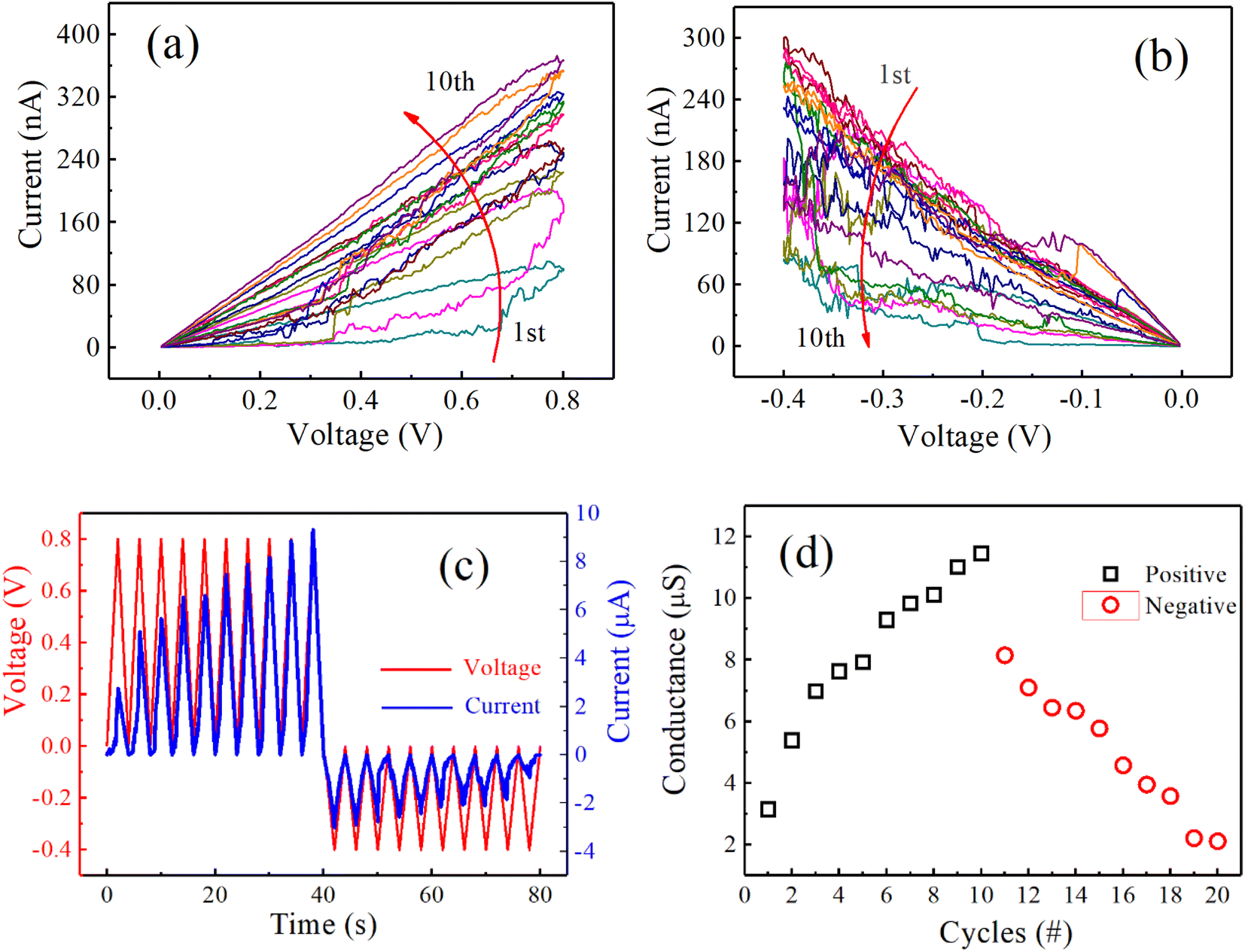 | ||
| Fig. 2 Memristor properties and its simulation as a synapse. Measured I–V properties of the device (a) positive part and (b) negative part. (c) The current and voltage data versus time for the device in (a) and (b) highlighting the change in current in sequential voltage sweeps. (d) Changes of the device conductance during consecutive sweeps. | ||
The conductance can be gradually modulated by applying a series of programmed pulses. As can be seen in Fig. 3, by applying 50 positive pulses (+1 V, 1 ms) and 50 negative pulses (−1 V, 1 ms) to the memristor, it is found that the device conductance continuously increases and decreases. The modulation of conductance can be regarded as a consequence of the migration of Ag ions caused by the electric field.17,25 Based on the memristor, the LTP and LTD behavior of synapses is simulated.
 | ||
| Fig. 3 The device conductance can be gradually increased or decreased by continuous potentiating or depressing pulses. The inset is diagram of 100 pulses. P, 1 V, 1 ms; D, −1 V, 1 ms; R, 0.1 V, 1 ms. | ||
The function of STP is very important to the execution of computational actions in the biological neural system. Which can be imitated through the volatile properties of memristor.16,17 Fig. 4 exhibits the property of volatile threshold switching (TS) in the Ag/Ag:ZnO/Pt device under DC voltage sweeping with very small compliance current (500 nA). When the positive voltage applied on TE of the device, the current increases quickly at the threshold voltage (0.4 V), and then the device switches to the low resistance state (LRS). With the voltage falling below a certain value (0.2 V), the LRS reverses back to original high resistance state (HRS) spontaneously. It can be inferred that the interfacial energy minimization leads to spontaneous fracture of the slim Ag filament, which contributes to the volatile TS property.16 Furthermore, conductive filaments have been found directly by in situ transmission electron microscopy.15,16,26
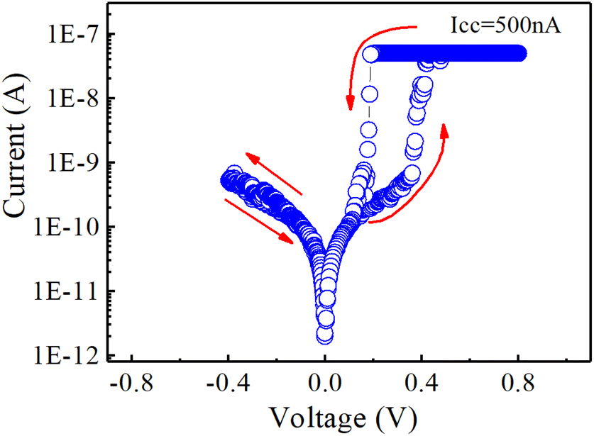 | ||
| Fig. 4 The threshold switching (TS) I–V loops with low compliance current (500 nA). | ||
Fig. 5(a) describes the PPF function in a biological synapse. That is, under the stimulation of two consecutive spikes (orange line), the second postsynaptic response current becomes larger than the first (green line), and the interval between the two spikes is less than the recovery time.17 Similarly, as shown in Fig. 5(b), in our device, the PPF function can be simulated by two continuous pulses (1 V, 1.2 ms) with transient time separation (1 ms). The second response current of stimulus pulse is obvious greater than the first (green line). This is because the relaxation time of Ag atoms in RS layer is longer than the interval time between two sequential pulse stimulations. So the conductance of the device increases accordingly.17
 | ||
| Fig. 5 (a) The diagram of PPF phenomenon in a biological synapse. (b) The PPF property of the device. | ||
While the device is tested under a higher compliance current (CC) of 10 μA, a transition from synaptic simulation to nonvolatile resistive switching behavior can be obtained. It can be seen from Fig. 6(a) that an obvious bipolar resistive switching behavior is observed in the Ag/Ag:ZnO/Pt device. The device current reaches the CC at a voltage of about 0.3 V, and the device switches from the HRS to the LRS. Different from the LRS obtained under a lower CC (500 nA) shown in Fig. 4(a), the conductive LRS obtained under the CC of 10 μA can be maintained even after the imposed positive voltage disappears, which indicates the nonvolatile resistive switching behavior of the Ag/Ag:ZnO/Pt device. Afterwards, by sweeping the voltage from zero to a negative voltage, a sudden drop of the device current can be observed at a reset voltage of about −0.2 V, and the device can be switched back to the HRS. In order to further investigate the effect of the CC on the resistive switching behavior, higher CCs of 25 μA, 50 μA, 100 μA are applied in order. Fig. 6(b)–(d) show the similar typical I–V characteristics of the Ag/Ag:ZnO/Pt device under the next three CCs. Interestingly, different from Fig. 6(a) and (b), a gradual drop of the device current can be observed at a reset voltage of about −0.3 V in Fig. 6(c) and (d), which suggests that the sudden and gradual reset can be converted in a single Ag/Ag:ZnO/Pt device by controlling different CC. These results confirm that Ag+ ions can migrate into ZnO film to form metallic conductive filaments across the oxide film, and thus the device switches between the HRS and the LRS. In addition, the Ag NCs inserted in the ZnO film can enhance the electric field intensity, which facilitates the formation and rupture of the Ag conductive filament and keeps the performance of the device stable, as reported in many previous work.2,6,27
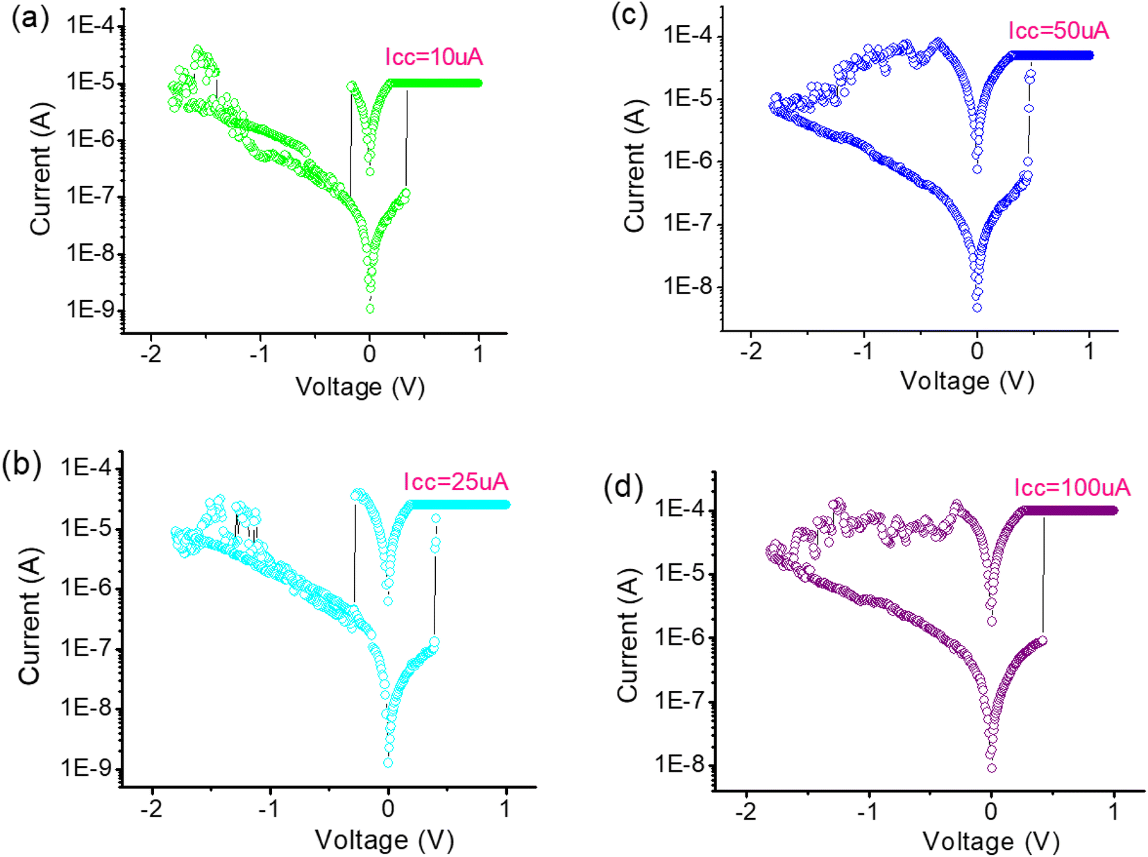 | ||
| Fig. 6 (a)–(d) I–V hysteresis curves with different ICC values for Ag/Ag:ZnO/Pt RRAM device, showing the sharp reset converted to the gradual reset while ICC reached 50 μA. | ||
To investigate the RS parameters of the device under four CCs, the switching voltage, current, and resistance of the HRS and the LRS were analyzed statistically. Fig. 7(a) and (b) show the data of statistic of the RHRS and RLRS, respectively. The data of maximum and minimum fluctuation is obvious. The RHRS value fluctuated as (4170 ± 640 kΩ), (4470 ± 360 kΩ), (1120 ± 90 kΩ), and (540 ± 9 kΩ), and the RLRS value fluctuated as (19.35 ± 2.5 kΩ), (7.75 ± 0.7 kΩ), (6.45 ± 0.5 kΩ), and (2.69 ± 0.1 kΩ) under the four CCs, respectively. As can be seen, generally, the higher the CC imposed on the device, the lower the resistance value in HRS or LRS. And the on/off ratio always kept ∼102. Obviously, the CC plays a significant role in RS characteristic. As CC increases, the conductive filament becomes thicker, and the resistance of LRS decreases. Maybe the conductive filaments can't completely disappear during the reset process, which will also greatly reduce the resistance of HRS. Fig. 7(c) and (d) show the statistic data of Vset/Iset and Vreset/Ireset under the four CCs, respectively. Both Iset and Ireset exhibit an increasing trend when the CC increases, while the Vset and Vreset are only fluctuated in a small range, Vset between 0.3 and 0.4 V and Vreset between −0.2 and −0.4 V, respectively. The measurement results show that the Ag/Ag:ZnO/Pt device can be applied into both synaptic emulation and bipolar resistive switching memory, making us more possible to fabricate a true “thinking machine”.
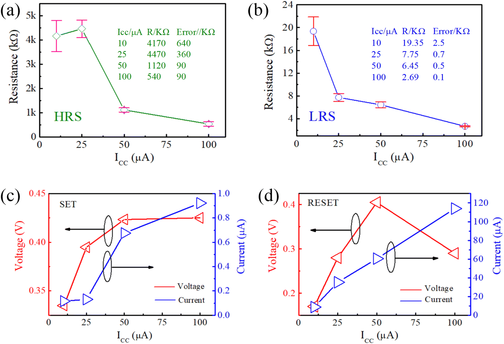 | ||
| Fig. 7 While ICC increased, (a) RHRS and (b) RLRS decreased; (c) Iset and Vset increased; (d) Ireset increased. | ||
In addition, under 100 μA CC, the endurance and retention ability of the device were measured through applying pulse stimuli, as shown in Fig. 8. A series of write/erase cycles stimulated by short pulses, namely, 5 V, 1 ms bias for writing and −5 V, 1 ms bias for erasing, respectively. The measured result of the device is very stable. Which confirms the stability of switching, and showing this switching is feasible for future practical memory application.
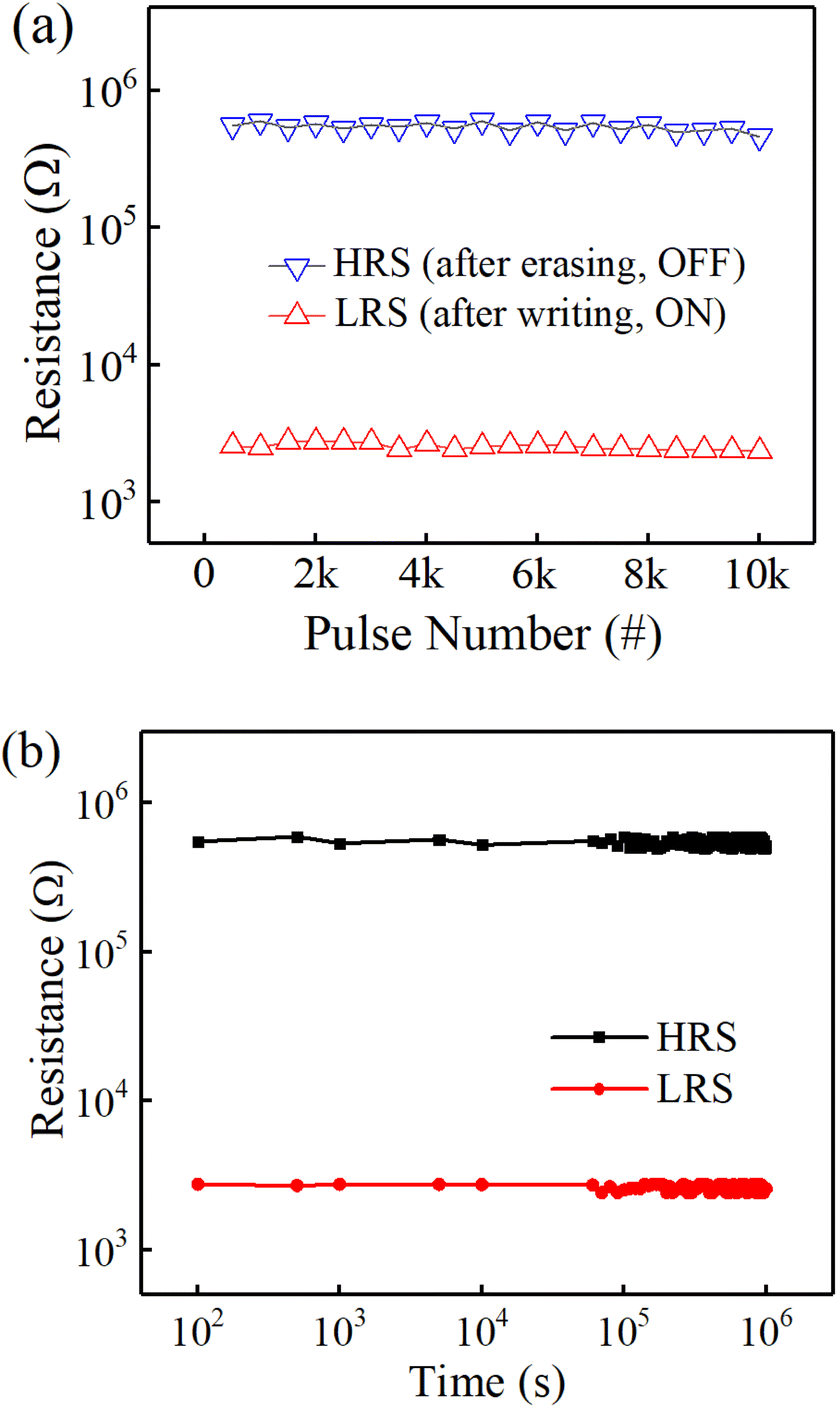 | ||
| Fig. 8 (a) Endurance and (b) retention ability of the device using short pulses (±5 V, 1 ms). | ||
4. Conclusions
In summary, we have verified that synaptic simulation and nonvolatile resistive switching properties were achieved in one device of Ag/Ag:ZnO/Pt through changing compliance current. Several functions of bio-synapse, including nonlinear transmission characteristics, STP, LTP, LTD, PPF were imitated. After increasing the compliance current, the nonvolatile bipolar resistive switching was observed. We can infer that both volatile and nonvolatile switching mechanisms are due to Ag electrochemical metallization and the corresponding formation and rupture of the conductive filaments. The results indicate that the as-fabricated devices possess potential application in the neuromorphic and data storage systems.Conflicts of interest
There are no conflicts to declare.Acknowledgements
This research was funded by the National Natural Science Foundation of China (11804150), the Natural Science Foundation of Jiangsu Province (BK20201111), the Collaborative Education Program of the Ministry of Education of China (202102227001), and the Scientific Foundation of Jinling Institute of Technology (jit-h-2022-218).References
- L. Chua, Memristor-the missing circuit element, IEEE Trans. Circuit Theory, 1971, 18(5), 507–519 Search PubMed.
- M. J. Lee, S. I. Kim, C. B. Lee, H. X. Yin, S. E. Ahn, B. S. Kang, K. H. Kim, J. C. Park, C. J. Kim, I. Song, S. W. Kim, G. Stefanovich, J. H. Lee, S. J. Chung, Y. H. Kim and Y. Park, Low-Temperature-Grown Transition Metal Oxide Based Storage Materials and Oxide Transistors for High-Density Non-volatile Memory, Adv. Funct. Mater., 2009, 19(10), 1587–1593 CrossRef CAS.
- H. S. P. Wong, H. Y. Lee, S. M. Yu, Y. S. Chen, Y. Wu, P. S. Chen, B. Lee, F. T. Chen and M. J. Tsai, Metal-Oxide RRAM, P IEEE, 2012, 100(6), 1951–1970 CAS.
- Q. T. Wu, W. Banerjee, J. C. Cao, Z. Y. Ji, L. Li and M. Liu, Improvement of durability and switching speed by incorporating nanocrystals in the HfOx based resistive random access memory devices, Appl. Phys. Lett., 2018, 113, 023105 CrossRef.
- S. Gora, L. Thyda, G. Dasi, R. Muniramaiah, A. Thakre, J. Gangwar, D. P. Joseph, M. Kovendhan, P. A. Azeem, D. Dinakar, K. Thangaraju and H. Borkar, Asymmetric resistive switching by anion out-diffusion mechanism in transparent Al/ZnO/ITO heterostructure for memristor applications, Surf. Interfaces, 2022, 30, 101950 CrossRef CAS.
- Y. Huang, J. Zhou, Y. Huang and R. Wang, Improvement of durability by incorporating nanocrystals in ZnO-based resistive random access memory devices, Semicond. Sci. Technol., 2020, 35(8), 085031 CrossRef CAS.
- M. Asif and A. Kumar, Existence of bipolar and unipolar resistive switching in CaZrO3 thin film device, J. Alloys Compd., 2021, 859, 158373 CrossRef CAS.
- H. Borkar, A. Thakre, S. S. Kushvaha, R. P. Aloysius and A. Kumar, Light assisted irreversible resistive switching in ultra thin hafnium oxide, RSC Adv., 2015, 5(44), 35046–35051 RSC.
- S. G. Kim, J. S. Han, H. Kim, S. Y. Kim and H. W. Jang, Recent Advances in Memristive Materials for Artificial Synapses, Adv. Mater. Technol., 2018, 3, 1800457 CrossRef.
- I. Boybat, M. Le Gallo, S. R. Nandakumar, T. Moraitis, T. Parnell, T. Tuma, B. Rajendran, Y. Leblebici, A. Sebastian and E. Eleftheriou, Neuromorphic computing with multi-memristive synapses, Nat. Commun., 2018, 9, 2514 CrossRef PubMed.
- D. Ielmini, Brain-inspired computing with resistive switching memory (RRAM): devices, synapses and neural networks, Microelectron. Eng., 2018, 190, 44–53 CrossRef CAS.
- L. Y. Wang, Z. Y. Wang, W. Zhao, B. Hu, L. H. Xie, M. D. Yi, H. F. Ling, C. X. Zhang, Y. Chen, J. Y. Lin, J. L. Zhu and W. Huang, Controllable Multiple Depression in a Graphene Oxide Artificial Synapse, Adv. Electron. Mater., 2017, 3, 1600244 CrossRef.
- L. G. Wang, W. Zhang, Y. Chen, Y. Q. Cao, A. D. Li and D. Wu, Synaptic Plasticity and Learning Behaviors Mimicked in Single Inorganic Synapses of Pt/HfOx/ZnOx/TiN Memristive System, Nanoscale Res. Lett., 2017, 12, 65 CrossRef PubMed.
- X. B. Yan, J. J. Wang, M. L. Zhao, X. Y. Li, H. Wang, L. Zhang, C. Lu and D. L. Ren, Artificial electronic synapse characteristics of a Ta/Ta2O5−x/Al2O3/InGaZnO4 memristor device on flexible stainless steel substrate, Appl. Phys. Lett., 2018, 113, 013503 CrossRef.
- X. Yan, J. Zhao, S. Liu, Z. Zhou, Q. Li, J. Chen and X. Y. Liu, Memristor with Ag-Cluster-Doped TiO2 Films as Artificial Synapse for Neuroinspired Computing, Adv. Funct. Mater., 2018, 28, 1705320 CrossRef.
- Z. Wang, S. Joshi, S. E. Savel'ev, H. Jiang, R. Midya, P. Lin, M. Hu, N. Ge, J. P. Strachan, Z. Li, Q. Wu, M. Barnell, G.-L. Li, H. L. Xin, R. S. Williams, Q. Xia and J. J. Yang, Memristors with diffusive dynamics as synaptic emulators for neuromorphic computing, Nat. Mater., 2017, 16(1), 101–108 CrossRef CAS PubMed.
- X. Zhang, S. Liu, X. Zhao, F. Wu, Q. Wu, W. Wang, R. Cao, Y. Fang, H. Lv, S. Long, Q. Liu and M. Liu, Emulating Short-Term and Long-Term Plasticity of Bio-Synapse Based on Cu/a-Si/Pt Memristor, IEEE Electron Device Lett., 2017, 38(9), 1208–1211 CAS.
- Y. Park and J. S. Lee, Artificial Synapses with Short- and Long-Term Memory for Spiking Neural Networks Based on Renewable Materials, ACS Nano, 2017, 11(9), 8962–8969 CrossRef CAS PubMed.
- Y. Huang, Z. H. Shen, Y. Wu, X. Q. Wang, S. F. Zhang, X. Q. Shi and H. B. Zeng, Amorphous ZnO based resistive random access memory, RSC Adv., 2016, 6(22), 17867–17872 RSC.
- S. S. Peng, F. Zhuge, X. X. Chen, X. J. Zhu, B. L. Hu, L. Pan, B. Chen and R. W. Li, Mechanism for resistive switching in an oxide-based electrochemical metallization memory, Appl. Phys. Lett., 2012, 100, 072101 CrossRef.
- S. A. Khan, G. H. Lee, C. Mahata, M. Ismail, H. Kim and S. Kim, Bipolar and complementary resistive switching characteristics and neuromorphic system simulation in a Pt/ZnO/TiN synaptic device, Nanomaterials, 2021, 11(2), 315 CrossRef CAS PubMed.
- W. Banerjee, Q. Liu, S. Long, H. Lv and M. Liu, Crystal that remembers: several ways to utilize nanocrystals in resistive switching memory, J. Phys. D: Appl. Phys., 2017, 50(30), 303002 CrossRef.
- Y.-X. Hou, Y. Li, Z.-C. Zhang, J.-Q. Li, D.-H. Qi, X.-D. Chen, J.-J. Wang, B.-W. Yao, M.-X. Yu, T.-B. Lu and J. Zhang, Large-Scale and Flexible Optical Synapses for Neuromorphic Computing and Integrated Visible Information Sensing Memory Processing, ACS Nano, 2021, 15(1), 1497–1508 CrossRef CAS.
- J. Zhu, T. Zhang, Y. Yang and R. Huang, A comprehensive review on emerging artificial neuromorphic devices, Appl. Phys. Rev., 2020, 7, 011312 CAS.
- W. Wang, G. Pedretti, V. Milo, R. Carboni, A. Calderoni, N. Ramaswamy, A. S. Spinelli and D. Ielmini, Learning of spatiotemporal patterns in a spiking neural network with resistive switching synapses, Sci. Adv., 2018, 4, eaat4752 CrossRef CAS PubMed.
- Y. C. Yang, F. Pan, Q. Liu, M. Liu and F. Zeng, Fully Room-Temperature-Fabricated Nonvolatile Resistive Memory for Ultrafast and High-Density Memory Application, Nano Lett., 2009, 9(4), 1636–1643 CrossRef CAS PubMed.
- W. Chen, H. J. Barnaby and M. N. Kozicki, Volatile and Non-Volatile Switching in Cu–SiO2 Programmable Metallization Cells, IEEE Electron Device Lett., 2016, 37(5), 580–583 CAS.
| This journal is © The Royal Society of Chemistry 2022 |