DOI:
10.1039/D2RA05430B
(Paper)
RSC Adv., 2022,
12, 29666-29676
Structural, optical, and magnetic properties of Ag+, Mn+ and Ar+ ions implanted ZnO thin films: effect of implantation dose and stopping energy†
Received
30th August 2022
, Accepted 10th October 2022
First published on 18th October 2022
Abstract
Herein, we systematically studied the effect of various excitation processes on the structural, optical, and magnetic properties of ZnO films implanted with 80 keV Ar+, 110 keV Mn+, and 190 keV Ag+ ions. Four different doses of 1 × 10¹³, 1 × 10¹⁴, 1 × 10¹⁵, and 2 × 10¹⁶ ions per cm2 were used for implantation. It was observed that the structural, optical, and magnetic properties of the implanted samples were dominantly affected at the highest dose of 2 × 10¹⁶ ions per cm2. For lower doses, insignificant changes in these properties were observed. A comparison of various processes involved in the implantation process shows that both the electronic excitation and nuclear excitation processes are responsible for the changes in the structural, optical, and magnetic properties of the implanted ZnO films.
Introduction
The presence of magnetism in semiconductors provides an alternative to overcome the technical limitations of conventional Si-based semiconductors and allows them to be used in the field of spintronics.1–3 Spintronic materials for applications must be highly spin polarizable and should possess ferromagnetism (FM) with a Curie temperature above room temperature.4–6 In general, spintronic materials do not exhibit ferromagnetism without unpaired electrons, so the most common method for these materials to have ferromagnetism above room temperature is to introduce transition metal elements with unpaired electrons such as V, Mn, Cr, Fe, or Co.7–9 However, Venkatesan et al. reported ferromagnetism in HfO2 thin films without magnetic elements.10 This finding opened up a new field of “magnetism without unpaired electrons” in the scientific community, which is sometimes also referred to as defect-induced magnetism.
Among the various non-magnetic oxides in this category, ZnO is an important material which is widely used in various applications, including optoelectronic materials, chemical sensors, and solar cells.5,6,11–14 ZnO is also extensively studied for its use as a spintronic material as well as for understanding the origin of magnetism.15–19 As a whole, this material has ferromagnetic properties when the magnetic dopants are substituted into cation sites.7–9 This behavior is known to be the result of the exchange interaction between localized magnetic moments and electronic spin moments resulting from defects such as oxygen vacancies and Zn interstitials at the surface of ZnO thin films.15–22 It is further shown that defects are required to induce magnetism in these oxides.23,24 Thus, to understand such a phenomenon, it is necessary to investigate the effect of defects on the ferromagnetic properties of ZnO thin films by intentionally creating external defects.
In case of external defects, it is most important to distribute them evenly.25 This requirement can be fulfilled by ion implantation method as it has excellent ability to create defects and spread the dopant uniformly over a selected area.26 In addition, this method allows easy control of the concentration of dopants in the target materials. Unlike other methods, it has the advantage of removing the contamination of unknown external elements because the dopant introduced into the material is highly mass selective in a vacuum chamber.
The factors that play a key role in determining the characteristics of the implanted materials are the implantation dose, energy, and type of dopant. The number of defects is influenced by the amount of energy transferred to the medium by implanted ions, i.e., the energy loss of the incident ions. This energy is the so-called “stopping power”, and the larger this energy, the more defects are generated in the film.27 This energy also determines the doping depth in the film. In this manner, dopant ions play a dominant role in determining the magnetic behaviors of the host system, which is considered to be an interplay between the defects and nature of dopant.28,29
In this study, the implantation was performed using three kinds of ions to systematically investigate the role of defects on various properties of ZnO. The first element is Mn, a transition metal typically used to make ferromagnetic materials, because it has unpaired d-orbital electrons. The second element is Ar that has no d-orbital electrons required to establish the role of unpaired d-orbital electrons. The third element is Ag, which has larger atomic size than Mn and Ar, and has no unpaired d-orbital electrons. The nature of defects/vacancies was identified by means of UV-Visible spectroscopy, photoluminescence (PL) spectroscopy, and synchrotron radiation X-ray absorption spectroscopy (XAS). To probe the local magnetic moment, X-ray magnetic circular dichroism (XMCD) measurements were carried out. Consequently, attempts were made to relate the nature of defects, local magnetic moments, and the magnetic behavior of ZnO.
Experimental details
Growth of ZnO thin films
Quartz and sapphire substrates were employed to deposit ZnO thin films at substrate temperature of 100 °C using radio-frequency (RF) magnetron sputter with a 2-inch ZnO target (99.99% purity). For XMCD measurements, a sapphire substrate was used, but most of the measurements were performed on quartz. In addition, highly crystalline ZnO thin films were grown on both the substrates and had similar strain and grain sizes.30,31 The detailed RF magnetron sputter deposition of ZnO films was given in our previous paper.23 The quartz and sapphire substrates (size: 7 × 7 mm2) were ultrasonically treated in cleaning agents for 5 min per step and blow-dried with N2 gas before loading in the deposition chamber. During the deposition of ZnO films, the working pressure was kept at 5.0 × 10⁻³ Torr. The mixture of high purity O2 and Ar gases (O![[thin space (1/6-em)]](https://www.rsc.org/images/entities/char_2009.gif) :Ar = 1:10) was employed as sputter gas. The sputtering power was fixed at 75 W. The substrate was rotated with 6.5 rpm to obtain a uniform deposition of ZnO films.
:Ar = 1:10) was employed as sputter gas. The sputtering power was fixed at 75 W. The substrate was rotated with 6.5 rpm to obtain a uniform deposition of ZnO films.
Implantation of Ar+, Mn+ and Ag+
Implantation of Ar+, Mn+, and Ag+ ions was conducted with Cockroft–Walton type 400 kV ion beam accelerator (High Voltage Engineering Europa B.V.) installed at Korea Institute of Science and Technology (KIST), Korea. The implantation energies of Ar+, Mn+, and Ag+ were 80, 110, and 190 keV, respectively, and the dose of 1 × 10¹³, 1 × 10¹⁴, 1 × 10¹⁵, and 2 × 10¹⁶ ions per cm2 was used (Table 1). The energies are chosen to locate the dopants at similar specific depth in the ZnO films. The projected range, straggling, stopping values (Table 2), and the distribution profiles of these implanted ions in sapphire and quartz substrates were calculated with the Stopping and Range of Ions in Matter (SRIM) calculation.32 After implantation, the films were annealed at 400 °C for 60 min in an Ar gas environment.23
Table 1 Implantation conditions: ions, energy and dose for implantation in ZnO films. Projected range (Rp) and straggling values estimated from SRIM is also collated
| Deposited thin films |
Substrate |
Ions |
Energy (keV) |
Dose (ions per cm2) |
Rp (Å) |
Straggling (Å) |
| Longitudinal |
Lateral |
| ZnO |
Quartz, sapphire |
Ar+ |
80 |
1 × 10¹³, 1 × 10¹⁴, 1 × 10¹⁵, 2 × 10¹⁶ |
490 |
233 |
166 |
| Mn+ |
110 |
513 |
228 |
158 |
| Ag+ |
190 |
476 |
164 |
161 |
Table 2 Stopping values, S (keV μg−1 cm−2), for Ar+ (80 keV), Mn+ (110 keV) and Ag+ (190 keV) ions in ZnO films
| |
Ar |
Mn |
Ag |
| dE/dx (nuclear), Sn |
1.56 |
2.52 |
5.94 |
| dE/dx (electronic), Se |
0.581 |
0.392 |
0.794 |
| Se/Sn |
0.374 |
0.156 |
0.134 |
| Sn/Se |
3.88 |
6.42 |
7.48 |
| Sn + Se |
2.14 |
2.91 |
6.73 |
| Atomic radii (nm) |
0.71 |
1.40 |
1.65 |
Characterizations
Rutherford backscattering spectrometry (RBS) measurements were performed with 6SDH-2 Pelletron Accelerator (National Electronic Corporation) installed at KIST. These RBS spectra were simulated using the RUMP program for the estimation of film thickness.33 Structural studies were performed with D8-Advance X-ray diffractometer using Cu-Kα radiation (λ = 1.541 Å). XAS examinations at Zn K-edge were made with 1D XRS KIST-PAL beamline at Pohang Accelerator Laboratory, Korea. The detailed information about examinations was provided elsewhere.34 To calculate the XAS spectra, several paths were selected from the ZnO structural information file with ATOMs.35 These paths in the R-range of 1–3.5 Å were considered for calculation, and the best fitted spectra were attained. Photoluminescence spectra and UV-Visible spectroscopic data in a 200–800 nm wavelength range were measured. Near edge X-ray absorption fine-structure (NEXAFS) measurements at Zn L- and O K-edges were made in total electron yield (TEY) and total fluorescence yield (TFY) modes at the 10D XAS KIST beamline.34,36 Magnetic assessment was done with a Magnetic Property Measurement System. The O K-edge XAS assessment was performed under different helicity of circularly polarized light at 2A MS beamline to acquire an XMCD signal.36
Results and discussion
Initial investigations
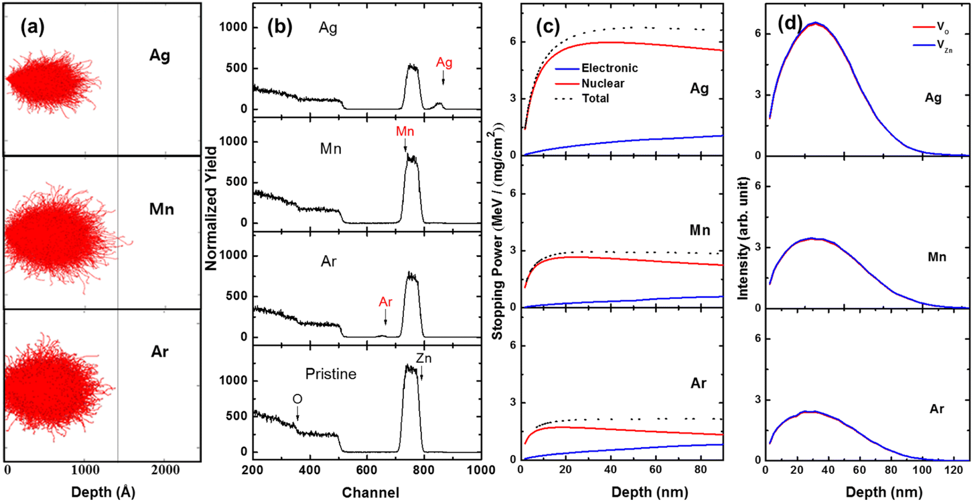
First, the behavior of implanted ions in ZnO films (thickness of 138 nm) was investigated using SRIM calculation. Fig. 1a exhibits the trajectories of Ar+, Mn+ and Ag+ ions in the ZnO films, showing the localization of implanted ions within the films. Since each dopant has different energy to be located at the same specific depth in the ZnO films, the shape of the implanted Ag+ profile with the highest energy is sharper than those of other dopants. The presence of these dopants in the ion-implanted films is confirmed by the RBS spectra (Fig. 1b). The results clearly show the presence of dopants in ZnO thin films at the highest dose. The film thickness appears to remain almost the same, unaffected by the difference in implanted ion doses, but it actually decreases at particularly higher doses. It is shown that Ag, having larger size than other elements, has a relatively large thickness reduction (Table S1†). The thickness reduction at higher doses is due to implantation-induced sputtering.37,38 These results can also be predicted through energy deposition in the form of nuclear and electron excitation of ions using SRIM calculation (Fig. 1c). Moreover, the SRIM calculations show that Ag+ ion has the highest energy deposition via nuclear excitation. (Fig. S1†). The dominant nuclear excitation process loses energy in the form of cascades, which results in the generation of oxygen vacancies (VO), zinc vacancies (VZn) and/or atomic displacement (Fig. 1d).39
 |
| | Fig. 1 Implantation characteristics of ions: (a) Schematic of the trajectories of Ar+, Mn+ and Ag+ ions in ZnO, showing that ions reside within the film region only. (b) RBS spectra of implanted films at the highest dose confirming the presence of implanted ions. (c) Stopping power (S, dotted black), electronic stopping power (Se, blue) and nuclear stopping power (Sn, red line) as a function of penetration depth in ZnO films. (d) VO and VZn produced by implanted ions in the films. | |
Structural study
Generation of VO and VZn along with atomic displacements as determined by SRIM calculation can affect the unit cell. Hence, the effects of these factors on various structural parameters were investigated using X-ray diffraction (XRD) (Fig. 2). Fig. 2a reveals the XRD patterns of the pristine and implanted films at the highest dose (2 × 10¹⁶ ions per cm2) for Ag+, Mn+, and Ar+ ions. The strong diffraction peak of pristine film corresponds to the (002) plane of wurtzite structure having P63mc space group.40 For the implanted samples, the strong diffraction peaks without additional peaks indicate that each dopant well occupied the Zn sites.41,42 The origin of the peak (103) is not clear, but it can be related to the surface nature of ZnO films. A detailed discussion about this peak has been carried out in previous report of our group.23 The two peaks in the XRD patterns of the implanted films imply the occurrence of the same structure after implantation. Since radiation damage is common in implanted systems, XRD patterns of the implanted films at various doses were further analyzed. The XRD patterns show that the intensity decreases with increasing dose of Ar+ (Fig. S2†), Mn+ (Fig. S3†) and Ag+ ions (Fig. S4†). To better understand this behavior, the XRD peak corresponding to the (002) plane is illustrated in Fig. 2b. It is evident that the peak intensity reduces significantly for high dose of implantation. A reduction in XRD peak intensity is related to a decrease in the degree of crystallinity,43 which is commonly observed in implanted oxide materials as a result of damage induced by implanted ions.44 Apart from the change in intensity, a visual inspection shows a shift in peak position. So, the shift in peak positions as a function of implantation dose is illustrated in Fig. 2c. The shift is associated with stress developed in the system caused by the presence of the implanted ions in the lattice.45 Fig. 2c reveals both the dose and atomic size dependence as indicated by the dotted rectangular regions. At low doses, an insignificant shift in the peak position is observed. At moderate doses, almost the same shift is observed for Mn+ and Ag+ ions, while for the Ar+ ion implanted film, no shift is seen compared to the low does. At high doses, the peak shift significantly depends on the atomic size. For Ag+ ions having an atomic radius of 1.65 Å, a large positive shift is observed, while Mn+ ions having atomic radius of 1.40 Å, a moderate shift is shown. This may be due to the reduced ionic radii of Mn ion states because the implanted Mn+ ions in ZnO exist as 3+ oxidation state (but not as Mn+) as shown in Fig. S5.† For Ar+ ions (atomic radius ∼0.72 Å) a negative shift is observed. If different peak shifts are observed for ions with the similar atomic radii, this may be due to the different valence states of these ions because the ionic radii vary with the valence states. The influence of these ions on the lattice was determined by calculating lattice parameters ‘a’ and ‘c’ from the relation as depicted in ESI text S1.† The lattice parameter is expected to depend on both the implantation dose and ion size. However, lattice parameter dependence reveals a trend opposite to the peak shift (Fig. 2d). As evident from the peak shift, the presence of higher stress causes lattice shrinkage, resulting in the reduction in parameter ‘c’ for the Ag+ and Mn+ ion-implanted samples.27,45 However, lattice expansion is observed in Ar+ ion implanted samples.46 Further, the variation in crystallite size according to the implantation dose was estimated. For all ions, crystallite size is maximum at 1 × 10¹³ ions per cm2 and then decreases with increasing implantation dose.45 Thus, the crystallite size is dominantly affected by the implantation dose. The effect of the atomic size of the implanted ions on the crystallite size is insignificant. This may be related to the formation mechanism of crystallite that was governed by the energy deposited in the system rather than the radii of the implanted ions causing lattice expansion/contraction.
 |
| | Fig. 2 Structural properties: (a) XRD patterns of the films before and after implantations with Ar+, Mn+ and Ag+ ions (the highest dose only). (b) (002) XRD peaks at various doses for all ions. Variation of (c) peak position, (d) lattice parameter and (e) crystallite size with implantation dose for Ar+, Mn+ and Ag+ ions. (f) k2-Weight EXAFS spectra at different implantation doses for Ar+, Mn+ and Ag+ ions. | |
An amount of excessive energy in the system causes damage, resulting in a decrease in the crystallite size.47 So, this effect is dominant at high implantation doses. Because both the lattice and crystallites are affected by implanted ions, their effects on the local atomic structures were also investigated by extended X-ray absorption fine structure (EXAFS) measurements on the films implanted by Ar+ (Fig. S6†), Mn+ (Fig. S7†) and Ag+ (Fig. S8†) ions. k2-weighted χ(k) EXAFS spectra of the ZnO films at different doses are presented in Fig. 2f. At all doses, oscillations in the spectra are similar to each other, revealing the same kind of local atomic structure in both the pristine and implanted films.23 This implies that energy deposited in the thin film is not high enough to manifest the local atomic structure, but the evolution of vacancies and point defects cannot be ruled out in the implanted films as noted from the SRIM calculation (Fig. 1d). Thus, both crystallite size and lattice parameter exhibit significant changes at the highest dose. This may be caused by factors, including large amounts of implanted ions in the lattice and the energy transferred to the lattice. Since nuclear stopping is well known to play a vital role in the case of implantation, the behavior of structural parameters was described as functions of ionic radii, nuclear stopping (Sn)/electronic stopping (Se), and Sn + Se (Fig. 3). The crystallite size of these films does not reveal any relationship with the ionic radii, Sn/Se and Sn + Se (Fig. 3a). However, changes in the lattice parameters show a linear behavior in Sn + Se. This indicates that the unit cell is affected by the total energy transferred to the lattice.
 |
| | Fig. 3 Structural parameters and energy loss: (a) crystallite size and (b) changes in lattice parameters as functions of ionic radii, nuclear stopping/electronic stopping (Sn/Se) and total electronic energy loss (Sn + Se). | |
Morphological study
To examine the influence of implantation doses on the surface of ZnO films, atomic force microscope (AFM) measurements were performed. AFM images for the pristine and implanted films at the highest dose are shown in Fig. 4. A visual inspection shows the surface modification in the implanted samples, depending on the type of implanted ions (Fig. 4a). AFM images at different doses for Ar+ (Fig. S9†), Mn+ (Fig. S10†), and Ag+ (Fig. S11†) exhibit dose-dependent changes in the surface morphology. The surface roughness of the samples implanted with different doses is shown in Fig. 4b. The RMS roughness of the pristine ZnO film is 2.126 nm. The roughness varies with increasing implantation doses. The Ar+ ion-implanted sample exhibits random variations with implantation doses, whereas a systematic variation is found in the Mn+ and Ag+ ion-implanted samples. With increasing implantation dose, the roughness for the Mn+ and Ag+ ion-implanted samples decreases up to 1 × 10¹³ ions per cm2 and then increases. At the highest dose (2 × 10¹⁶ ions per cm2), a huge increase in the roughness (i.e., 3.707 and 5.875 nm) is observed for Mn+ and Ag+ ions, respectively.48 These values with ionic radii (Fig. S12†) and Sn/Se (Fig. S12†) show the same variation, while the variation with Sn + Se is almost linear (Fig. 4c) at the highest dose (2 × 10¹⁶ ions per cm2).
 |
| | Fig. 4 Surface morphology: (a) AFM images of ZnO films before and after implantations with Ar+, Mn+ and Ag+ ions at 2 × 10¹⁶ ions per cm2. RMS roughness as a function of (b) implantation dose and (c) Sn + Se at the highest dose. | |
Optical behaviour
To elucidate the effect of implanted ions on the optical behavior, UV-Visible spectra at different doses of Ag+, Mn+, and Ar+ ions were analyzed (Fig. 5). Analogous to the structural and morphological behaviors, the optical properties are also influenced by both the implantation dose and the kind of ions. The shape of UV-Visible spectra exhibits an insignificant change and is not affected by the nature of implanted ions up to the dose of 1 × 10¹⁵ ions per cm2 (Fig. 5a). However, the shape of the spectra is affected by the nature of ions at 2 × 10¹⁶ ions per cm2. Tauc's plots (Fig. 5b) are estimated from the absorption spectra (Fig. 5a) using the relation given in literature.23
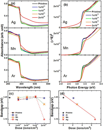 |
| | Fig. 5 Optical behavior: (a) UV-visible spectra and (b) Tauc's plots of Ar+, Mn+ and Ag+ ions-implanted ZnO films at various doses. (c) Optical bandgap of the implanted films as a function of implantation dose. (d) Optical bandgap for the highest dose as a function of total energy loss (Sn + Se). | |
The Tauc's plots are used to determine the optical bandgap by the method depicted in Fig. S13.† The optical bandgap of the pristine film is 3.20 eV.49 Despite the different kinds of implanted ions, their bandgaps remain almost unchanged (within experimental error) up to 1 × 10¹⁵ ions per cm2 (Fig. 5c). At 2 × 10¹⁶ ions per cm2, the optical bandgap is estimated to be 3.19, 3.17, and 3.09 eV for Ar+, Mn+ and Ag+ ions, respectively (Fig. 5c). A similar reduction in the optical bandgap was also observed in the ZnO nanowires,50 where the origin of the bandgap reduction is attributed to structural modification caused by the implanted ions. In our study, the dominant reduction was found at the highest dose in the Ag+ ion-implanted ZnO films, which is related to the highest damage as shown in Fig. 1d. Analogous to variations of other parameters, the optical bandgap displays a linear variation with Sn + Se (Fig. 5d), but not with ionic radii and Sn/Se (Fig. S14†).
Magnetic study
The magnetic behavior of the samples was investigated by measuring magnetic hysteresis (M–H) curves at 300 K (Fig. 6a) and 80 K (Fig. 6b). All curves are saturated with a well-defined and small value of coercivity, showing the magnetic characteristics of the samples. The pristine and implanted films show similar behavior. However, the magnitude of both the saturated magnetization and coercivity depends on the doses and ions. Fig. 6c reveals the saturated magnetization for different ions as a function of the implantation dose.
 |
| | Fig. 6 Magnetic behavior: M–H curves for Ar+, Mn+ and Ag+ ions-implanted films at (a) 300 K and (b) 80 K. (c) Saturation magnetization of the implanted films as functions of implantation dose and ionic radii at 300 and 80 K. | |
At both temperatures, the saturated magnetization decreases with dose of Ar+ ion implantation. In the case of Mn+ and Ag+ ions, the saturation magnetization increases exponentially with implantation dose. It is noted that unlike Ag, Mn has unpaired d-orbital electrons. Nevertheless, magnetism similarly increases in both the Mn+ and Ag+ implanted ZnO films. This may be associated with the atomic radius. In other words, Ar has smaller atomic size than Zn, so it has less impact on the production of internal defects. However, since Mn and Ag atoms have relatively larger atomic size than Zn, Mn+ and Ag+ cause higher increase in internal defects than Ar+, and thus may increase the saturation magnetization. Further, the ion radius is related to energy transfer and their relationship is displayed in Fig. 6 and S15.† At both temperatures, no linear relationship is observed either with ionic radii (Fig. 6c) or Sn/Se (Fig. S15†). The change in the magnetization exhibits a linear relationship with Sn + Se (Fig. S16†). These films exhibit structural and magnetic characteristics that are affected by both implantation doses and the nature of ions. At the highest dose, a major change in magnetization is observed. To find the atomistic origin of magnetization observed in the implanted ZnO films, XMCD measurements were performed on O K-edge at 80 and 300 K. The NEXAFS spectra at O K-edge were collected in TEY mode for the pristine and Ar+, Mn+, Ag+ implanted ZnO films using left (μL) and right (μR) circularly polarized X-ray beam. All these spectra are shown in the upper panel of Fig. S17–S20.† The XMCD signal (μL − μR)/(μL + μR) is shown at the lower panel of the corresponding NEXAFS spectra (Fig. S17–S20†). The feature observed between 530–545 eV in the O K-edge NEXAFS spectra is related to the electron excitation from O 1s states to 2p states and the intensities are proportional to the density of unoccupied 2p states.51 Although the NEXAFS spectra for the ZnO films before and after implantation are found to almost overlap each other when measured using left and right circularly polarized X-ray, a weak XMCD signal is observed. Thus, the weak XMCD signals confirm that the magnetic moment at O sites is due to the faulty alignment of the spin moments on the surfaces of the pristine and implanted ZnO films.52 These imperfections in the spin moments could be related to the presence of VZn at the film surface.
NEXAFS study
The presence of vacancies and replacement of ions were explored with XAS measurements (Fig. 7). The O K-edge NEXAFS spectra in TEY and TFY modes exhibit the same kinds of spectral features for the implanted ions of Ar+, Mn+, and Ag+. These features are characteristics of ZnO. As for the surface sensitive TEY mode, O K-edge spectral peaks at 538 and 541 eV display changes in the intensity with the implantation dose (Fig. 7a).
 |
| | Fig. 7 Local electronic structure: O K-edge NEXAFS spectra for the implanted ZnO films at various doses with (a) TEY and (b) TFY mode. (c) Zn K-edge NEXAFS spectra at various doses, showing spectral features a1, b1 and c1. | |
However, this kind of effect cannot be observed in bulk sensitive TFY mode NEXAFS spectra (Fig. 7b). The change in the intensity of the spectral features of TEY mode NEXAFS spectra may be associated with the modifications of surface states with implantation dose in these ions (Fig. 7a). The surface modification of these films is also evident from the AFM results. The oxidation state of Zn2+ ions was determined in the implanted films by measuring Zn K-edge NEXAFS spectra (Fig. 7c). The implanted films exhibit the same value of main-edge as that of the pristine, which is 9661 eV (Table S2†). This shows that the zinc oxidation state is not influenced by the implantation process. Moreover, the shape of various spectral features remains unchanged, indicating similar coordination in all samples. This is also seen by the TEY (Fig. S21a†) and TFY (Fig. S21b†) mode Zn L-edge NEXAFS spectra since the spectral features are not modified with ion implantation.
Defects in implanted films
As evidenced by the O K-edge NEXAFS spectra, vacancies were further examined by the PL spectroscopic study of Ar+ (Fig. S22†), Mn+ (Fig. S23†), and Ag+ (Fig. S24†) ions. De-convoluted spectra for these ion-implanted ZnO films are shown in Fig. 8a. Deconvolution was performed by considering peaks at 2.1, 2.2, 2.8 and 3.1 eV.53 A detailed analysis was given in our group's recent work.23 To get information about vacancies, the area of a particular vacancy was divided by the total area of the curve. Fig. 8b reveals the obtained area ratio as a function of the implantation dose for Ag+, Mn+ and Ar+ ions. The area ratio of VZn increases with increasing implantation dose for all ions. Meanwhile, the area ratio of VO decreases with implantation dose of Ar+ and Ag+ ions, but increases for Mn+ ion. Thus, one can see that the number of VO and VZn varies with both implantation doses and kind of ions.
 |
| | Fig. 8 PL study: (a) deconvolution of PL spectra of Ar+, Mn+ and Ag+ ions-implanted films at different doses. Red peaks correspond to VO and sky blue ones to VZn. (b) Area ratio corresponding to VZn (upper panel) and VO (lower panel) for implanted films at various doses. | |
To further study the presence of VO and VZn, EXAFS spectra were simulated to estimate the coordination number of Zn–Zn and Zn–O shells. Simulated k-weight EXAFS spectra are shown in Fig. S25† (Ar+ ion), Fig. S26† (Mn+ ion) and Fig. S27† (Ag+ ion). The simulated non-phase corrected Fourier Transform of EXAFS spectra of implanted ZnO films are shown in Fig. 9a. The simulated parameters are presented in Table S3† (Ar+ ions), Table S4† (Mn+ ions), and Table S5† (Ag+ ions). The coordination numbers corresponding to Zn–Zn and Zn–O shells are shown in Fig. 9b. Irrespective of implantation doses and ions, their coordination numbers are almost similar within small fluctuations. This is indicative of the small variation of Vo and VZn in localized structures with implanted ions and doses.
 |
| | Fig. 9 Local atomic structure: (a) simulation of non-phase corrected Fourier transform of EXAFS spectra for Ar+, Mn+ and Ag+ ions-implanted films. (b) Variation of coordination numbers of Zn–O (upper panels) and Zn–Zn (lower panels) shells as a function of implantation dose. | |
Conclusions
In this study, various characterization techniques, including synchrotron radiation, were employed to comprehend the Ag+, Mn+, and Ar+ ion implantation-induced effects on the structural, optical, and magnetic features of the ZnO film. The role of implantation dose and ionic radii in these effects was also examined. XRD results showed that lattice strain was controlled not only by the dose but also by the ionic radius, and exhibited the maximum strain at the highest implantation dose. Similar behavior was also observed for the lattice constant and crystallite size. Surface roughness of these films was also modified with implantation dose. It was found that the Ag+ ion implanted samples displayed the largest change in the optical bandgap and magnetization at the highest dose. The dependence of the implantation doses and ionic radii showed that the summation of electronic and nuclear energy losses (i.e., total energy loss) in the films is responsible for the changes in the structural, optical, and magnetic characteristics of ZnO films. This imply that both the nuclear and electronic excitation processes mainly contribute to the ion implantation-induced effects on the properties of the ZnO thin films.
Author contributions
Weon Cheol Lim: conceptualization, validation, investigation, writing – original draft. Jitendra Pal Singh: investigation, writing – editing. Jonghan Song: investigation, formal analysis. Tae-Yeon Seong: supervision, writing – review & editing, project administration. Keun Hwa Chae: writing – review & editing, project administration.
Conflicts of interest
There are no conflicts to declare.
Acknowledgements
This work was supported by Korea Institute of Science and Technology (KIST Project No. 2V09190) and the National Research Foundation of Korea (NRF) grant funded by the Korea government (MSICT) (NRF-2022R1A2C2006887).
Notes and references
- P. Barla, V. K. Joshi and S. Bhat, J. Comput. Electron., 2021, 20, 805 CrossRef CAS.
- S. A. Wolf, D. D. Awschalom, R. A. Buhrman, J. M. Daughton, S. von Molnar, M. L. Roukes, A. Y. Chtchelkanova and D. M. Treger, Science, 2001, 294, 1488 CrossRef CAS PubMed.
- C. Chappert, A. Fert and F. N. Van Dau, Nat. Mater., 2007, 6, 813 CrossRef CAS PubMed.
- X. Li and J. Yang, Natl. Sci. Rev., 2016, 3, 365 CrossRef CAS.
- M. Gacic, G. Jacob, C. Herbort and H. Adrian, Phys. Rev. B: Condens. Matter Mater. Phys., 2007, 75, 205206 CrossRef.
- K. C. Ku, S. J. Potashnik, R. F. Wang, S. H. Chun, P. Schiffer, N. Samarth, M. J. Seong, A. Mascarenhas, E. Johnston-Halperin, R. C. Myers, A. C. Gossard and D. D. Awschalom, Appl. Phys. Lett., 2003, 82, 2302 CrossRef CAS.
- M. Venkatesan, C. B. Fitzgerald, J. G. Lunney and J. M. D. Coey, Phys. Rev. Lett., 2004, 93, 177206 CrossRef CAS PubMed.
- K. Rode, A. Anane, R. Mattana and J.-P. Contour, J. Appl. Phys., 2003, 93, 7676 CrossRef CAS.
- S. W. Jung, S.-J. An and G. Yia, Appl. Phys. Lett., 2021, 80, 4561 CrossRef.
- M. Venkatesan, C. B. Fitzgerald and J. M. D. Coey, Nature, 2004, 430, 630 CrossRef CAS PubMed.
- S. Jeong, B. Kim and B. Lee, Appl. Phys. Lett., 2003, 82, 2625–2627 CrossRef CAS.
- L. Zhu and W. Zeng, Sens. Actuators, A, 2017, 267, 242–261 CrossRef CAS.
- M. Dosmailov, L. N. Leonat, J. Patek, D. Roth and J. D. Pedarnig, Thin Solid Films, 2015, 591, 97–104 CrossRef CAS.
- U. Ozgur, Ya. I. Alivov, C. Liu, A. Teke, M. A. Reshchikov, S. Dogan, V. Avrutin, S. J. Cho and H. Morkoc, J. Appl. Phys., 2005, 98, 041301 CrossRef.
- N. Ali, A. R. Vijaya, Z. A. Khan, K. Tarafder, A. Kumar, M. K. Wadhwa, B. Singh and S. Ghosh, Sci. Rep., 2019, 9, 20039 CrossRef CAS PubMed.
- P. Sharma, A. Gupta, K. V. Rao, F. J. Owens, R. Sharma, R. Ahuja, J. M. O. Guillen, B. Johansson and G. A. Gehring, Nat. Mater., 2003, 2, 673 CrossRef CAS PubMed.
- S. Ramachandran, A. Tiwari and J. Narayan, Appl. Phys. Lett., 2004, 84, 5255 CrossRef CAS.
- G. J. Huang, J. B. Wang, X. L. Zhong, G. C. Zhou and H. L. Yan, J. Mater. Sci., 2007, 42, 6464 CrossRef CAS.
- D. Karmakar, S. K. Mandal, P. L. Paulose, A. K. Rajarajan, T. K. Nath, A. K. Das and I. Dasgupta, Phys. Rev. B, 2007, 75, 144404 CrossRef.
- N. Ali, B. Singh, A. R. Vijaya, S. Lal, C. S. Yadav, K. Tarafder and S. Ghosh, J. Phys. Chem. C, 2021, 125, 7734 CrossRef CAS.
- J. Lee, S. Shin, K. H. Chae, D. Kim and J. Song, Curr. Appl. Phys., 2012, 12, 924 CrossRef.
- A. Sundaresan, R. Bhargavi, N. Rangarajan, U. Siddesh and C. N. R. Rao, Phys. Rev. B, 2006, 74, 161360(R) CrossRef.
- W. C. Lim, J. P. Singh, Y. Kim, J. Song, K. H. Chae and T. Seong, Vacuum, 2021, 183, 109776 CrossRef CAS.
- S. Garg, S. Gautam, J. P. Singh, A. Kandasami and N. Goyal, Mater. Charact., 2021, 179, 111366 CrossRef CAS.
- S. B. Singh, Y. Wang, Y. Shao, H. Lai, S. Hsieh, M. V. Limaye, C. Chuang, H. Hsueh, H. Wang, J. Chiou, H. Tsai, C. Pao, C. Chen, H. Lin, J. Lee, C. Wu, J. Wu, W. Pong, T. Ohigashi, N. Kosugi, J. Wang, J. Zhou, T. Regierg and T. Shamh, Nanoscale, 2014, 6, 9166 RSC.
- C. Shi, C. Lin, Y. Wei, L. Chen and M. Zhu, Appl. Opt., 2016, 55, D101–D105 CrossRef CAS PubMed.
- W. C. Lim, J. Song, K. H. Chae and T. Seong, Mater. Lett., 2022, 314, 131839 CrossRef.
- C. M. Wang, V. Shutthanandan, S. Thevuthasan, T. Droubay and S. A. Chambers, J. Appl. Phys., 2005, 97, 073502 CrossRef.
- P. Kumar, H. K. Malik, A. Ghosh, R. Thangavel and K. Asokan, J. Alloys Compd., 2018, 768, 323 CrossRef CAS.
- W. Yang, F. Wang, Z. Guan, P. He, Z. Liu, L. Hu, M. Chen, C. Zhang, X. He and Y. Fu, Appl. Sci., 2019, 9, 4509 CrossRef CAS.
- S.-J. An, W. I. Park, G.-C. Yi and S. Cho, Appl. Phys. A, 2002, 74, 509–512 CrossRef CAS.
- J. F. Ziegler, M. D. Ziegler and J. P. Biersack, Nucl. Instrum. Methods Phys. Res., Sect. B, 2010, 268, 1818 CrossRef CAS.
- S. Ourabah, A. Amokrane and M. Abdesselam, Int. J. Phys. Sci., 2013, 8, 1537–1545 CAS.
- J. P. Singh, S. Lee and K. H. Chae, Vacuum, 2019, 168, 108848 CrossRef CAS.
- B. Ravel and M. Newville, J. Synchrotron Radiat., 2005, 12, 537 CrossRef CAS PubMed.
- J. P. Singh, J. Y. Park, V. Singh, S. H. Kim, W. C. Lim, H. Vatsal, Y. Kim, S. Lee and K. H. Chae, RSC Adv., 2020, 10, 21259–21269 RSC.
- J. Sielanko, J. Filiks and J. Herec, Vacuum, 2003, 70, 381 CrossRef CAS.
- M. P. Seah and T. S. Nunney, J. Phys. D: Appl. Phys., 2010, 43, 253001 CrossRef.
- W. J. Weber and Y. Zhang, Curr. Opin. Solid State Mater. Sci., 2019, 23, 100757 CrossRef CAS.
- O. Bilgili, Acta Phys. Pol., A, 2019, 136, 460–466 CrossRef CAS.
- C. Ronning, E. P. Carlson and R. F. Davis, Phys. Rep., 2001, 351, 349–385 CrossRef CAS.
- J. H. Park, Y. J. Lee, J. Bae, B. Kim, Y. C. Cho, C. Moriyoshi, Y. Kuroiwa, S. Lee and S. Jeong, Nanoscale Res. Lett., 2015, 10, 186 CrossRef PubMed.
- Y. Miao, H. Hu, J. Song, R. Xuan and H. Zhang, Chin. Phys. B, 2017, 26, 127306 CrossRef.
- A. Jafari, K. Tahani, D. Dastan, S. Asgary, Z. Shi, X. Yin, W. Zhou and Ş. Ţălu, Surf. Interfaces, 2020, 18, 100463 CrossRef CAS.
- D. R. Kumar, K. S. Ranjith, Y. Haldorai, A. Kandasami and R. T. R. Kumar, ACS Omega, 2019, 4, 11973 CrossRef PubMed.
- C. Liu, B. Mensching, K. Volz and B. Rauschenbach, Appl. Phys. Lett., 1997, 71, 2313 CrossRef CAS.
- Y. Kim, D. Kim, I. Lee, S. Yoon, D. Kim, S. Jun and B. Cha, Coatings, 2020, 10, 604 CrossRef CAS.
- T. Hu, M. F. Chang, N. Weimann, J. Chen and Y. Chen, Appl. Phys. Lett., 2005, 86, 143508 CrossRef.
- V. Pawar, P. K. Jha, S. K. Panda, P. A. Jha and P. Singh, Phys. Rev. Appl., 2018, 9, 054001 CrossRef CAS.
- R. P. Chauhan, D. Gehlawat and A. Kaur, J. Exp. Nanosci., 2014, 9, 871 CrossRef CAS.
- W. Chiou, K. P. Kumar, J. C. Jan, H. M. Tsai, C. W. Bao, W. F. Pong and F. Z. Chien, Appl. Phys. Lett., 2004, 85, 3220–3222 CrossRef.
- Y. F. Wang, Y. C. Shao, S. H. Hsieh, Y. K. Chang, P. H. Yeh, H. C. Hsueh, J. W. Chiou, H. T. Wang, S. C. Ray, H. M. Tsai, C. W. Pao, C. H. Chen, H. J. Lin, J. F. Lee, C. T. Wu, J. J. Wu, Y. M. Chang, K. Asokan, K. H. Chae, T. Ohigashi, Y. Takagi, T. Yokoyama, N. Kosugi and W. F. Pong, Sci. Rep., 2018, 8, 7758 CrossRef CAS PubMed.
- B. Lin, Z. Fu, Y. Jia and G. Liao, J. Electrochem. Soc., 2001, 148, G110 CrossRef CAS.
|
| This journal is © The Royal Society of Chemistry 2022 |
Click here to see how this site uses Cookies. View our privacy policy here. 
 Open Access Article
 This Open Access Article is licensed under a Creative Commons Attribution-Non Commercial 3.0 Unported Licence
 ab,
Jitendra Pal Singh
ab,
Jitendra Pal Singh