
 Open Access Article
 This Open Access Article is licensed under a Creative Commons Attribution-Non Commercial 3.0 Unported Licence
The effects of copper doping on morphology and room-temperature photoluminescence of ZnO nanocolumns
Parker Blount,
Lauren Marder,
Jamal Oyegoke and
Tarek Trad *
*
Department of Chemistry, Sam Houston State University, Huntsville, Texas 77340, USA. E-mail: tmt033@shsu.edu
First published on 15th November 2022
Abstract
In this study, a versatile vapor phase transport method for the synthesis and copper-doping of ZnO nanocolumns is demonstrated. Doping percentage (up to 5%) showed no effect on the wurtzite structural phase of ZnO nanocolumns. However, a decrease in nanocolumn diameter (cross-sectional length of longest side or diagonal) due to doping was observed by scanning electron microscopy. Reduced rate of electron–hole recombination was inferred from a decrease in the intensity of the near-band edge emission peak shown in room-temperature photoluminescence spectra. Expression of structural defects in both doped and undoped nanocolumns suggest p-type conductivity. Observed copper-doping effects show promise for utilizing such structures as electrode components in dye-sensitized solar cells.
Introduction
Interest in dye-sensitized solar cells (DSSCs) has risen as an alternative to silicon-based photovoltaic devices in the past few decades.1 DSSCs can be fabricated at a low cost and achieve a photovoltaic conversion efficiency (PCE) of over 20%.2–5 The most studied semiconducting material used for photoanodes in DSSCs is TiO2 due to its outstanding performance, however, efforts focusing on other semiconductors responsible for better DSSC efficiencies are gaining traction.6–8 ZnO has recently garnered more attention as photoanode in such devices due to its high electron mobility reaching 155 cm2 V−1 s−1 and large bandgap of 3.37 eV.9 Nevertheless, the efficiency of ZnO-based DSSCs is hindered by the formation of Zn2+ aggregates on the interface between ZnO and the adsorbed acidic dye, lowering electron mobility and promoting recombination.10 Attempts at incorporating dopants in the ZnO lattice proved effective in decreasing electron–hole (e−–h+) recombination and increasing absorption in the UV-visible region.11In contrast to Grätzel's common n-type semiconducting materials employed in DSSCs, p-type semiconducting metal oxides sensitized with a hole into the valence band rather than an electron into the conduction band are of particular interest due to common challenges associated with p-type semiconductor synthesis and stabilization.12,13 Doping with group IA and VA elements tend to substitute Zn sites and O sites respectively.14 This is associated with a tendency for group IA to occupy interstitial rather than substitutional sites due to their small ionic size compared to Zn, limiting the potential for p-type conduction.15 Even though successful doping of ZnO by group V (N, P, As, and Sb) was reported, reliability and reproducibility issues are debateable, as the source of p-type may be from defect complexes instead of substitution of group V elements on O sites.16–18 Doping with metal ions of group 5 elements can lead to p-type conductivity in ZnO as well.19,20 In related studies, dopants such as Mg, Ag, Cu, Ni, and Ti were able to increase electron transport in the lattice.21–24 Copper, for example, was reported to form surface-level acceptors on ZnO exhibiting p-type conductivity.25 This led to higher PCEs possibly due to shortening the optical bandgap and increasing electron transport capabilities of ZnO.26–28 The atomic radius of Cu2+ (0.73 A) is similar to that of Zn2+ (0.74 A), thus making it easier for Cu2+ to be incorporated into the crystal lattice by replacing Zn2+ ions.29 Cu2+ may also form oxides on crystal surface which could inhibit the formation of Zn2+ aggregates that appear due to interactions with acidic dyes.28
Fabrication of Cu-ZnO nanowires (NWs) has been achieved by several chemical and physical methods. Hydrothermal and sol–gel techniques are widely used and high yielding solution-based routes.30,31 Although successful, they do suffer the disadvantage of high waste generation. Another widely used method is pulse laser deposition, which produces high-quality crystals, however, at a low yield and much higher cost.32 On the other hand, chemical vapor deposition (CVD) is a relatively inexpensive physical method capable of producing high-quality crystals at a lesser environmental risk than chemical methods.33
In this work, Cu in varied concentrations was doped into a ZnO lattice during vapor-phase growth of nanocolumnar structures. The effects of doping on structural, morphological, and optical properties were also investigated. A novel chemical vapor deposition approach was taken to synthesize doped and undoped ZnO nanostructures. The technique utilized an inner reaction tube to concentrate atomic Zn and O atoms in substrate vicinity in an effort to promote high structural uniformity and substrate coverage. Bulk ZnO was carbo-thermally reduced and deposited on the surface of silicon substrates placed at a lower temperature zone. A small amount of CuO was added to the precursor as Cu source. The produced nanostructures' morphology, composition, and optical properties were studied using X-ray diffraction, scanning electron microscopy, energy-dispersive X-ray spectroscopy, and room-temperature photoluminescence.
Experimental
Synthesis of Cu-doped ZnO nanostructures on Si(100)
Vapor phase deposition and doping of ZnO nanostructures was carried out in a chemical vapor deposition system according to the following methodology: Three 1 cm × 1 cm silicon (100) substrates (Ted Pella, Inc.) were sonicated for 10 minutes in ethanol (Sigma-Aldrich – 200 proof), and acetone (VWR Chemicals – 99.5%) consecutively, then dried with nitrogen gas. The substrates were treated with a 5.5 mM zinc acetate (Sigma-Aldrich – 98%) solution and placed in a furnace at 160 °C for 45 minutes. The starting material (precursor) was prepared by grinding bulk ZnO (Goodfellow – 99.999%), graphite (Aldrich – <20 μm, synthetic), and CuO (Aldrich – 99.99%) in an agate mortar and pestle with 1![[thin space (1/6-em)]](https://www.rsc.org/images/entities/char_2009.gif) :0.5:0.01 mole ratios. The precursor was placed at the bottom (closed end) of a quartz reaction tube 25 cm long and 1.2 cm internal diameter. Three substrates were placed in contact with one another at the mouth of the reaction tube. The quartz reaction tube was placed inside the main quartz tube (2.0 inch diameter) housed in a split-tube furnace (MTI Corporation – OTF-1200X) with the precursor aligned at the center of the furnace and the substrates aligned with the edge of the tube furnace at a lower temperature zone between 700 and 750 °C. Scheme 1 shows an illustration of the process. System pressure of 2.55 torr was achieved using a molecular pump (MTI Corporation – PV-HVS2). Argon carrier gas (Ultra-High Purity) was allowed into the system at 80 sccm using a mass flow controller (MTI Corporation – GSL-3Z). The desired carbothermal ZnO decomposition temperature of 950 °C was attained with a tube furnace ramp rate of 10 °C per minute. Reaction time in all experiments was set to one hour from the time the aforementioned decomposition temperature of 950 °C was reached. After the reaction, substrates were allowed to cool to room temperature overnight in the absence of argon.
:0.5:0.01 mole ratios. The precursor was placed at the bottom (closed end) of a quartz reaction tube 25 cm long and 1.2 cm internal diameter. Three substrates were placed in contact with one another at the mouth of the reaction tube. The quartz reaction tube was placed inside the main quartz tube (2.0 inch diameter) housed in a split-tube furnace (MTI Corporation – OTF-1200X) with the precursor aligned at the center of the furnace and the substrates aligned with the edge of the tube furnace at a lower temperature zone between 700 and 750 °C. Scheme 1 shows an illustration of the process. System pressure of 2.55 torr was achieved using a molecular pump (MTI Corporation – PV-HVS2). Argon carrier gas (Ultra-High Purity) was allowed into the system at 80 sccm using a mass flow controller (MTI Corporation – GSL-3Z). The desired carbothermal ZnO decomposition temperature of 950 °C was attained with a tube furnace ramp rate of 10 °C per minute. Reaction time in all experiments was set to one hour from the time the aforementioned decomposition temperature of 950 °C was reached. After the reaction, substrates were allowed to cool to room temperature overnight in the absence of argon.
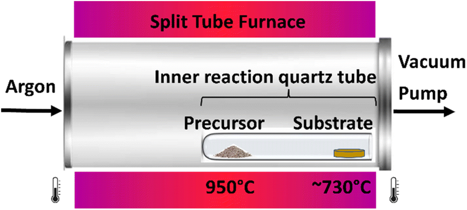 | ||
| Scheme 1 Schematic of the vapor phase transport system for ZnO nanocolumn growth. | ||
Synthesis of ZnO nanocolumns and copper doping are described in a 2-step process involving a carbothermal reduction of ZnO and CuO at 950 °C followed by catalytic crystallization by a ZnO seed layer according to the following plausible mechanism (Scheme 2):
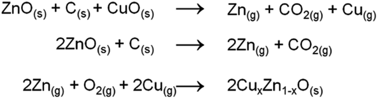 | ||
| Scheme 2 Reaction mechanism of ZnO nanocolumn synthesis and doping with Cu. | ||
Characterization methods of Cu-doped ZnO nanostructures
The morphology of the produced nanostructures was observed using scanning electron microscopy (SEM). Composition of the nanostructures was determined using energy-dispersive X-ray spectroscopy (EDS).The crystal phase of the nanostructures was identified using a Rigaku Miniflex 600 benchtop X-ray diffractometer at room temperature. The 2θ values were scanned from 20° to 65° with a current of 15 mA and a voltage of 40 kV. The crystallography database was used to identify the crystal phase of the structures.
Room temperature photoluminescence was performed using a Hitachi F-4500 Fluorescence Spectrometer. The excitation wavelength was 325 nm, and the scan was from 350 nm to 600 nm at 700 V. Slit widths were 10 nm for the excitation beam and 5 nm for the emission beam.
Results and discussion
Structural properties of undoped and Cu-doped ZnO nanostructures grown by CVD were investigated via powder XRD (Fig. 1). Signals from diffraction planes were indicative of a wurtzite crystal phase (JCPDS card no. 79-0208). High intensity of the (0 0 2) diffraction plane at 34.45° was attributed to preferred growth in the c-plane direction, which resulted in nanocolumn (NC) formation. The diffractograms show a relatively intense peak at 33.20° that represents the Si substrate and no other peaks that may represent copper metal, copper oxide, or Zn metal. This could support the idea that copper must either replace Zn atomic sites or be incorporated in the hexagonal lattice interstitially. A shift in any of the peaks cannot be seen, therefore, incorporation of copper has not changed the crystal structure. The lack of a Braggs angle shift suggests that the Cu atoms (140 pm atomic radius) have been incorporated into the crystal structure possibly replacing the Zn atoms (139 pm). As the percentage of copper increases in the sample, the relative intensity of the peaks does not change drastically. However, a decrease in crystallite size from 58 nm (undoped) to an average of 48 nm (Cu-doped) was calculated using the Debye–Scherrer equation. Such decrease in crystallite size is corroborated in the literature and may explain morphological differences between undoped and Cu-doped nanocolumns.34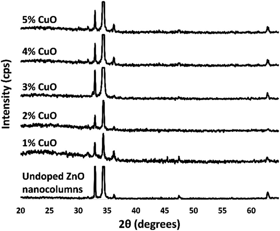 | ||
| Fig. 1 Powder X-ray diffractograms of undoped, and Cu-doped nanocolumns at different concentrations of CuO precursor. | ||
Scanning electron microscopy was utilized to investigate the morphology of the ZnO nanostructures and the influence of increasing the concentration of copper dopant on structural dimensions and shape. Scanning electron micrographs in Fig. 2 compare undoped with Cu-doped ZnO NCs.
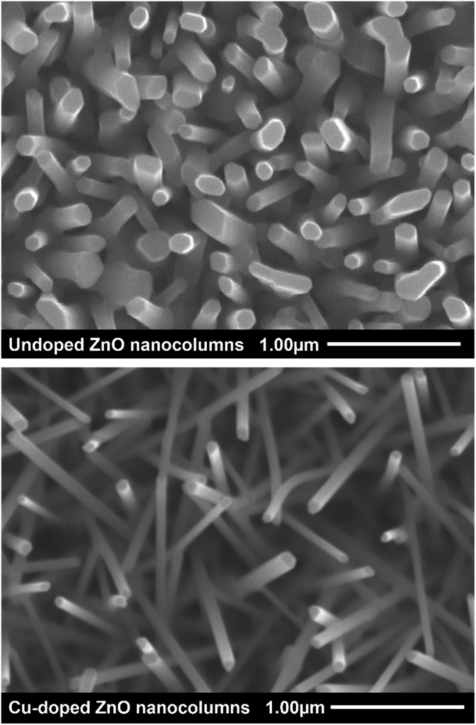 | ||
| Fig. 2 Scanning electron microscopy (SEM) images of undoped and Cu-doped ZnO nanocolumns. | ||
Morphology of both samples can be described as uniform hexagonal NCs with semi-epitaxial growth from the substrate. Uniform coverage and dispersion of NCs was achieved across the entire substrate area in this novel CVD process. The influence of copper on the diameter of the NCs is shown in Fig. 3. Average diameter, or longest cross-sectional side, of an undoped ZnO NC sample was calculated to be 135 nm. With the incorporation of copper, a drop in average diameter of Cu-doped NCs to 80 or 110 nm, depending on the concentration of dopant, occurred. Stretching of Zn–O3 and contraction of Zn–O1 bonds, where 3 and 1 correspond to the possible coordination numbers of oxygen to zinc in the wurtzite structure, is associated with sphere-to-rod shape transition and an increase in aspect ratio.35 Occupation of zinc vacancies or replacement of zinc by copper atoms on nanocolumn surface result in an overall stretching of the tri-coordinated metal center with oxygen which brings tetrahedrally bonded oxygen atoms closer to each other. The overall decrease in diameter could be attributed to a decrease in Zn–O3 bond length which has been seen by other researchers.36 Strong repulsive and weak attractive dipole moments may be created on the (0001) face of the nanocolumns due to modification in charge distribution brought by doping.37 Consequent reorientation of atomic positions would cause an increase the aspect ratio of the columns as observed in the SEM images. Nanocolumns doped with a 5% CuO precursor are noticeably smaller on average. The reason for this may be due to a saturation of oxygen in the system, which could restrict or even prevent NC growth.
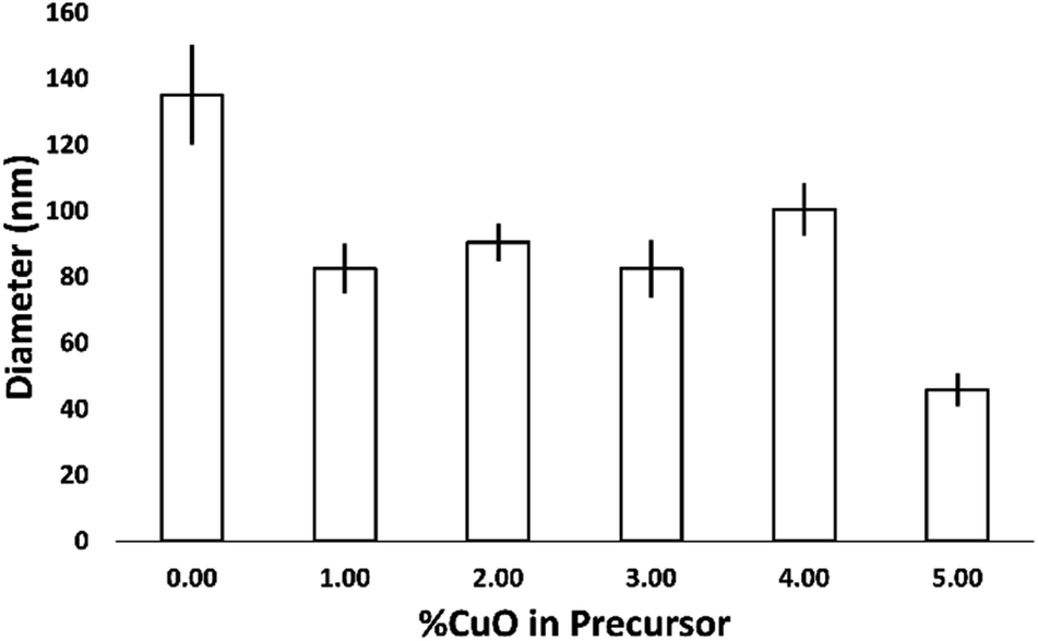 | ||
| Fig. 3 The effect of CuO concentration increase in the precursor on the diameter (or longest cross-sectional side) of ZnO NC. | ||
Energy-dispersive X-ray spectroscopy was used to understand the composition of the undoped and doped ZnO NCs (Table 1). Atomic percentages of Zn and O are close to 50% of the composition, which is indicative of the formation of ZnO. Doped copper atomic percentages in the nanowires increase linearly, 1.11–1.71%, as the amount of CuO in the starting material increases, up to 4%. When the precursor reaches 5% CuO, the ZnO crystal lattice intake of Cu seems to drop. A doping threshold around 1.7% dopant might exist for such lattice growth under aforementioned reaction conditions in the gas phase. However, it is unclear from this brief investigation whether this could be due to elevated amount of strain on the ZnO crystal structure or other factors. Most of the Cu atoms produced by carbothermal reduction will be carried across the substrate without any incorporation or interaction with the lattice on the surface. The decrease in column diameter at 5% CuO dopant suggests an inhibition of ZnO horizontal structural growth due to an interference by Cu atoms possibly kinetic in nature. One hypothesis derived from these preliminary experiments pointed at the potential of Cu incorporation at defects in the ZnO lattice. Photoluminescence studies were conducted to test this hypothesis.
| CuO% in precursor | Zn (atomic %) | O (atomic %) | Cu (atomic %) |
|---|---|---|---|
| 0 | 44.60 | 55.40 | N/A |
| 1 | 54.90 | 43.99 | 1.11 |
| 2 | 45.86 | 52.84 | 1.30 |
| 3 | 50.80 | 47.70 | 1.50 |
| 4 | 53.97 | 44.31 | 1.71 |
| 5 | 49.83 | 48.95 | 1.21 |
Photoluminescence (PL) spectra of Cu-doped ZnO and undoped NCs were evaluated in Fig. 4 to discuss certain NC structural and optical aspects. A typical peak in the green region of 496 nm for the undoped nanowires and the doped samples that used a CuO precursor at 1%, 2%, 3%, 4%, and 5% have peaks in the 482–501 nm range. The origin of this peak comes from oxygen vacancies and other defects, which are common with ZnO nanostructures. A less defined peak is present in the UV region at 389 nm for the undoped NCs and 396 nm for the Cu-doped NCs. Decrease in the intensity of this near-band emission (NBE) peak for the Cu-doped nanowires is evidence of a longer e−–h+ lifetime.38 A noticeable decrease is apparent in this NBE peak for all of the Cu-doped nanowires supporting the argument of reduced rate of recombination, but also corroborating a decrease in crystalline quality with Cu doping due to interference with the wurtzite phase formation.25,34 Nevertheless, as doping increases, enhancement in carrier concentration and mobility is predicted in the conduction band of the semiconductor.39,40 Similar observation was noted in ZnO films doped with Cu at concentrations analogous to those presented here, where crystallinity was suggested to improve along the ZnO (002) plane up to 3% concentration of Cu.41 Surprisingly, further increase in Cu doping (5%) lead to a drop in crystallinity possibly due to high compressive strain.42 Furthermore, studies using a structure zone model for polycrystalline metallic films attributed shrinkage of crystallite sizes to impurity segregation at film grain boundaries as the impurity content increased.42 This could support a threshold at optimum concentration of 4% Cu doping for the best quality Cu-doped nanocolumns. The lack of resolution of the NBE peak is due to additional defects that appear from this particular CVD method. Vempati and colleagues compiled the various ZnO defects and their transition wavelengths.43 Specifically, two defects are most likely being expressed here. The Zni to VZn transition produces a signal at 395 nm in room temperature photoluminescence and the conduction band to VZn transition produces a signal at 405 nm.36,44,45 Redshift of the NBE peak is a reduction of the bandgap (3.18–3.13 eV) from the doping of Cu.46
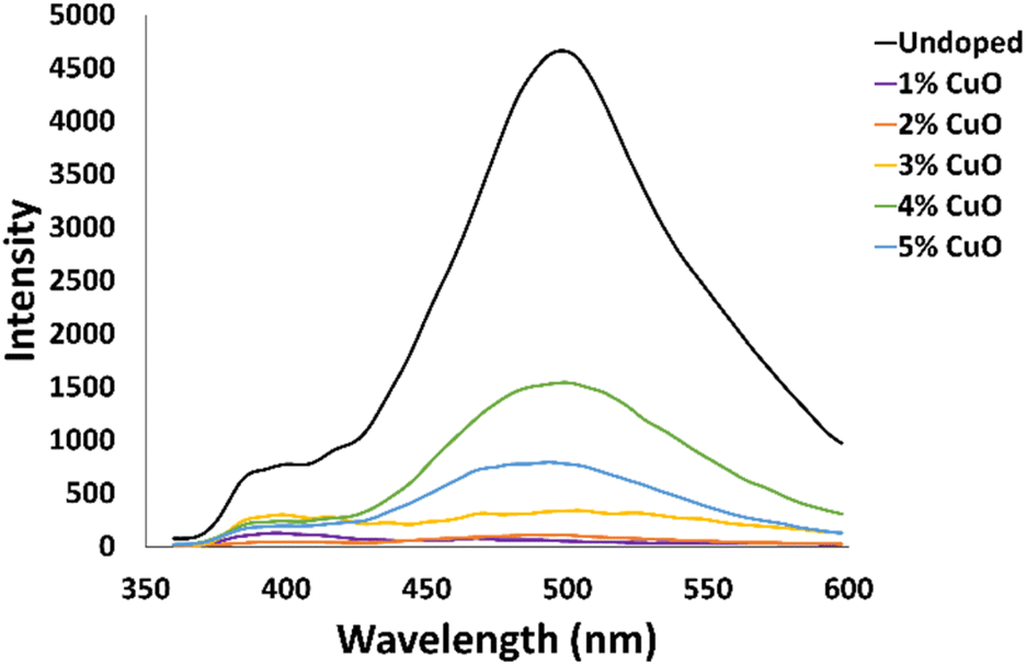 | ||
| Fig. 4 Photoluminescence spectra of undoped ZnO (black line) and Cu-doped ZnO NCs with different CuO concentrations in the precursor (other colors). | ||
Interesting similarities can be drawn from N-doped ZnO, a stable p-type semiconductor. Nitrogen replaces oxygen (rather than Zn in the case of Cu-doped ZnO) leading to a surplus of holes in the system without placing strain on the structure.19 Doping ZnO with nitrogen also leads to a reduced band gap which is consistent with typical p-type doping and Cu-doped ZnO.47 Cu behaves as an acceptor in ZnO with its energy level located at 0.17 eV below the conduction band which makes it a good candidate for promoting p-type conduction in ZnO.48 Sb-doped ZnO on the other hand has a significant difference in its structure. Unlike N-doped and Cu-doped ZnO, Sb is incorporated into the lattice much differently. Instead of replacing a Zn or O atom directly, it is incorporated interstitially.49 Due to its size and electron configuration, two VZn are formed leading to a shift in the crystal structure.49 Therefore, p-type nature of Sb-ZnO could be a result of an excess of holes acting as the electron-poor species in available Zn vacancies. The structural strain from the antimony can also lead to an increase in the size of the crystal structure, which isn't observed in Cu-doped ZnO.50 Understanding doping effects on the properties of useful and common semiconducting nanostructures allows for tailored synthesis of promising components in future green-optoelectronic devices.
Conclusions
Cu-doped ZnO NCs were synthesized using a novel CVD method. Utilization of concentrated Zn atmosphere within an inner reaction tube resulted in uniform growth and large substrate coverage. Upon dopant introduction in the ZnO crystal lattice, NC average diameter dropped from 135 nm to under 100 nm. Photoluminescence data shows that the undoped ZnO nanocolumns have additional defects that are atypical in most ZnO nanostructures. The expression of these defects may suggest p-type conductivity not only in the doped structures but in the undoped nanostructures as well. The addition of Cu shows a decrease in the optical band gap by 0.05 eV and a consequential increase in electron–hole (e−–h+) lifetime, suggesting reduced e−–h+ recombination rate. Cu-doped ZnO NC properties realized in this work show potential towards PCE increase in ZnO-based p-type DSSCs. Incorporation of the doped NCs in DSSCs and PCE investigations are currently underway and will be reported in a complimentary article.Author contributions
The manuscript was written with equal contributions from all authors. All authors have given approval of the final version of the manuscript.Conflicts of interest
There are no conflicts to declare.Acknowledgements
The authors would like to thank Dr Brian Cooper and the environmental and geosciences department at SHSU for facilitating access to powder X-ray diffraction. Acknowledgments are also due to Dr Aniruddha Acharya for his help with electron microscopy and EDS. This work was funded partially by the Welch Foundation Departmental grant (# X-0011).Notes and references
- A. Hagfeldt, G. Boschloo, L. Sun, L. Kloo and H. Pettersson, Chem. Rev., 2010, 110, 6595–6663 CrossRef PubMed.
- A. Yella, H.-W. Lee, H. N. Tsao, C. Yi, A. K. Chandiran, M. K. Nazeeruddin, E. W.-G. Diau, C.-Y. Yeh, S. M. Zakeeruddin and M. Grätzel, Science, 2011, 334, 629 CrossRef PubMed.
- M. Grätzel, Acc. Chem. Res., 2009, 42, 1788–1798 CrossRef PubMed.
- C.-P. Lee, C.-T. Li and K.-C. Ho, Mater. Today, 2017, 20, 267–283 CrossRef.
- W. S. Yang, J. H. Noh, N. J. Jeon, Y. C. Kim, S. Ryu, J. Seo and S. I. Seok, Science, 2015, 348, 1234 CrossRef CAS.
- M. Grätzel, Inorg. Chem., 2005, 44, 6841–6851 CrossRef.
- J. Yu, Y. Yang, R. Fan, D. Liu, L. Wei, S. Chen, L. Li, B. Yang and W. Cao, Inorg. Chem., 2014, 53, 8045–8053 CrossRef CAS.
- W. Shao, F. Gu, C. Li and M. Lu, Inorg. Chem., 2010, 49, 5453–5459 CrossRef CAS PubMed.
- J. A. Anta, E. Guillén and R. Tena-Zaera, J. Phys. Chem. C, 2012, 116, 11413–11425 CrossRef CAS.
- H. Horiuchi, R. Katoh, K. Hara, M. Yanagida, S. Murata, H. Arakawa and M. Tachiya, J. Phys. Chem. B, 2003, 107, 2570–2574 CrossRef CAS.
- L.-C. Chen, Y.-J. Tu, Y.-S. Wang, R.-S. Kan and C.-M. Huang, J. Photochem. Photobiol., A, 2008, 199, 170–178 CrossRef CAS.
- F. Odobel, L. Le Pleux, Y. Pellegrin and E. Blart, Acc. Chem. Res., 2010, 43, 1063–1071 CrossRef.
- S. D. Chavhan, R. D. Abellon, A. J. J. M. van Breemen, M. M. Koetse, J. Sweelssen and T. J. Savenije, J. Phys. Chem. C, 2010, 114, 19496–19502 CrossRef.
- C. H. Park, S. B. Zhang and S.-H. Wei, Phys. Rev. B: Condens. Matter Mater. Phys., 2002, 66, 073202 CrossRef.
- D. C. Look, R. L. Jones, J. R. Sizelove, N. Y. Garces, N. C. Giles and L. E. Halliburton, Phys. Status Solidi A, 2003, 195, 171–177 CrossRef.
- Y. R. Ryu, S. Zhu, D. C. Look, J. M. Wrobel, H. M. Jeong and H. W. White, J. Cryst. Growth, 2000, 216, 330–334 CrossRef.
- D. C. Look and B. Claflin, Phys. Status Solidi B, 2004, 241, 624–630 CrossRef.
- S. Limpijumnong, S. B. Zhang, S.-H. Wei and C. H. Park, Phys. Rev. Lett., 2004, 92, 155504 CrossRef PubMed.
- B. Chavillon, L. Cario, A. Renaud, F. Tessier, F. Cheviré, M. Boujtita, Y. Pellegrin, E. Blart, A. Smeigh, L. Hammarström, F. Odobel and S. Jobic, J. Am. Chem. Soc., 2012, 134, 464–470 CrossRef PubMed.
- Y. Yang, K. C. Pradel, Q. Jing, J. M. Wu, F. Zhang, Y. Zhou, Y. Zhang and Z. L. Wang, ACS Nano, 2012, 6, 6984–6989 CrossRef.
- C. J. Raj, K. Prabakar, S. N. Karthick, K. V. Hemalatha, M.-K. Son and H.-J. Kim, J. Phys. Chem. C, 2013, 117, 2600–2607 CrossRef.
- G. Kanimozhi, S. Vinoth, H. Kumar, E. S. Srinadhu and N. Satyanarayana, J. Electron. Mater., 2019, 48, 4389–4399 CrossRef.
- M. Mohamed, A. Sedky, A. S. Alshammari and M. Gandouzi, J. Mater. Sci.: Mater. Electron., 2021, 32, 5186–5198 CrossRef.
- B. Mehmood, M. I. Khan, M. Iqbal, A. Mahmood and W. Al-Masry, Int. J. Energy Res., 2021, 45, 2445–2459 CrossRef.
- F. Ghahramanifard, A. Rouhollahi and O. Fazlolahzadeh, Superlattices Microstruct., 2018, 114, 1–14 CrossRef.
- Z. Ge, C. Wang, T. Chen, Z. Chen, T. Wang, L. Guo, G. Qi and J. Liu, J. Phys. Chem. Solids, 2021, 150, 109833 CrossRef.
- P. Abbasi and V. Dalouji, Indian J. Phys., 2021, 95, 1741–1750 CrossRef.
- S. Zhuang, M. Lu, N. Zhou, L. Zhou, D. Lin, Z. Peng and Q. Wu, Electrochim. Acta, 2019, 294, 28–37 CrossRef.
- L. C.-K. Liau and J.-S. Huang, J. Alloys Compd., 2017, 702, 153–160 CrossRef.
- N. M. Alatawi, L. B. Saad, L. Soltane, A. Moulahi, I. Mjejri and F. Sediri, Polyhedron, 2021, 197, 115022 CrossRef.
- M. Ristić, S. Musić, M. Ivanda and S. Popović, J. Alloys Compd., 2005, 397, L1–L4 CrossRef.
- M. Saini, R. Singh, A. Mitra and T. Som, Sol. Energy, 2020, 207, 228–234 CrossRef.
- R. Müller, F. Huber, M. Töws, M. Mangold, M. Madel, J.-P. Scholz, A. Minkow, U. Herr and K. Thonke, Cryst. Growth Des., 2020, 20, 3918–3926 CrossRef.
- R. Bhardwaj, A. Bharti, J. P. Singh, K. H. Chae and N. Goyal, Nanoscale Adv., 2020, 2, 4450–4463 RSC.
- M. Ghosh, D. Karmakar, S. Basu, S. N. Jha, D. Bhattacharyya, S. C. Gadkari and S. K. Gupta, J. Phys. Chem. Solids, 2014, 75, 543–549 CrossRef.
- C. H. Ahn, Y. Y. Kim, D. C. Kim, S. K. Mohanta and H. K. Cho, J. Appl. Phys., 2009, 105, 013502 CrossRef.
- S. Dag, S. Wang and L.-W. Wang, Nano Lett., 2011, 11, 2348–2352 CrossRef PubMed.
- C.-C. Wang, W.-C. Lin, F.-S. Shieu and H. C. Shih, AIP Adv., 2019, 9, 125019 CrossRef.
- S.-H. Lee, S.-H. Han, H. S. Jung, H. Shin, J. Lee, J.-H. Noh, S. Lee, I.-S. Cho, J.-K. Lee, J. Kim and H. Shin, J. Phys. Chem. C, 2010, 114, 7185–7189 CrossRef.
- T. S. Herng, S. P. Lau, S. F. Yu, H. Y. Yang, L. Wang, M. Tanemura and J. S. Chen, Appl. Phys. Lett., 2007, 90, 032509 CrossRef.
- E. M. Mkawi, K. Ibrahim, M. K. M. Ali, M. A. Farrukh and A. S. Mohamed, Appl. Nanosci., 2015, 5, 993–1001 CrossRef.
- R. D. Shannon, Acta Crystallogr., Sect. A: Cryst. Phys., Diffr., Theor. Gen. Crystallogr., 1976, 32, 751–767 CrossRef.
- S. Vempati, J. Mitra and P. Dawson, Nanoscale Res. Lett., 2012, 7, 470 CrossRef.
- E. G. Bylander, J. Appl. Phys., 1978, 49, 1188–1195 CrossRef.
- B. Lin, Z. Fu and Y. Jia, Appl. Phys. Lett., 2001, 79, 943–945 CrossRef CAS.
- A. M. El Sayed, G. Said, S. Taha, A. Ibrahim and F. Yakuphanoglu, Superlattices Microstruct., 2013, 62, 47–58 CrossRef CAS.
- X. Zong, C. Sun, H. Yu, Z. G. Chen, Z. Xing, D. Ye, G. Q. Lu, X. Li and L. Wang, J. Phys. Chem. C, 2013, 117, 4937–4942 CrossRef CAS.
- Z. Zhang, J. B. Yi, J. Ding, L. M. Wong, H. L. Seng, S. J. Wang, J. G. Tao, G. P. Li, G. Z. Xing, T. C. Sum, C. H. Alfred Huan and T. Wu, J. Phys. Chem. C, 2008, 112, 9579–9585 CrossRef.
- C. Luo, L.-P. Ho, F. Azad, W. Anwand, M. Butterling, A. Wagner, A. Kuznetsov, H. Zhu, S. Su and F. C.-C. Ling, J. Appl. Phys., 2018, 123, 161525 CrossRef.
- A. M. Alsmadi, B. Salameh, L. L. Kerr and K. F. Eid, Phys. B, 2018, 545, 519–526 CrossRef.
| This journal is © The Royal Society of Chemistry 2022 |