
 Open Access Article
 This Open Access Article is licensed under a Creative Commons Attribution-Non Commercial 3.0 Unported Licence
Improving the efficiency of n-Si/PEDOT:PSS hybrid solar cells by incorporating AuNP-decorated graphene oxide as a nanoadditive for conductive polymers
Nguyen Van Tua,
Nguyen Ngoc Anha,
Tran Van Hau a,
Nguyen Van Haoc,
Nguyen Thi Huyena,
Bui Hung Thanga,
Phan Ngoc Minhab,
Nguyen Van Chuc*a,
Naoki Fukatad and
Pham Van Trinh*ab
a,
Nguyen Van Haoc,
Nguyen Thi Huyena,
Bui Hung Thanga,
Phan Ngoc Minhab,
Nguyen Van Chuc*a,
Naoki Fukatad and
Pham Van Trinh*ab
aInstitute of Materials Science, Vietnam Academy of Science and Technology, 18 Hoang Quoc Viet Str., Cau Giay Distr., Hanoi, Vietnam. E-mail: trinhpv@ims.vast.vn; chucnv@ims.vast.vn; Tel: +84 94 319 0301
bGraduate University of Science and Technology, Vietnam Academy of Science and Technology, 18 Hoang Quoc Viet, Hanoi, Vietnam
cInstitute of Science and Technology, TNU-University of Science, Tan Thinh Ward, Thai Nguyen City, Vietnam
dInternational Center for Materials Nanoarchitectonics, National Institute for Materials Science, 1-1 Namiki, Tsukuba, Ibaraki 305-0044, Japan
First published on 28th September 2022
Abstract
A gold nanoparticle-decorated graphene oxide (GO-AuNP) hybrid material was prepared by using the chemical reduction method. The obtained results showed that the AuNPs of about of 15 nm are well bound on the surface of GO. The GO-AuNP hybrid material was used for transparent conductive film (TCF) and organic/inorganic hybrid solar cells. The TCF based on poly(3,4-ethylenedioxythiophene):poly(styrene sulfonate) (PEDOT:PSS) containing GO-AuNPs was fabricated at room temperature. The obtained results show that the TCF containing 0.5 wt% GO-AuNPs has a high transmittance of 69.7% at 550 nm, a low sheet resistance of 50.5 Ω □−1 and a conductivity that increased to 3960 S cm−1, which is three times higher than those of the PEDOT:PSS and PEDOT:PSS/GO film. The power conversion efficiency (PCE) of the n-Si/PEDOT:PSS hybrid solar cell containing GO-AuNPs was 8.39% and is higher than pristine PEDOT:PSS (5.81%) and PEDOT:PSS/GO (7.58%). This is a result of the increased electrical conductivity and localized surface plasmon resonance of the PEDOT:PSS coating layer containing the GO-AuNP hybrid material.
1. Introduction
Graphene is a new nanostructured material with superior mechanical, thermal and electrical properties such as high thermal conductivity 5000 W m−1 K−1, extremely high surface area 2630 m2 g−1, high Young's modulus of about 1 TPa and high electron mobility of 200![[thin space (1/6-em)]](https://www.rsc.org/images/entities/char_2009.gif) 000 cm2 V−1 s−1.1–4 All these remarkable properties make graphene a rising star in many fields of application such as in the electronics industry as electronics devices, superconductors, electrochemical sensors, etc.5–11 However, the nature of graphene also has certain disadvantages such as being easily clumped together by van der Waals forces and π–π interactions.12,13 In fact, graphene or graphene oxide often has structural defects during fabrication such as fractures, and functional groups attached to the surface of the graphene material. Such structural defects lead to the deterioration of the superior properties of graphene such as reduced conductivity, reduced electrochemical and photoelectric properties, etc.14–17 To solve the above problem, recently, hybrid materials between graphene and metal nanoparticles or metal oxides has been prepared.18–27 The presence of metal nanoparticles located at the defect point are expected to improve the conductivity of the material properties significantly.28–30 Hybrid materials have outstanding advantages in terms of thermal and electrical properties that can be applied in different fields such as sensors, composites, opto-electronic components.19,21,22,25,29 In some cases, these hybrid materials not only transcend the restrictions of employing a single component, but they also give a higher surface area, particularly excellent catalytic capabilities, higher specificity, etc.24,25,27 In addition, the addition of metal nanoparticles between the graphene layers can minimize the agglomeration due to the π–π interaction between the graphene layers.31,32 Besides, the presence of metal nanoparticles such as AuNPs or AgNPs as light-capturing plasmonic layer is expected to improve the photoelectric properties of graphene in optoelectronic devices.28,33–39 From the foregoing results, it is clear that further research on the characteristics of GO-AuNPs hybrid materials is needed for possible applications in optoelectronic devices, sensors, etc. …
000 cm2 V−1 s−1.1–4 All these remarkable properties make graphene a rising star in many fields of application such as in the electronics industry as electronics devices, superconductors, electrochemical sensors, etc.5–11 However, the nature of graphene also has certain disadvantages such as being easily clumped together by van der Waals forces and π–π interactions.12,13 In fact, graphene or graphene oxide often has structural defects during fabrication such as fractures, and functional groups attached to the surface of the graphene material. Such structural defects lead to the deterioration of the superior properties of graphene such as reduced conductivity, reduced electrochemical and photoelectric properties, etc.14–17 To solve the above problem, recently, hybrid materials between graphene and metal nanoparticles or metal oxides has been prepared.18–27 The presence of metal nanoparticles located at the defect point are expected to improve the conductivity of the material properties significantly.28–30 Hybrid materials have outstanding advantages in terms of thermal and electrical properties that can be applied in different fields such as sensors, composites, opto-electronic components.19,21,22,25,29 In some cases, these hybrid materials not only transcend the restrictions of employing a single component, but they also give a higher surface area, particularly excellent catalytic capabilities, higher specificity, etc.24,25,27 In addition, the addition of metal nanoparticles between the graphene layers can minimize the agglomeration due to the π–π interaction between the graphene layers.31,32 Besides, the presence of metal nanoparticles such as AuNPs or AgNPs as light-capturing plasmonic layer is expected to improve the photoelectric properties of graphene in optoelectronic devices.28,33–39 From the foregoing results, it is clear that further research on the characteristics of GO-AuNPs hybrid materials is needed for possible applications in optoelectronic devices, sensors, etc. …
Thus, the goal of this work is to prepare the GO-AuNP hybrid material for enhancing the performance of the transparent conductive film and organic/inorganic hybrid solar cells. The GO-AuNP hybrid materials with AuNPs having an average size of 15 nm in diameter were prepared by using the chemical reduction method. The microstructure of GO-AuNP hybrid material was investigated. The effects of the GO-AuNPs hybrid material on the properties of transparent conductive thin film and the hybrid solar cells were also investigated.
2. Experimental
2.1. Preparation of AuNPs decorated GO
The GO-AuNPs hybrid material was prepared by the chemical reduction process. First, 100 ml of a 0.2 mM solution of chloroauric acid (HAuCl4·3H2O, Sigma Aldrich) was introduced to a 500 ml beaker of GO-containing solution (0.1 g l−1) under continuous magnetic stirring. Consequently, a sodium borohydride solution (NaBH4, Sigma Aldrich) 0.1 M was slowly added to the solution containing HAuCl4 and GO under constant stirring. The stirring process was continued for 10 minutes to obtain a homogenous solution. Afterwards, the above solution was filtered and washed with distilled water to obtain GO-AuNP hybrid material. Finally, the hybrid materials were disseminated in deionized water by ultrasonication for 45 minutes and then kept in the dark to reduce oxidation.2.2. Preparation of PEDOT:PSS/GO-AuNPs thin films
The PEDOT:PSS/GO-AuNPs transparent conductive film was prepared by the following steps: firstly, GO-AuNPs solution with a concentration 1 mg/1 ml of was put into PEDOT:PSS with a fixed concentrations of 0.5 wt% and then stirred for 6 hours to uniformly disperse GO-AuNPs in the PEDOT:PSS. Secondly, the mixture of PEDOT:PSS/GO-AuNPs is coated on the glass substrate by spin coating method with the condition of 10 seconds (2000 rpm) and followed up 60 seconds (6000 rpm). Finally, the prepared film was annealed at 140 °C for 30 minutes with the heating and cooling speed of 2 °C per min in a N2 environment to create thin film structure.2.3. Preparation of n-Si/PEDOT:PSS/GO-AuNPs hybrid solar cell
The manufacturing process of the solar cells based on n-Si/PEDOT:PSS/GO-AuNPs hybrid structure is illustrated in Fig. 1. The n-Si substrate was firstly treated with a solution of piranha at 130 °C for 40 min to remove organic compound on the surface. After that, the treated Si substrate was cleaned in turn with acetone, alcohol and deionized water for several times at room temperature. The n-Si substrate was then processed in a 2% HF solution for two minutes to strip off SiO2 formed on the surface. Immediately, the PEDOT:PSS/GO-AuNPs compound was coated on the n-Si substrate by using the spin coating at condition of 2000 rpm for 10 s and followed up 6000 rpm for 60 s. The obtained structure was then annealed in N2 atmosphere at 140 °C for 30 min to remove residual water. Finally, the front and back electrodes were fabricated by using the sputtering technique. In which, the finger-typed electrode deposited on the top of the structure is made of Ag with a thickness of 200 nm, and the rear electrode is made of Ti (50 nm)/Ag (200 nm). The hybrid solar cells with only PEDOT:PSS and PEDOT:PSS/GO are also prepared with the same conditions for comparison.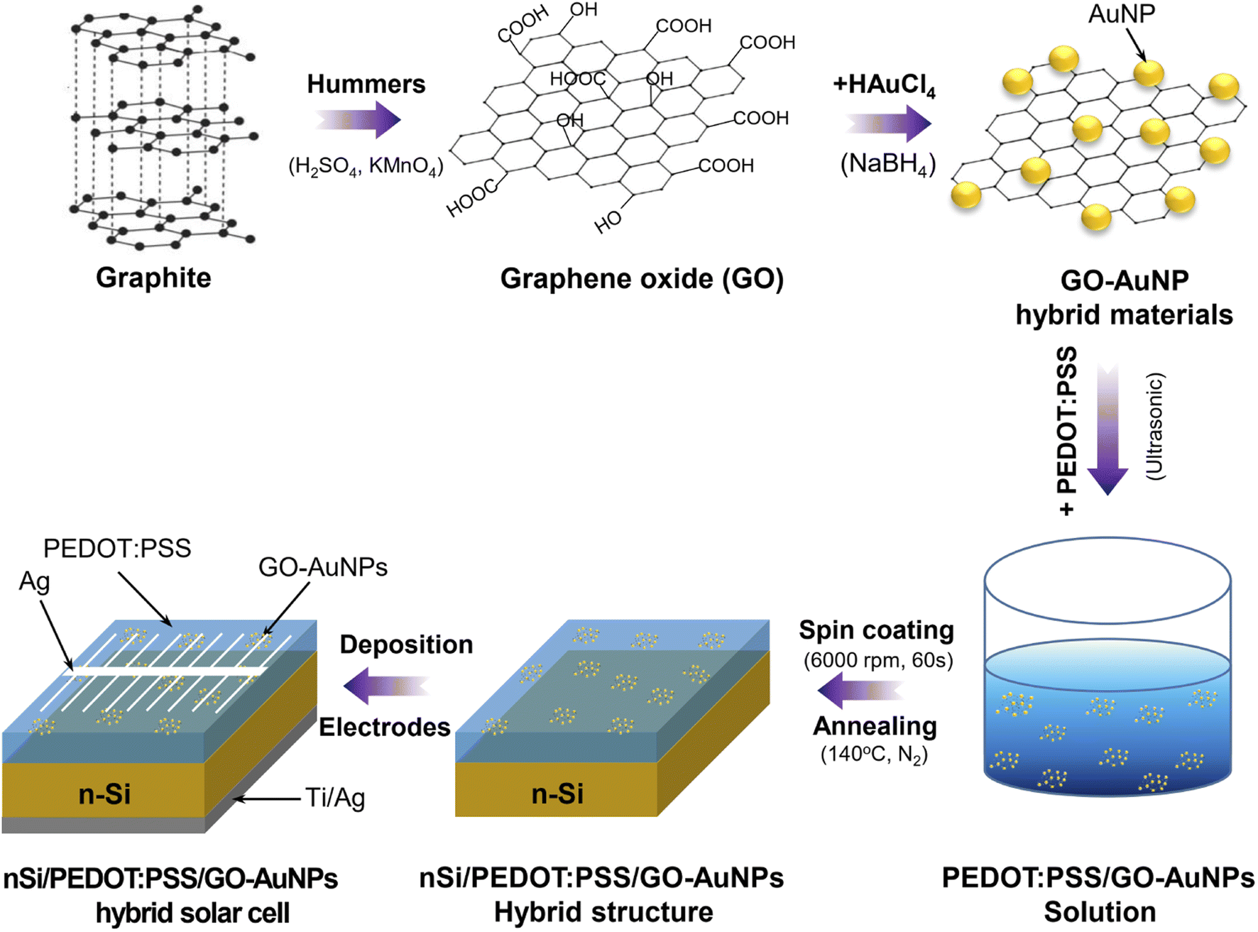 | ||
| Fig. 1 Schematic view of the preparation process of n-Si/PEDOT:PSS/GO-AuNPs hybrid solar cells. | ||
2.4. Characterization
The morphology of the samples was analyzed using SEM (Hitachi S4800) and HRTEM (Jeon-JEM 2100). A JASCO V-770 spectrophotometer was used to measure the absorption spectra. The XRD pattern was measured by using a XRD Bruker D8 Endeavor equipped with CuKα radiation. The Raman spectra of samples were recorded by using XploRA, Horiba Jobin-Yvon spectroscopy. The NPS Sigma-5+ based on 4-point technique were used to measure the sheet resistance of the PEDOT:PSS/GO-AuNPs thin film. The PCE of the hybrid solar cells was measured with a Keithley 2400 source meter under AM 1.5 G with 100 mW cm−2 illumination.3. Results and discussions
Fig. 2a shows the FESEM image of GO with an average thickness estimated to be few nanometers prepared by using the Hummers' method. Fig. 2b shows the FESEM images of GO-AuNPs hybrid materials, in which GO with AuNPs attached by chemical reduction method. Fig. 2c is a TEM image of the hybrid material sample. From the TEM image, as can be seen that AuNPs are tightly attached to the graphene sheets. Statistical analysis showed that the average size of AuNPs in the hybrid material was about 15 nm (Fig. 2d). Most of the particles were of medium size, but a few particles > 20 nm were also found in the sample. The average size distribution of AuNPs depends on the solvent medium and also on the GO content in the solution. This issue will be studied in the following sections.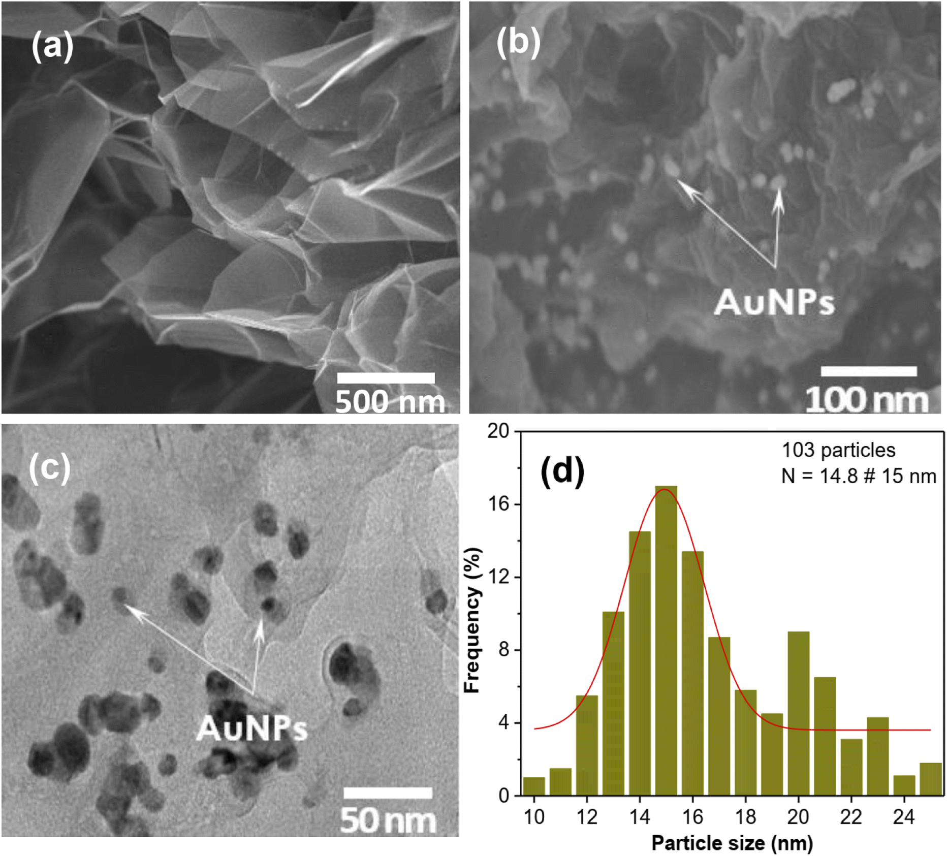 | ||
| Fig. 2 SEM images of GO (a) and GO-AuNPs (b); TEM image of GO-AuNPs (c) and size distribution of AuNPs (d). | ||
UV-vis spectroscopy was used to validate the formation of GO-AuNPs hybrid material. The UV-vis spectra of GO and GO-AuNPs is presented in Fig. 3a. The UV-vis spectra of GO exhibit two peaks at 249 and 344 nm. This is attributed to the π → π* aromatic C–C and C![[double bond, length as m-dash]](https://www.rsc.org/images/entities/char_e001.gif) C phase transition.40 Two peaks with a red shift can be seen in the UV-vis spectra of GO-AuNPs. These peaks are attributable to the aromatic C–C transition of GO and the surface plasmon resonance of AuNPs, respectively.41,42 These results provide more evidence that GO-AuNPs hybrid materials were formed. Fig. 3b shows Raman scattering confirming the transition between GO and GO-AuNPs. Raman spectra of GO exhibits D and G peaks at 1350 cm−1 and 1579 cm−1, respectively. The intensity ratio between D and G peaks (ID/IG) of GO-AuNPs (1.05) is higher than that of GO (0.68), which indicates that the appearance of AuNPs on the surface of GO causes some lattice defects in terms of structure compared to the original. Fig. 3c shows the XRD pattern of GO, and GO-AuNPs. The XRD of GO shows a typical peak at 2θ = 10.90°, indicated that the graphite has been completely separated into graphene sheets. XRD of the GO-AuNPs hybrid material shows some typical peaks at 38.20°, 44.30° and 65.20° corresponding to the (111), (200) and (220) planes, respectively which are assigned to the Au-centered cubic plane. The obtained results confirmed that Au(I) was completely converted to Au(0). The average diameter of AuNPs of about 15.2 nm was calculated using the Scherer equation. This result is reasonably accurate compared to the data obtained from SEM and TEM measurements. Thus, the XRD results demonstrated that AuNPs were successfully attached on the surface of GO sheets to form GO-AuNPs hybrid material.
C phase transition.40 Two peaks with a red shift can be seen in the UV-vis spectra of GO-AuNPs. These peaks are attributable to the aromatic C–C transition of GO and the surface plasmon resonance of AuNPs, respectively.41,42 These results provide more evidence that GO-AuNPs hybrid materials were formed. Fig. 3b shows Raman scattering confirming the transition between GO and GO-AuNPs. Raman spectra of GO exhibits D and G peaks at 1350 cm−1 and 1579 cm−1, respectively. The intensity ratio between D and G peaks (ID/IG) of GO-AuNPs (1.05) is higher than that of GO (0.68), which indicates that the appearance of AuNPs on the surface of GO causes some lattice defects in terms of structure compared to the original. Fig. 3c shows the XRD pattern of GO, and GO-AuNPs. The XRD of GO shows a typical peak at 2θ = 10.90°, indicated that the graphite has been completely separated into graphene sheets. XRD of the GO-AuNPs hybrid material shows some typical peaks at 38.20°, 44.30° and 65.20° corresponding to the (111), (200) and (220) planes, respectively which are assigned to the Au-centered cubic plane. The obtained results confirmed that Au(I) was completely converted to Au(0). The average diameter of AuNPs of about 15.2 nm was calculated using the Scherer equation. This result is reasonably accurate compared to the data obtained from SEM and TEM measurements. Thus, the XRD results demonstrated that AuNPs were successfully attached on the surface of GO sheets to form GO-AuNPs hybrid material.
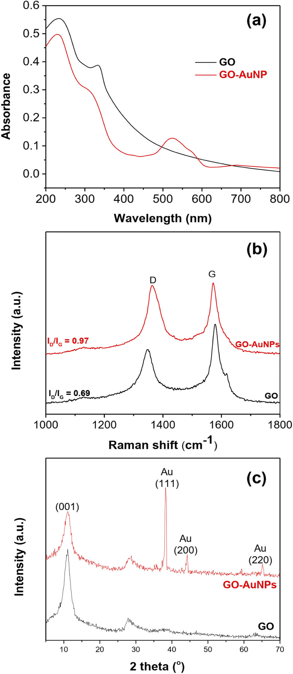 | ||
| Fig. 3 (a) Optical absorption spectra, (b) Raman spectra and (c) XRD pattern of GO and GO-AuNPs. | ||
The optical and electrical properties of the PEDOT:PSS/GO-AuNPs compound were investigated in order to determine the impact that the GO-AuNPs hybrid material had on these characteristics. Fig. 4a shows the SEM image of the PEDOT:PSS/GO-AuNPs conductive thin film on a glass substrate. As observed, the thickness of the film was measure about 50 nm. The transmittance of PEDOT:PSS/GO-AuNPs film is shown in Fig. 4b. It can be found that when compared with thin films containing only GO, the transmittance of films containing GO-AuNPs is lower. The transmittance at 550 nm was determined to be 86.6%, 71.6% and 69.7% for the PEDOT:PSS, PEDOT:PSS/GO and PEDOT:PSS/GO-AuNPs thin films, respectively. Surface resistance of the PEDOT:PSS, PEDOT:PSS/GO and PEDOT:PSS/GO-AuNPs thin films are shown in Fig. 4c. The sheet resistance values were measured to be 249.6, 150.7 and 50.5 Ω Ω−1 corresponding to PEDOT:PSS, PEDOT:PSS/GO and PEDOT:PSS/GO-AuNPs thin film, respectively. As a result, the incorporation of the GO resulted in a reduction in the sheet resistance of the PEDOT:PSS thin film. Notably, when using the hybrid GO-AuNPs material, the surface resistance is significantly reduced. The decrease in the sheet resistance for thin films containing GO-AuNPs hybrid materials was attributed to be the presence of good conductive AuNPs attached to the functional group sites on the surface of the graphene sheets.
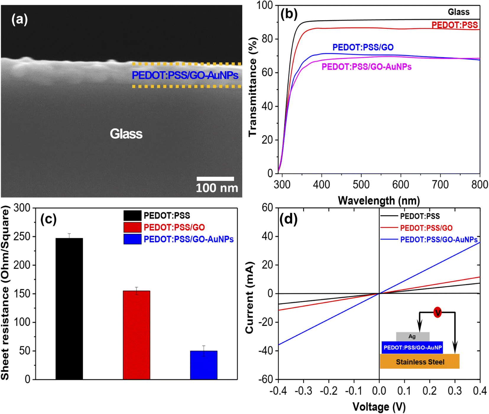 | ||
| Fig. 4 (a) SEM image of conductive thin film PEDOT:PSS/GO-AuNPs, (b) transmittance, (c) surface resistance and (d) current–voltage (I–V) characterization of PEDOT:PSS, PEDOT:PSS/GO and PEDOT:PSS/GO-AuNPs films. | ||
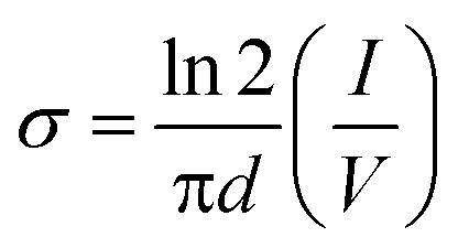
I–V characteristic measurement is used to accurately evaluate the electrical properties of thin films. The thin film is fabricated on a glass substrate and all electrode connections are made with the help of gold wire. Gold wires are mounted on thin film at four corners with silver glue. All connections are made out according to the Van der Pauw four-probe method.43 The in-plane conductivity of the films was estimated using the following eqn (1):44
 | (1) |
Characteristics of n-Si/PEDOT:PSS/GO-AuNP hybrid solar cells, including energy diagram and current–voltage (J–V) curves, are shown in Fig. 5. In this configuration, n-type Si served as both the light-absorbing layer and the electron–hole pair generator. The PEDOT:PSS layer functions as a p-type semiconductor material as well as a hole transport layer. The separation of electron–hole pairs takes place at the Si/PEDOT:PSS interfaces (Fig. 5a). The properties of the n-Si/PEDOT:PSS hybrid solar cells with different compositions are shown in Fig. 5b and Table 1. From the J–V characteristics, the n-Si/PEDOT:PSS hybrid solar cells without GO, the achieved PCE is 5.81% with a short circuit current density (JSC) of 25.01 mA.cm−2, an open circuit voltage (VOC) of 0.484 V and a fill factor (FF) of 48%. When the GO component is added, the efficiency of the devices increases to 7.58%. The hybrid solar cell containing GO-AuNPs showed the highest PCE of 8.39% with a JSC of 26.23 mA.cm−2 VOC of 0.525 V and an FF factor of 61%, which are higher than those of the solar cell with PEDOT:PSS only. The obtained results are consistent with previous reports.45–48 According to Lu et al., the PCE of a SiNHs/PEDOT:PSS hybrid solar cell including AuNPs was 6.1%, which is a 27% improvement over the solar cells without AuNPs.45 Similarly, Sharma et al. found an 8.2% PCE for planar Si/PEDOT:PSS/AuNPs, which is greater than the device without AuNPs (7.3%).46,47 Kim and colleagues reported a higher PCE for Si/PEDOT:PSS/AuNPs hybrid solar cells, with an in situ method measuring a PCE of 11.19% for the device containing AuNPs, roughly 19% higher than the device without AuNPs (9.42%).48 Incorporating carbon nanomaterials into PEDOT:PSS allowed Uma et al. to achieve a PCE of 9.57% in hybrid solar cell containing GO. However, it is important to note that this structure required the use of silicon nanowires (SiNW) as substrate to improve the light absorption.49 The increased PCE of solar cells with the addition of GO-AuNPs could be attributed to the increase of the conductivity of the PEDOT:PSS/GO-AuNPs compound. Besides, there is a possibility that the AuNPs served as antennae for the incident light, leading to the improvement. Energy could be stored in a confined surface plasmon mode using these antennas.50,51 The trend of increasing and decreasing the conversion efficiency of solar cells is almost similar to the increase and decrease of conductivity of PEDOT:PSS/GO-AuNPs films. Furthermore, the presence of AuNPs in the hybrid solar cell will improve the optical absorption of the PEDOT:PSS/AuNPs resulted from the light-trapping effect of AuNPs at wavelengths below 500 nm. Consequently, the external quantum efficiency (EQE) of the hybrid solar cell will be enhanced in the wavelength range from 300 to 600 nm as addressed in the previous work.50,51 The dark J–V characteristic curve of the solar cell is shown in Fig. 5c. The obtained results show that GO-AuNPs hybrid materials have an effect on the properties of the hybrid solar cells. As a result, the devices that included GO-AuNPs exhibited the lowest current density. The obtained results exhibited that the decrease in the leakage current is much improved in comparison to the solar cell containing GO or pristine PEDOT:PSS. The device that has a smaller leakage current will hold higher values of VOC, which will result in an increase in the efficiency.50,51 Thus, the PEDOT:PSS/GO-AuNPs compound is a promising materials for hybrid solar cells to achieve high PCEs.
 | ||
| Fig. 5 (a) Energy diagram, (b) light illumination and (c) dark J–V characteristics of n-Si/PEDOT:PSS/GO-AuNPs hybrid solar cells. | ||
| Composition | JSC (mA cm−2) | VOC (V) | FF (%) | PCE (%) |
|---|---|---|---|---|
| n-Si/PEDOT:PSS | 25.01 | 0.484 | 48 | 5.81 |
| n-Si/PEDOT:PSS/GO | 25.12 | 0.512 | 58 | 7.58 |
| n-Si/PEDOT:PSS/GO-AuNPs | 26.23 | 0.525 | 61 | 8.39 |
4. Conclusions
Chemical reduction was used to prepared gold nanoparticles decorated graphene oxide hybrid material. The results reveal that 15 nm-diameter AuNPs are well decorated on the surface of GO. The hybrid materials were used to fabricate the TCF and the hybrid solar cell. The obtained results revealed that the TCF containing 0.5 wt% GO-AuNPs hybrid material has a transmittance of 69.7% at 550 nm, a low plate resistance of 50.5 Ω □−1. The hybrid solar cell incorporating GO-AuNPs had a PCE reached up to 8.39%, which is higher compared to the solar cell containing pristine PEDOT:PSS and PEDOT:PSS/GO. These findings demonstrated that the GO-AuNPs hybrid material is a promising material for enhancing the performance of the optoelectronics devices.Conflicts of interest
There are no conflicts to declare.Acknowledgements
This research is funded by Institute of Materials Science, Vietnam Academy of Science and Technology under project CS.11/21-22.References
- S. K. Krishnan, E. Singh, P. Singh, M. Meyyappan and H. S. Nalwa, RSC Adv., 2019, 9, 8778–8881 RSC.
- W. Yu, L. Sisi, Y. Haiyan and L. Jie, RSC Adv., 2020, 10, 15328–15345 RSC.
- K. N. AK Geim, Nature, 2007, 6, 183–191 CrossRef PubMed.
- J. K. Saha and A. Dutta, Waste Biomass Valorization, 2022, 13, 1385–1429 CrossRef PubMed.
- N. N. Anh, N. v. Chuc, B. H. Thang, D. D. Phuong, P. v Trinh, P. N. Minh, N. Ngoc Anh, N. van Chuc, B. Hung Thang, P. van Nhat, N. Hao, D. Dinh Phuong, P. Ngoc Minh, T. Subramani, N. Fukata, P. van Trinh, P. v Nhat, N. v Hao, T. Thinh Ward, T. Nguyen, V. T. Subramani and N. Fukata, Global Challenges, 2020, 4, 2000010 CrossRef PubMed.
- N. A. Nguyen, V. H. Nguyen, V. N. Pham, T. T. Le, V. T. Nguyen and V. T. Pham, Adv. Nat. Sci.: Nanosci. Nanotechnol., 2021, 12, 035009 CAS.
- P. N. D. Duoc, N. H. Binh, T. van Hau, C. T. Thanh, P. van Trinh, N. V. Tuyen, N. van Quynh, N. van Tu, V. Duc Chinh, V. Thi Thu, P. D. Thang, P. N. Minh and N. van Chuc, J. Hazard. Mater., 2020, 400, 123185 CrossRef CAS PubMed.
- N. van Hao, N. van Dang, D. H. Tung, P. T. Tan, N. van Tu and P. van Trinh, RSC Adv., 2020, 10, 41237–41247 RSC.
- F. Schwierz, Nat. Nanotechnol., 2010, 5(7), 487–496 CrossRef CAS PubMed.
- M. S. Jang, H. Kim, Y. W. Son, H. A. Atwater and W. A. Goddard, Proc. Natl. Acad. Sci. U. S. A., 2013, 110, 8786–8789 CrossRef CAS PubMed.
- M. A. Giambra, A. Benfante, R. Pernice, V. Miseikis, F. Fabbri, C. Reitz, W. H. P. Pernice, R. Krupke, E. Calandra, S. Stivala, A. C. Busacca and R. Danneau, ACS Omega, 2019, 4, 2256–2260 CrossRef CAS PubMed.
- X. Han, H. Kong, T. Chen, J. Gao, Y. Zhao, Y. Sang and G. Hu, Nanomaterials, 2021, 11, 2158 CrossRef CAS PubMed.
- Z. Zhang, H. Huang, X. Yang and L. Zang, J. Phys. Chem. Lett., 2011, 2, 2897–2905 CrossRef CAS.
- F. Ricciardella, S. Vollebregt, T. Polichetti, M. Miscuglio, B. Alfano, M. L. Miglietta, E. Massera, G. di Francia and P. M. Sarro, Nanoscale, 2017, 9, 6085–6093 RSC.
- A. Zandiatashbar, G. H. Lee, S. J. An, S. Lee, N. Mathew, M. Terrones, T. Hayashi, C. R. Picu, J. Hone and N. Koratkar, Nat. Commun., 2014, 5, 1–9 Search PubMed.
- L. Vicarelli, S. J. Heerema, C. Dekker and H. W. Zandbergen, ACS Nano, 2015, 9, 3428–3435 CrossRef CAS PubMed.
- L. Liu, M. Qing, Y. Wang and S. Chen, J. Mater. Sci. Technol., 2015, 31, 599–606 CrossRef CAS.
- G. H. Moon, Y. Park, W. Kim and W. Choi, Carbon, 2011, 49, 3454–3462 CrossRef CAS.
- S. Gupta, A. Banaszak, T. Smith and N. Dimakis, J. Raman Spectrosc., 2018, 49, 438–451 CrossRef CAS.
- R. K. Soraki, M. Gerami and M. Ramezani, BMC Plant Biol., 2021, 21, 1–14 CrossRef PubMed.
- A. Jana, E. Scheer and S. Polarz, Beilstein J. Nanotechnol., 2017, 8, 688–714 CrossRef CAS PubMed.
- L. L. Shiau, S. C. K. Goh, X. Wang, M. Zhu, C. S. Tan, Z. Liu and B. K. Tay, IEEE Trans. Nanotechnol., 2019, 18, 1114–1118 CAS.
- C.-H. Shin, G. Park, C. Zhang and J.-S. Yu, ECS Meeting Abstracts, 2021, 01, 470 CrossRef.
- A. Gutés, B. Hsia, A. Sussman, W. Mickelson, A. Zettl, C. Carraro and R. Maboudian, Nanoscale, 2012, 4, 438–440 RSC.
- F. Parnianchi, M. Nazari, J. Maleki and M. Mohebi, Int. Nano Lett., 2018, 8(4), 229–239 CrossRef CAS.
- C. Xu, X. Wang and J. Zhu, J. Phys. Chem. C, 2008, 112, 19841–19845 CrossRef CAS.
- C. Wang and D. Astruc, Prog. Mater. Sci., 2018, 94, 306–383 CrossRef CAS.
- Y. J. Zhang, M. K. Geng, H. Zhang, Y. He, C. Peng, Q. Huang and C. H. Fan, Chin. Sci. Bull., 2012, 57(23), 3086–3092 CrossRef CAS.
- D. Shin, H. R. Kim and B. H. Hong, Nanoscale Adv., 2021, 3, 1404–1412 RSC.
- D. O. Idisi, E. M. Benecha, S. J. Moloi and S. C. Ray, J. Mater. Res., 2022, 37(5), 1037–1046 CrossRef CAS.
- Y. Si and E. T. Samulski, Chem. Mater., 2008, 20, 6792–6797 CrossRef CAS.
- H. W. Tien, Y. L. Huang, S. Y. Yang, J. Y. Wang and C. C. M. Ma, Carbon, 2011, 49, 1550–1560 CrossRef CAS.
- C. Jin, J. Wang, S. Zhang, F. Liu, K. Liao and M. Han, Nanotechnology, 2019, 30, 495203 CrossRef CAS PubMed.
- Y. Liu, F. Wang, L. Li, F. Cao, B. Zhu, B. Zhu, Y. Gu and Y. Gu, J. Opt. Soc. Am. B, 2022, 39(3), 713–721 CrossRef CAS.
- J. Wu, Y. Xu, P. Xu, Z. Pan, S. Chen, Q. Shen, L. Zhan, Y. Zhang and W. Ni, Nanoscale, 2015, 7, 17529–17537 RSC.
- M. Cittadini, M. Bersani, F. Perrozzi, L. Ottaviano, W. Wlodarski and A. Martucci, Carbon, 2014, 69, 452–459 CrossRef CAS.
- M. K. Chuang, S. W. Lin, F. C. Chen, C. W. Chu and C. S. Hsu, Nanoscale, 2014, 6, 1573–1579 RSC.
- Z. Zhao and Q. Wang, Instrumentation Sci. Tech., 2022, 50(5), 530–542 CrossRef CAS.
- N. F. Chiu, C. C. Chen, C. du Yang, Y. S. Kao and W. R. Wu, Nanoscale Res. Lett., 2018, 13, 1–11 CrossRef CAS.
- H. Wang, J. Chen, C. Duan, X. Xu, Y. Zheng, J. U. Grabow, Q. Gou and W. Caminati, J. Phys. Chem. Lett., 2021, 12, 5150–5155 CrossRef CAS PubMed.
- J. Huang, L. Zhang, B. Chen, N. Ji, F. Chen, Y. Zhang and Z. Zhang, Nanoscale, 2010, 2, 2733–2738 RSC.
- D. Hernández-Sánchez, G. Villabona-Leal, I. Saucedo-Orozco, V. Bracamonte, E. Pérez, C. Bittencourt and M. Quintana, Phys. Chem. Chem. Phys., 2018, 20, 1685–1692 RSC.
- F. S. Oliveira, R. B. Cipriano, F. T. da Silva, E. C. Romão and C. A. M. dos Santos, Sci. Rep., 2020, 10, 1–8 CrossRef PubMed.
- A. C. Bhowal, H. Talukdar and S. Kundu, Polym. Bull., 2018, 76(10), 5233–5251 CrossRef.
- R. Lu, L. Xu, Z. Ge, R. Li, J. Xu, L. Yu and K. Chen, Nanoscale Res. Lett., 2016, 11, 1–7 CrossRef CAS PubMed.
- M. Sharma, P. R. Pudasaini, F. Ruiz-Zepeda, D. Elam and A. A. Ayon, ACS Appl. Mater. Interfaces, 2014, 6, 4356–4363 CrossRef CAS PubMed.
- M. Sharma, R. Lopez-Delgado and A. A. Ayon, Microsyst. Technol., 2017, 24(1), 543–550 CrossRef.
- W. H. Kim, S.-J. Sung, K.-P. Kim, D.-K. Hwang and S. Woo, Sci. Adv. Mater., 2018, 10, 560–564 CrossRef CAS.
- K. Uma, T. Subramani, H. J. Syu, T. C. Lin and C. F. Lin, J. Appl. Phys., 2015, 117, 105102 CrossRef.
- P. van Trinh, N. N. Anh, N. T. Bac, C. T. Anh, N. van Hao, L. H. Chi, B. H. Thang, N. van Chuc, P. N. Minh and N. Fukata, Mater. Sci. Semicond. Process., 2022, 137, 106226 CrossRef CAS.
- P. van Trinh, N. N. Anh, N. T. Cham, L. T. Tu, N. van Hao, B. H. Thang, N. van Chuc, C. T. Thanh, P. N. Minh and N. Fukata, RSC Adv., 2022, 12, 10514–10521 RSC.
| This journal is © The Royal Society of Chemistry 2022 |