
 Open Access Article
 This Open Access Article is licensed under a
 Creative Commons Attribution 3.0 Unported Licence
Local strain and tunneling current modulate excitonic luminescence in MoS2 monolayers†
Yalan Ma *,
Romana Alice Kalt and
Andreas Stemmer*
*,
Romana Alice Kalt and
Andreas Stemmer*
Nanotechnology Group, ETH Zürich, Säumerstrasse 4, Rüschlikon, 8803, Switzerland. E-mail: mayala@student.ethz.ch; astemmer@ethz.ch
First published on 1st September 2022
Abstract
The excitonic luminescence of monolayer molybdenum disulfide (MoS2) on a gold substrate is studied by scanning tunneling microscopy (STM). STM-induced light emission (STM-LE) from MoS2 is assigned to the radiative decay of A and B excitons. The intensity ratio of A and B exciton emission is modulated by the tunneling current, since the A exciton emission intensity saturates at high tunneling currents. Moreover, the corrugated gold substrate introduces local strain to the monolayer MoS2, resulting in significant changes of electronic bandgap and valence band splitting. The modulation rate of strain on A exciton energy is estimated as −69 ± 5 meV/%. STM-LE provides a direct link between exciton energy and local strain in monolayer MoS2 on a length scale of 10 nm.
Introduction
Two-dimensional (2D) monolayer transition metal dichalcogenides (TMDCs), such as molybdenum disulfide (MoS2) or tungsten diselenide (WSe2), show semiconducting properties with direct electronic band gaps in the near-infrared to visible spectral region.1–3 Moreover, monolayer TMDCs possess large exciton binding energies (0.32–0.89 eV),4–6 high quantum efficiencies7,8 and valley selective circular dichroism.9,10 These unique optical properties of monolayer TMDCs are promising for applications in optoelectronic devices, such as light-emitting devices11–13 and photon-detectors.7,14–16 Theoretical calculations17,18 indicated that the electronic band structures of monolayer TMDCs can be tuned by applying mechanical strain. In the following, strain engineering has been reported to modify the optoelectronic responses of TMDCs, not only by controlling the magnitude of the strain19,20 but also by controlling the spatial distribution,21,22 as proven by photoluminescence (PL) and Raman spectroscopy. However, far-field optical excitation methods are limited in providing information on the nanometer scale due to the diffraction of light.One promising technique to overcome limitations in spatial resolution is light emission induced by scanning tunneling microscopy (STM). The STM tip works as a low-energy electron source that excites the sample locally. Recently, STM-induced light emission (STM-LE) has been applied to detect excitonic luminescence in monolayer MoSe2,23,24 tunneling-current-controlled charged and neutral exciton emission in monolayer WSe2.25 Submolecular resolution in STM-induced electroluminescence has been reported for excitonic and vibronic features of molecules.26,27
In this work, we studied the excitonic luminescence of monolayer MoS2 by STM-LE. The monolayer MoS2 flakes synthesized by chemical vapor deposition (CVD) are transferred onto evaporated gold thin film substrates and excited locally by the STM tunneling electrons. The STM-LE spectra show typical characteristics of radiative decay of A and B excitons. An intensity saturation of A exciton emission is observed when increasing the tunneling current, which can be assigned to exciton–exciton annihilation.28–30 Thus, by adjusting the tunneling current one can alter the ratio of B exciton to A exciton emission.
Moreover, due to the strong van der Waals interactions, the monolayer MoS2 conforms to the corrugated Au surface, resulting in locally varying strain in MoS2. We observe significant peak (exciton energy) shifts in STM-LE spectra caused by these local strains in MoS2. In addition, the valence band splitting is found to be modulated by the strain. We report the first observation of local strain-modulated excitonic luminescence in monolayer MoS2 by STM-LE on a length scale of 10 nm. The STM-LE technique offers an efficient approach to studying the optical properties of 2D materials on the nanometer scale.
Results
Basic characterization
Fig. 1a shows an optical image of triangular-shaped monolayer MoS2 flakes wet-transferred onto the evaporated Au substrate. The substrate provides enough visual contrast between Au and MoS2 to unambiguously identify MoS2 flakes. Fig. 1b shows the surface topography of a monolayer MoS2 flake acquired by atomic force microscopy (AFM) in tapping mode. Fig. 1c displays a constant-current STM image of the same MoS2 flake with a smaller field of view. On the growth substrate (300 nm SiO2/Si) the monolayer MoS2 is confirmed by AFM height measurements, which show step heights of ∼1 nm for a single layer. The thickness of monolayer MoS2 is slightly higher than the reported thickness of monolayer MoS2 (∼0.8 nm).14 In tapping-mode AFM, the different tip-sample interactions between MoS2 and substrate add shifts to the phase, influencing the measured height. To confirm the single-layer of the MoS2 flakes, we performed Raman and PL experiments as will be discussed later. The increased height (∼2 nm) of MoS2 after wet-transfer onto the gold substrate (Fig. S1†) indicates the presence of water clusters underneath the MoS2 flake, which decouple the electronic interaction between MoS2 and Au substrate. Such a water spacer is frequently observed when transferring 2D materials in ambient conditions, especially when employing water-assisted transfer, as already found for WSe2 transferred onto Au25 and MoS2 on graphite.31 The surface corrugation of the underlying evaporated Au film translates into MoS2, as evidenced by the STM topography and confirmed by AFM. As a result, local variations in deformation and strain are to be expected in the monolayer MoS2.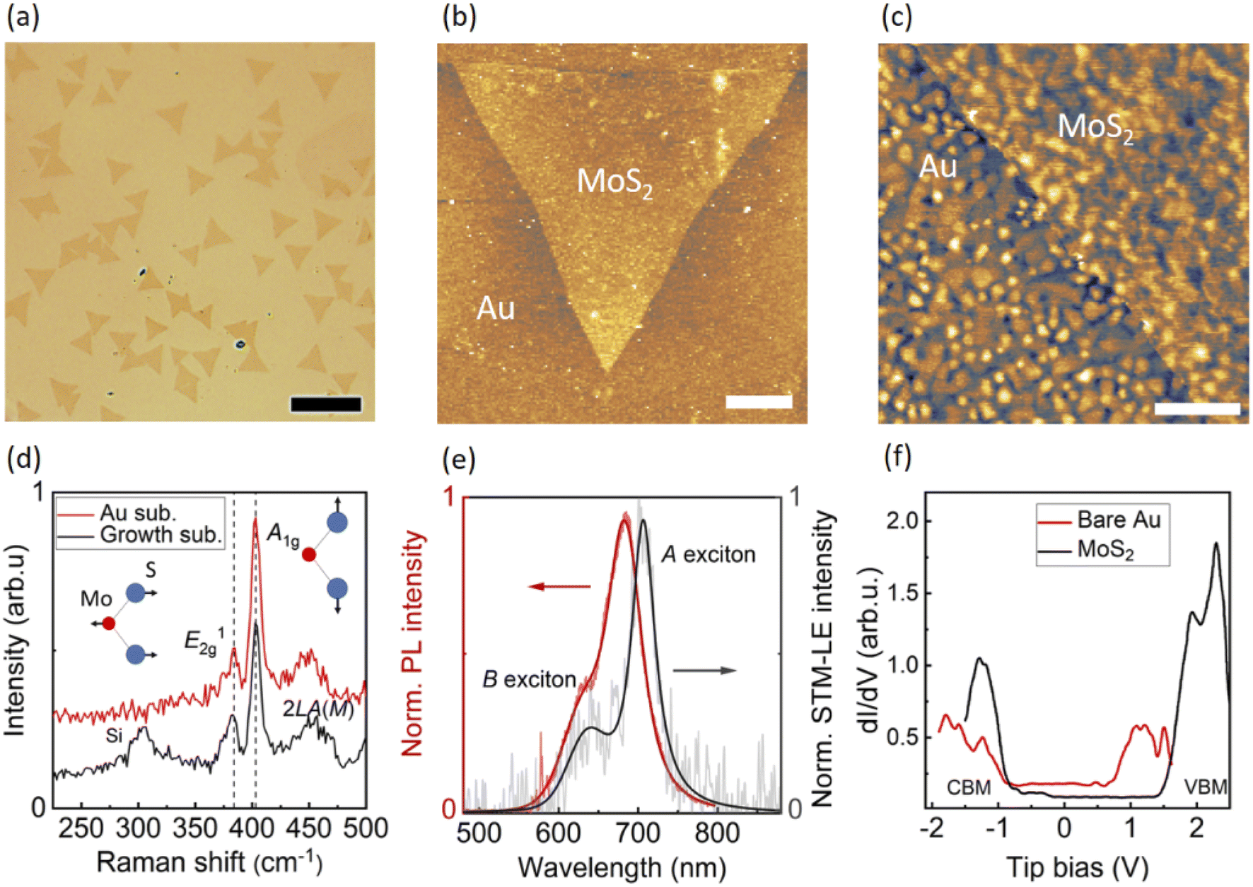 | ||
| Fig. 1 (a) Light microscopy image of typical CVD-synthesized monolayer MoS2 flakes transferred onto the evaporated gold substrate. Scale bar: 20 μm. (b) AFM topography of a monolayer MoS2 flake on the gold substrate. Scale bar: 2 μm. (c) STM topography obtained with a tip bias of −3 V and a tunneling current of 100 pA. Scale bar: 200 nm. (d) Raman spectra of monolayer MoS2 on growth substrate (SiO2/Si) and evaporated Au substrate. (e) PL and STM-LE spectra of monolayer MoS2 on evaporated Au substrate. Both Raman and PL are acquired by an ex situ setup with an excitation laser of 561 nm wavelength. STM-LE spectrum is obtained with a tip bias of −4.5 V, tunneling current of 30 nA and integration time of 3 min. (f) Differential conductance dI/dV spectra acquired on the bare gold surface and monolayer MoS2. The corresponding CBM and VBM are found at tip bias of −0.8 eV and 1.5 eV, respectively. | ||
Fig. 1d shows the ex situ Raman spectra of monolayer MoS2 as-synthesized on the growth substrate and after transfer onto the evaporated Au substrate, both measured in air at room temperature. On both substrates, the in-plane vibration mode E12g and the out-of-plane vibration mode A1g of MoS2 are found at around 383 cm−1 and 403 cm−1, respectively. A difference of ∼20 cm−1 between the two modes is in good agreement with the typical characteristic reported for single-layer MoS2.32 The second order peak of longitudinal acoustic phonons at M point (2LA(M)) is also visible in Raman scattering.32 The absence of significant changes in the Raman spectrum after transferring MoS2 onto the Au substrate points to an electronic decoupling from the metallic surface by the water clusters.25 Fig. 1e shows the ex situ PL and STM-LE spectra of the same monolayer MoS2 on evaporated Au substrate. The intense PL peak at ∼683 nm arises from the radiative recombination of A excitons,2 and the A peak in the STM-LE spectrum is found at ∼706 nm. The secondary STM-LE peak at a shorter wavelength (∼635 nm), blue-shifted by about 0.2 eV from the A peak, is assigned to the radiative decay of B excitons. This energy shift matches the valence band splitting energy induced by strong spin–orbit coupling in monolayer MoS2.33,34 This B exciton emission also contributes to the shoulder in the PL spectrum.
Owing to the different excitation methods, the PL spectrum presents the overall optical behavior of an area several hundred nanometers in diameter, while the STM-LE derives from local excitation on the nanometer scale. To better understand the spectral shift between PL and STM-LE spectra, we investigated PL of monolayer MoS2 flakes on different substrates (Fig. S2).† Monolayer MoS2 as-synthesized on the growth substrate and after transfer onto a fresh 300 nm SiO2/Si substrate show similar PL peaks. The slight broadening after transfer may be caused by the introduction of charges or defects during the transfer process.35 After transfer onto rough surfaces, i.e., evaporated Au or indium tin oxide (ITO)-coated glass, the PL spectra of monolayer MoS2 exhibit red-shifts due to the strain introduced by the corrugated surface, as already reported previously.36 The larger PL red-shift of monolayer MoS2 on ITO compared to that of MoS2 on evaporated Au is in good accordance with previously reported results since ITO has a rougher surface.36 Consequently, we attribute the observed difference in peak wavelengths between the PL and STM-LE spectra to the local strain-induced exciton modulation resolved by STM-LE, which will be discussed in more detail below. The broadening of the PL on rough substrates may also result from the strain distribution in MoS2.
First, we turn to the characterization of electronic properties of monolayer MoS2 by scanning tunneling spectroscopy (STS) (see Fig. 1f). The reference dI/dV spectrum on bare evaporated Au shows the characteristic surface state at around 0.5 V tip bias. The dI/dV spectrum of MoS2 displays clear band edges: conduction band minimum (CBM) and valence band maximum (VBM) at around −0.8 V and 1.5 V, respectively, indicating the electronic band gap of the monolayer MoS2 to be 2.30 ± 0.09 eV (3 measurements). The corresponding A exciton binding energy (i.e., the energy difference between the electronic band gap and the optical gap) is ≈ 0.5 eV resulting from an STM-LE A peak of ∼1.8 eV at the measured sample location. The electronic band gap of our monolayer MoS2 is closer to the band gap of ≈2.5 eV of suspended monolayer MoS2,37 in contrast to a band gap of 1.74 eV from epitaxial monolayer MoS2 grown directly on Au.38 For epitaxial MoS2 on Au, the interaction between the metal substrate and MoS2 leads to hybridization of the states and a lower band gap.38 The measured electronic band gap of our monolayer MoS2 on Au provides further evidence of decoupling water clusters in between.
We now compare the STM-LE of bare Au surface and monolayer MoS2. The light emission from the Au surface (Fig. S3†) is attributed to the radiative decay of gap plasmons, which are sensitive to the local geometry and dielectric properties.39 STM-LE spectra of monolayer MoS2 acquired at fixed sample location for both bias polarities are shown in Fig. S4.† For low tip bias voltage, there is only one emission peak from the plasmonic radiative decay. With increasing voltage, a second peak appears at a shorter wavelength, corresponding to the excitonic radiative decay of MoS2, which barely shifts when tip bias is high. Despite its presence, the plasmonic background does not hinder the study of the optical properties of monolayer MoS2, as the plasmonic background is weaker than the excitonic emission at high tip bias (>3 V).
The photon emission quantum efficiency of MoS2 is obtained by simultaneously scanning the sample surface with STM tip and recording the photon number with the photon counter. With a tip bias of −3.25 V, the averaged photon count is 350 s−1nA−1 (Fig. S5†). Accounting for the geometric collection efficiency of the lens system and the photon counter's detection efficiency, the quantum efficiency (QE) of STM-LE of monolayer MoS2 is estimated to be 3.7 × 10⁻⁶ photons per electron, similar to the value reported for MoSe2/Au (∼4 × 10⁻⁶ photons per electron).24
Tunneling current-induced exciton emission
Exciton emission of TMDCs has been reported to depend on current. Examples include multiple-exciton–exciton interactions in a MoS2 diode30 and neutral exciton and trion emission controlled by tunneling current.25 Using STM-LE, we studied the influence of local tunneling current and tip bias on exciton emission from monolayer MoS2. The STM-LE spectra acquired at a fixed sample location with a constant tip bias are shown in Fig. 2a. The spectra indicate a systematic change of exciton emission with different current settings. When the tunneling current is around 20 nA, the spectrum only shows one emission peak, corresponding to the A exciton recombination. The B peak appears for higher tunneling currents. For the current and bias ranges probed in our measurements, tunneling current only influences the exciton emission intensity but not the exciton energy, as the spectral peaks do not shift with different current settings. Fig. 2b further shows that the tip bias does not affect the exciton energy. | ||
| Fig. 2 The influences of tunneling current and tip bias on STM-LE spectra of monolayer MoS2. (a) Normalized STM-LE spectra acquired at a fixed sample location with different tunneling currents. Tip bias: −4 V. The spectra are well fitted with two Lorentzian peaks associated with A exciton (dark pink) and B exciton (light pink). (b) Normalized STM-LE spectra at a fixed sample location of MoS2 with varying tip biases. Tunneling current: 30 nA. (c) and (d) show the current-dependent intensities for A and B excitons, respectively. The intensities are extracted from fitted spectra obtained at different locations on the same MoS2 flake. The data in (d) is fitted linearly. | ||
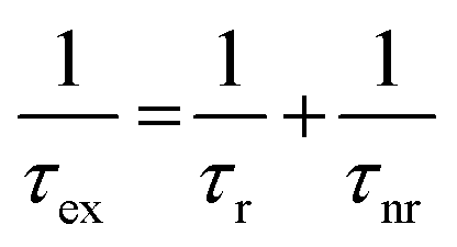
Understanding the exciton dynamics of monolayer MoS2 is essential for device development. The current-dependent emission intensities of A and B excitons are presented in Fig. 2c and d. The STM-LE intensity is related to the exciton lifetime (τex), which depends on the radiative and nonradiative exciton decay through:40
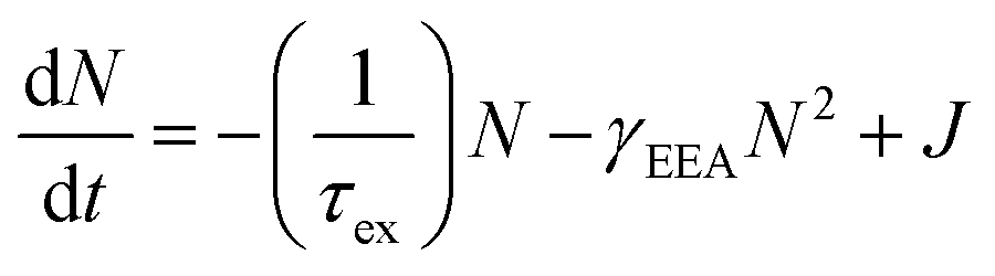
In Fig. 2, the B peak intensity shows a linear dependence on the tunneling current in the range of 20 nA–60 nA. In contrast, A peak intensity saturates under high tunneling currents. This saturation of A peak intensity can be explained by the non-linear process of exciton–exciton annihilation (EEA), which has been widely observed in monolayer TMDCs in photoluminescence measurements.40,44 For high exciton density, EEA opens an additional path for non-radiative exciton decay. In steady state, the rate of change in the population N of excitons excited by tunneling current injection can be described as:44
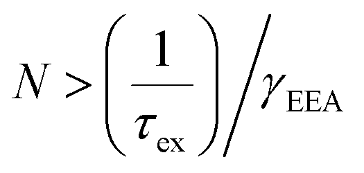 ), EEA becomes the major exciton decay process, causing the current-dependent STM-LE intensity to deviate from the linear trend.
In our measurements, the required injection current for A exciton to reach the EEA-dominated population regime is lower than that for B exciton. This difference can be explained by the different exciton lifetimes and EEA rates between A and B excitons. Particularly, the rapid relaxation (∼ps) from B exciton to A exciton reduces the B exciton population and simultaneously increases the A exciton population.45 This rapid relaxation also explains the higher intensity of the A peak compared to the weak B peak at low currents before reaching the EEA-dominated regime. More quantitative analysis of exciton dynamics would require ultrafast time-resolved spectroscopy, which is beyond the scope of our setup. Knowing the EEA rate helps control the excitation injection to maintain an optimal light emission efficiency of TMDCs.
Strain-induced exciton emission
Monolayer MoS2 exhibits high mechanical flexibility.46 Placed on an evaporated Au substrate, van der Waals interactions make the as-grown planar monolayer MoS2 conform to the local surface corrugation, which causes locally varying levels of strain. No wrinkles or bubbles are observed after transfer by optical microscopy and AFM. We assume the strain is mainly introduced by the surface roughness of the Au substrate. Strain tunes the electronic band gap but not the binding energy of excitons.17,18,47 Thus, we observe significant peak shifts of exciton emission as shown in Fig. 3, where STM-LE spectra are acquired at sample locations separated by 10 nm.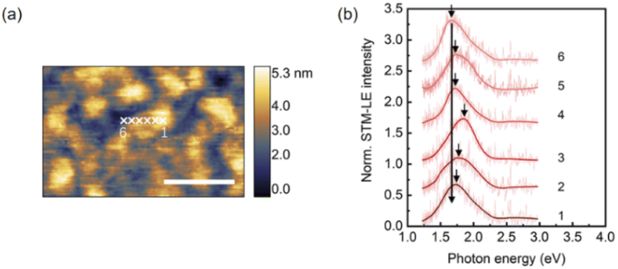 | ||
| Fig. 3 The influence of substrate topography on STM-LE spectra of monolayer MoS2. (a) and (b) show STM topography and STM-LE spectra, respectively. The spectra are obtained at six sample locations separated by 10 nm as marked in (a). STM parameters: −3 V tip bias, and 100 pA tunneling current. Scale bar: 100 nm. STM-LE parameters: −4 V tip bias, 30 nA tunneling current, and 3 min integration time. | ||
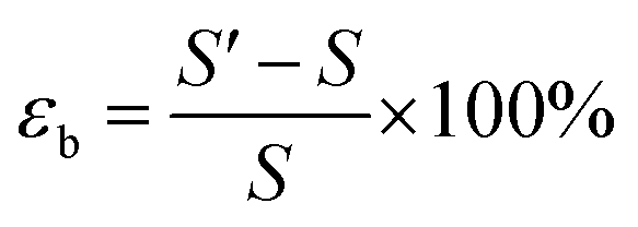
Assuming that shear strain components are negligible, biaxial strain εb takes the simple form of εxx + εyy, where εxx and εyy are the strain components in the x and y directions.48,49 To derive the sum of these two strain components from local surface topography, we compare the actual surface area of MoS2 and its projected area, as shown in Fig. S7.† To this end, a Gaussian filter is applied to the local surface topography to generate smooth surfaces. Then, to first order approximation, the tensile biaxial strain is obtained by:
 | ||
| Fig. 4 The influence of strain on STM-LE spectra of MoS2. (a) STM image of monolayer MoS2 acquired with a tip bias of −3 V and a tunneling current of 100 pA. Scale bar: 100 nm. (b) AFM image of MoS2 at the same sample region as (a). Scale bar: 100 nm. (c) Strain map and (d) corresponding A peak wavelength map acquired at the region indicated by the white box in (a). The pixel size is 10 × 10 nm2. The exciton energies are determined by fitting the spectra with Lorentzian profiles. STM-LE parameters: −4 V tip bias, 30 nA tunneling current, and 3 min integration time. | ||
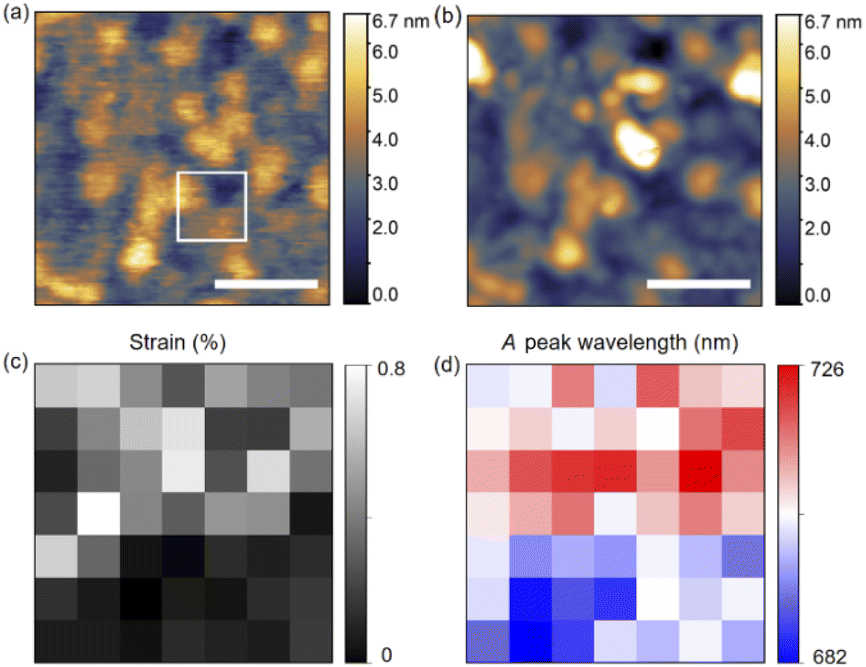
Fig. 5 shows the variation of measured peak energies with local curvature induced strain. Fig. 5a displays the plasmonic peak energy of the bare Au substrate versus a virtual ‘strain’ value, calculated by the same method described above for MoS2. The absence of a clear trend in energy variation over a range of local curvatures is evident. We attribute the comparatively wide distribution of peak energies for identical virtual ‘strain’ values to local variations in the plasmonic tip–sample cavity. In contrast, A exciton peak energy of MoS2, shown in Fig. 5b, exhibits a clear linear modulation rate of −69 ± 5 meV/% with a Pearson correlation coefficient of −0.87. This modulation rate is in good agreement with the result obtained by diffraction-limited photoluminescence of CVD monolayer MoS2 upon biaxial strain (a value of −76 ± 10 meV/%).48 Considering the absence of a trend on the bare Au substrate and the electronic decoupling of monolayer MoS2 from the Au substrate by a thin water spacer, the observed linear modulation of A exciton energy can be assigned to the local strain variations in MoS2, induced by the corrugated surface. Moreover, spectra acquired on other monolayer MoS2 flakes wet-transferred from the same CVD-synthesis have closely matching values for the strain modulation rates (Fig. S8†).
 | ||
| Fig. 5 (a) Peak energy of STM-LE on the bare gold surface with different local curvature. (b) A exciton energy of MoS2 with different local strains induced by curvature. Inserts show the corresponding STM images. Scale bar: 20 nm. The pixel size for each data point is 10 × 10 nm2. The data points are fitted linearly with Pearson correlation coefficients of 0.06 and −0.87 for (a) and (b), respectively. The modulation rate of strain on A exciton is estimated as −69 ± 5 meV/%. | ||
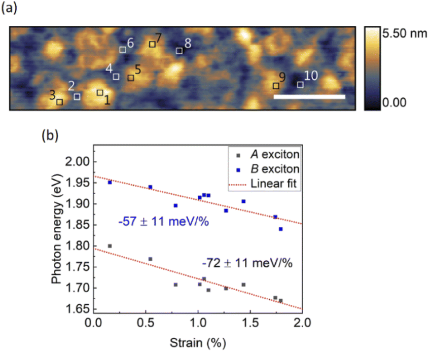 | ||
| Fig. 6 Strain-modulated A and B excitonic luminescence. (a) STM image of monolayer MoS2 on Au surface. Tip bias: −3 V, tunneling current: 100 pA, scale bar: 100 nm. (b) A and B exciton energies as functions of strain, acquired at the locations indicated by the boxes in (a). Tip bias: −4 V, tunneling current: 50 nA, integration time: 3 min. | ||
Discussion
Two possible excitation mechanisms can be involved in STM-LE: (i) diodelike excitation through electron and hole injections25,51,52 and (ii) resonance energy transfer by virtual photon coupling.23 The diodelike excitation mechanism generally requires a luminescence onset electron energy (i.e. tip bias) higher than the ‘free particle’ electronic bandgap energy of monolayer MoS2. In the resonance energy transfer mechanism, the onset of luminescence occurs at an electron energy surpassing the optical gap energy. In our work, the onset of luminescence of MoS2 (Fig. S4†) occurs at a negative tip bias close to the optical gap of monolayer MoS2, indicating that the luminescence is excited by virtual photon coupling. Due to the limited sensitivity of our spectrometer, all STM-LE spectra were acquired with a tip bias higher than the electronic bandgap of monolayer MoS2, where both excitation processes may be present.For the range of tip bias and current applied in our experiments, STM-LE spectra show no systematic peak shifts at fixed locations for varying tip bias or tunneling current. This holds both for plasmonic emission from the bare Au substrate and excitonic emission from MoS2. Hence, the tunneling gap or the electric field have little influence on the exciton energies of MoS2. The presence of water clusters between Au substrate and MoS2 effectively decouples the two materials electronically, allowing one to directly probe the excitonic emission of MoS2. The spectral shifts in excitonic luminescence in monolayer MoS2 are directly related to alterations of the electronic bandgap induced by strain.
In strain-engineered 2D materials, thermal scanning probe lithography has recently achieved a strain pattern with 20 nm resolution.22 It is challenging to adequately resolve such a fine pattern by far-field optical excitation methods. Local excitation as in STM-LE offers a powerful alternative. However, excitons may diffuse up to 2 μm away from the location of excitation before radiative decay occurs at room temperature.23 By locally modifying the electronic band gap of 2D materials, strain also can introduce funnel centers towards which excitons drift before recombination.21 Thus, resolving local strain via spectral signatures requires consideration of the measuring methods and the exciton dynamics. In our experiments, taking advantage of STM-LE, local strain changes in monolayer MoS2 can be distinguished on a length scale of 10 nm, as evidenced in Fig. 3 and 4.
Conclusion
STM-LE is a powerful technique to probe excitons in confined semiconductors with nanometer lateral resolution. In this work, we present a study of the excitonic luminescence of monolayer MoS2 on an evaporated gold thin film substrate, locally excited by an STM tip. Due to the water spacer between substrate and MoS2, electronic coupling between substrate and MoS2 is negligible, allowing one to investigate the excitonic emission of monolayer MoS2 despite the presence of a plasmonic background. The luminescent spectra from monolayer MoS2 are attributed to the radiative recombination of A and B excitons. Both A and B excitonic peaks show energy shifts due to the local strain introduced by the corrugated substrate. Additionally, the emission intensities of A and B excitons depend on tunneling current. Thus, by tuning the tunneling current, the luminescence spectra can be adapted to different investigations. For instance, the local strain distribution of monolayer MoS2 can be probed with a low tunneling current through analyzing the A exciton energy, which avoids long-term heating. Exciton energies and dynamics (in particular, exciton lifetimes) can be explored with high tunneling currents, where both A and B exciton emissions are detectable. In addition to investigating the optoelectronic properties of 2D materials, STM-LE also enables one to perform local analyses of strain or material deformation in piezoelectrical53,54 and piezo-resistive devices.55Experimental
Materials
Sulfur (S) powder (99.98%, Sigma-Aldrich, CAS: 7704-34-9) and sodium molybdate (Na2MoO4) powder (≥98%, Sigma-Aldrich, CAS: 7631-95-0) were used as delivered and not purified further. The MoS2 flakes were grown on a Si(100) n-type substrate, covered with a 300 nm thick SiO2 layer, and synthesized in a 1-inch single heating zone tube furnace (Lindberg/Blue M). Quality and thickness of flakes were investigated by optical microscopy and atomic force microscopy.Methods
STM-LE setup
STM-LE experiments were conducted at room temperature in high vacuum (10−7 mbar), using a custom-built STM instrument. An aspheric lens (Thorlabs A110-B, NA 0.40) mounted at an incident angle of 60° from the sample normal collects the emitted light. In the case of isotropic radiation, the hemisphere photon collection efficiency is about 8.3%. However, the light emission pattern is modified by the tip-sample junction and the orientations of the luminescent exciton/dipole.57,58 Thus, the collection efficiency could be higher due to the angle-dependent emission pattern. In our experiments, we estimate the final detection efficiency of the optical system by only considering isotropic radiation. An optical fiber (Schaefter + Kirchhoff V-KF40-2x-MMC-VIS/NIR-105-NA022) guides the light out of the vacuum chamber to detectors. The STM-LE is either recorded by a photon counter (Hamamatsu C1300-1) or a spectrograph (Princeton Instrument SP2156i, with a 150 lines/mm grating) and a cooled CCD camera (PCO 2000) or a cooled EMCCD (Andor Newton 970P). The differential conductance dI/dV is measured by STS with a lock-in amplifier (modulation voltage: 50 mV, and frequency: 470 Hz). All STM measurements are acquired with platinum/iridium (90![[thin space (1/6-em)]](https://www.rsc.org/images/entities/char_2009.gif) :10) tips prepared by electrochemical etching in CaCl2 solution. The STM tips have radii of 50∼100 nm supporting lateral resolution in the few nm range. Additionally, surface topography is acquired by an atomic force microscope (AFM) (Oxford Instruments, Cypher).
:10) tips prepared by electrochemical etching in CaCl2 solution. The STM tips have radii of 50∼100 nm supporting lateral resolution in the few nm range. Additionally, surface topography is acquired by an atomic force microscope (AFM) (Oxford Instruments, Cypher).
Raman and PL setup
Both Raman and PL measurements were performed in air at ambient condition by a NT-MDT Raman system equipped with a 100× objective (NA = 0.8), using an excitation laser of 561 nm. Gratings: 150 lines/mm (PL measurement) and 600 lines/mm (Raman measurement) were used.Conflicts of interest
There are no conflicts to declare.Acknowledgements
The authors gratefully acknowledge the technical support of Blerim Veselaj (Nanotechnology Group, ETH Zurich), and the support of the BRNC cleanroom staff.References
- A. Splendiani, L. Sun, Y. Zhang, T. Li, J. Kim, C. Y. Chim, G. Galli and F. Wang, Nano Lett., 2010, 10, 1271–1275 CrossRef CAS PubMed.
- K. F. Mak, C. Lee, J. Hone, J. Shan and T. F. Heinz, Phys. Rev. Lett., 2010, 105, 136805 CrossRef PubMed.
- W. Zhao, Z. Ghorannevis, L. Chu, M. Toh, C. Kloc, P. H. Tan and G. Eda, ACS Nano, 2013, 7, 791–797 CrossRef CAS PubMed.
- T. Cheiwchanchamnangij and W. R. L. Lambrecht, Phys. Rev. B, 2012, 85, 205302 CrossRef.
- A. Chernikov, T. C. Berkelbach, H. M. Hill, A. Rigosi, Y. Li, O. B. Aslan, D. R. Reichman, M. S. Hybertsen and T. F. Heinz, Phys. Rev. Lett., 2014, 113, 076802 CrossRef CAS PubMed.
- K. He, N. Kumar, L. Zhao, Z. Wang, K. F. Mak, H. Zhao and J. Shan, Phys. Rev. Lett., 2014, 113, 026803 CrossRef CAS PubMed.
- O. Lopez-Sanchez, D. Lembke, M. Kayci, A. Radenovic and A. Kis, Nat. Nanotechnol., 2013, 8, 497–501 CrossRef CAS PubMed.
- M. Amani, D. H. Lien, D. Kiriya, J. Xiao, A. Azcatl, J. Noh, S. R. Madhvapathy, R. Addou, S. KC, M. Dubey, K. Cho, R. M. Wallace, S. C. Lee, J. H. He, J. W. Ager, X. Zhang, E. Yablonovitch and A. Javey, Science, 2015, 350, 1065–1068 CrossRef CAS PubMed.
- D. Xiao, G.-B. Liu, W. Feng, X. Xu and W. Yao, Phys. Rev. Lett., 2012, 108, 196802 CrossRef PubMed.
- X. Xu, W. Yao, D. Xiao and T. F. Heinz, Nat. Phys., 2014, 10, 343–350 Search PubMed.
- A. Pospischil, M. M. Furchi and T. Mueller, Nat. Nanotechnol., 2014, 9, 257–261 CrossRef CAS PubMed.
- J. S. Ross, P. Klement, A. M. Jones, N. J. Ghimire, J. Yan, D. G. Mandrus, T. Taniguchi, K. Watanabe, K. Kitamura, W. Yao, D. H. Cobden and X. Xu, Nat. Nanotechnol., 2014, 9, 268–272 CrossRef CAS PubMed.
- Y. J. Zhang, T. Oka, R. Suzuki, J. T. Ye and Y. Iwasa, Science, 2014, 344, 725–728 CrossRef CAS PubMed.
- Z. Yin, H. Li, H. Li, L. Jiang, Y. Shi, Y. Sun, G. Lu, Q. Zhang, X. Chen and H. Zhang, ACS Nano, 2012, 6, 74–80 CrossRef CAS PubMed.
- L. Britnell, R. M. Ribeiro, A. Eckmann, R. Jalil, B. D. Belle, A. Mishchenko, Y.-J. Kim, R. V. Gorbachev, T. Georgiou, S. V. Morozov, A. N. Grigorenko, A. K. Geim, C. Casiraghi, A. H. Castro Neto and K. S. Novoselov, Science, 2013, 340, 1311–1314 CrossRef CAS PubMed.
- D. Kufer and G. Konstantatos, Nano Lett., 2015, 15, 7307–7313 CrossRef CAS PubMed.
- E. Scalise, M. Houssa, G. Pourtois, V. Afanas’ev and A. Stesmans, Nano Res., 2012, 5, 43–48 CrossRef CAS.
- H. Peelaers and C. G. Van de Walle, Phys. Rev. B, 2012, 86, 241401 CrossRef.
- K. He, C. Poole, K. F. Mak and J. Shan, Nano Lett., 2013, 13, 2931–2936 CrossRef CAS PubMed.
- H. J. Conley, B. Wang, J. I. Ziegler, R. F. Haglund Jr, S. T. Pantelides and K. I. Bolotin, Nano Lett., 2013, 13, 3626–3630 CrossRef CAS PubMed.
- H. Li, A. W. Contryman, X. Qian, S. M. Ardakani, Y. Gong, X. Wang, J. M. Weisse, C. H. Lee, J. Zhao, P. M. Ajayan, J. Li, H. C. Manoharan and X. Zheng, Nat. Commun., 2015, 6, 1–7 CAS.
- X. Liu, A. K. Sachan, S. T. Howell, A. Conde-Rubio, A. W. Knoll, G. Boero, R. Zenobi and J. Brugger, Nano Lett., 2020, 20, 8250–8257 CrossRef CAS PubMed.
- D. Pommier, R. Bretel, L. E. P. López, F. Fabre, A. Mayne, E. Boer-Duchemin, G. Dujardin, G. Schull, S. Berciaud and E. Le Moal, Phys. Rev. Lett., 2019, 123, 027402 CrossRef CAS PubMed.
- R. Péchou, S. Jia, J. Rigor, O. Guillermet, G. Seine, J. Lou, N. Large, A. Mlayah and R. Coratger, ACS Photonics, 2020, 7, 3061–3070 CrossRef.
- R. J. P. Román, Y. Auad, L. Grasso, F. Alvarez, I. D. Barcelos and L. F. Zagonel, Nanoscale, 2020, 12, 13460–13470 RSC.
- C. Große, P. Merino, A. Rosławska, O. Gunnarsson, K. Kuhnke and K. Kern, ACS Nano, 2017, 11, 1230–1237 CrossRef PubMed.
- B. Doppagne, M. C. Chong, E. Lorchat, S. Berciaud, M. Romeo, H. Bulou, A. Boeglin, F. Scheurer and G. Schull, Phys. Rev. Lett., 2017, 118, 127401 CrossRef PubMed.
- Y. Z. Ma, L. Valkunas, S. L. Dexheimer, S. M. Bachilo and G. R. Fleming, Phys. Rev. Lett., 2005, 94, 157402 CrossRef PubMed.
- F. Wang, Y. Wu, M. S. Hybertsen and T. F. Heinz, Phys. Rev. B, 2006, 73, 245424 CrossRef.
- Y. Ye, Z. Ye, M. Gharghi, H. Zhu, M. Zhao, Y. Wang, X. Yin and X. Zhang, Appl. Phys. Lett., 2014, 104, 193508 CrossRef.
- M. Hong, P. Yang, X. Zhou, S. Zhao, C. Xie, J. Shi, Z. Zhang, Q. Fu and Y. Zhang, Adv. Mater. Interfaces, 2018, 5, 1800641 CrossRef.
- H. Li, Q. Zhang, C. C. R. Yap, B. K. Tay, T. H. T. Edwin, A. Olivier and D. Baillargeat, Adv. Funct. Mater., 2012, 22, 1385–1390 CrossRef CAS.
- R. Coehoorn, C. Haas and R. A. de Groot, Phys. Rev. B, 1987, 35, 6203 CrossRef CAS PubMed.
- W. Zhao, R. M. Ribeiro, M. Toh, A. Carvalho, C. Kloc, A. H. Castro Neto and G. Eda, Nano Lett., 2013, 13, 5627–5634 CrossRef CAS PubMed.
- M. Buscema, G. A. Steele, H. S. van der Zant and A. Castellanos-Gomez, Nano Res., 2014, 7, 561–571 CrossRef.
- W. H. Chae, J. D. Cain, E. D. Hanson, A. A. Murthy and V. P. Dravid, Appl. Phys. Lett., 2017, 111, 143106 CrossRef.
- A. R. Klots, A. K. M. Newaz, B. Wang, D. Prasai, H. Krzyzanowska, J. Lin, D. Caudel, N. I. Ghimire, J. Yan, B. L. Ivanov, K. A. Velizhanin, A. Burger, D. G. Mandrus, N. H. Tolk, S. T. Pantelides and K. I. Bolotin, Sci. Rep., 2014, 4, 6608 CrossRef CAS PubMed.
- A. Bruix, J. A. Miwa, N. Hauptmann, D. Wegner, S. Ulstrup, S. S. Grønborg, C. E. Sanders, M. Dendzik, A. G. Cabo, M. Bianchi, J. V. Lauritsen, A. A. Khajetoorians, B. Hammer and P. Hofmann, Phys. Rev. B, 2016, 93, 165422 CrossRef.
- R. Berndt, J. K. Gimzewski and P. Johansson, Phys. Rev. Lett., 1993, 71, 3493 CrossRef CAS PubMed.
- L. Yuan and L. Huang, Nanoscale, 2015, 7, 7402–7408 RSC.
- M. Palummo, M. Bernardi and J. C. Grossman, Nano Lett., 2015, 15, 2794–2800 CrossRef CAS PubMed.
- H. Wang, C. Zhang and F. Rana, Nano Lett., 2015, 15, 339–345 CrossRef CAS PubMed.
- Y. Yu, Y. Yu, C. Xu, Y. Q. Cai, L. Su, Y. Zhang, Y. W. Zhang, K. Gundogdu and L. Cao, Adv. Funct. Mater., 2016, 26, 4733–4739 CrossRef CAS.
- Y. Yu, Y. Yu, C. Xu, A. Barrette, K. Gundogdu and L. Cao, Phys. Rev. B, 2016, 93, 201111 CrossRef.
- K. M. McCreary, A. T. Hanbicki, S. V. Sivaram and B. T. Jonker, APL Mater., 2018, 6, 111106 CrossRef.
- J. Pu, Y. Yomogida, K. K. Liu, L. J. Li, Y. Iwasa and T. Takenobu, Nano Lett., 2012, 12, 4013–4017 CrossRef CAS PubMed.
- H. Shi, H. Pan, Y. W. Zhang and B. I. Yakobson, Phys. Rev. B, 2013, 87, 155304 CrossRef.
- A. Michail, D. Anestopoulos, N. Delikoukos, J. Parthenios, S. Grammatikopoulos, S. A. Tsirkas, N. N. Lathiotakis, O. Frank, K. Filintoglou and K. Papagelis, 2D Mater., 2021, 8, 015023 CrossRef CAS.
- L. Lăzărescu, D. S. COMŞA, I. Nicodim, I. Ciobanu and D. Banabic, Trans. Nonferrous Met. Soc. China, 2012, 22, s275–s279 CrossRef.
- S. D. Guo, Comput. Mater. Sci., 2016, 123, 8–13 CrossRef CAS.
- X. H. Qiu, G. V. Nazin and W. Ho, Science, 2003, 299, 542–546 CrossRef CAS PubMed.
- R. Cheng, D. Li, H. Zhou, C. Wang, A. Yin, S. Jiang, Y. Liu, Y. Chen, Y. Huang and X. Duan, Nano Lett., 2014, 14, 5590–5597 CrossRef CAS PubMed.
- H. Zhu, Y. Wang, J. Xiao, M. Liu, S. Xiong, Z. J. Wong, Z. Ye, Y. Ye, X. Yin and X. Zhang, Nat. Nanotechnol., 2015, 10, 151–155 CrossRef CAS PubMed.
- X. Wang, X. He, H. Zhu, L. Sun, W. Fu, X. Wang, L. C. Hoong, H. Wang, Q. Zeng, W. Zhao, J. Wei, Z. Jin, Z. Shen, J. Liu, T. Zhang and Z. Liu, Sci. Adv., 2016, 2, e1600209 CrossRef PubMed.
- W. Li, M. Dai, Y. Hu, H. Chen, X. Zhu, Q. Yang and P. Hu, ACS Appl. Mater. Interfaces, 2019, 11, 47098–47105 CrossRef CAS PubMed.
- L. Jiao, B. Fan, X. Xian, Z. Wu, J. Zhang and Z. Liu, J. Am. Chem. Soc., 2008, 130, 12612–12613 CrossRef CAS PubMed.
- J. A. Schuller, S. Karaveli, T. Schiros, K. He, S. Yang, I. Kymissis, J. Shan and R. Zia, Nat. Nanotechnol., 2013, 8, 271–276 CrossRef CAS PubMed.
- O. J. F. Martin and C. Girard, Appl. Phys. Lett., 1997, 70, 705–707 CrossRef.
Footnote |
| † Electronic supplementary information (ESI) available. See https://doi.org/10.1039/d2ra05123k |
| This journal is © The Royal Society of Chemistry 2022 |