
 Open Access Article
 This Open Access Article is licensed under a Creative Commons Attribution-Non Commercial 3.0 Unported Licence
Use of dielectrophoresis for directing T cells to microwells before nanostraw transfection: modelling and experiments†
Mercy Lard,
Bao D. Ho ,
Jason P. Beech,
Jonas O. Tegenfeldt and
Christelle N. Prinz*
,
Jason P. Beech,
Jonas O. Tegenfeldt and
Christelle N. Prinz*
Division of Solid State Physics and NanoLund, Lund University, 221 00 Lund, Sweden. E-mail: christelle.prinz@ftf.lth.se
First published on 24th October 2022
Abstract
Nanostraw substrates have great potential for achieving minimally invasive cell transfection. Cells located on the nanostraw substrate are subjected to mild DC electric pulses applied across the nanostraw substrate, which open pores in the cell membrane on top of the nanostraws and drives charged cargo through these pores via electrophoresis. However, with this method, the current may leak through uncovered nanostraws, thereby decreasing the desired effect in the cell-covered nanostraws. A minimization of the number of uncovered nanostraws could be achieved by high cell coverage, but this is challenging when working with small cell populations. Nanostraw substrates of smaller area could be covered by smaller cell populations but are hard to integrate into fluidics systems. Here, we use simulations and experiments to show that this issue can be addressed by covering the nanostraw substrate with an insulating layer containing pores of similar size to cells. The pores act as traps into which cells can be guided using dielectrophoresis, ensuring a high degree of occupancy while maintaining a high cell viability, even if the total number of cells is low.
Introduction
Nanostraw-assisted intracellular injection is a method increasingly used for transporting cargos into cells with minimal detrimental effect on cell function.1–4 The method, introduced in 2012,1 has since had its efficiency improved by combination with electrical pulses2 and can be used for both adherent and non-adherent cells. Nanostraw injection has been shown to be superior to other delivery methods such as electroporation and lipofection in terms of delivery efficiency and non invasiveness.3,5 During nanostraw-assisted injection, cells are cultured or centrifuged onto a substrate with protruding nanostraws that provide fluidic connection to the back side of the substrate. Cargos are loaded in the reservoir on the backside of the nanostraw substrate and transported through the nanostraws to the cytosol by the application of mild electrical pulses across the nanostraw substrate.2 These electrical pulses have two functions: (i) they act as local electroporation pulses, creating pores in the cell membrane that interfaces the nanostraws and (ii) they drive the electrophoretic transport of cargo through the nanostraws, from the back side reservoirs to the cytosol. Pulse amplitude, duration, and frequency all affect the resulting injection efficiency.6 Importantly, in order to successfully deliver cargos inside cells, the number of nanostraws that are not interfaced with cells should be minimized. Indeed, free nanostraws represent a low impedance path for the current flow and having too many free nanostraws leads to a voltage drop across the substrate, resulting in poor cargo delivery efficiency.7 In order to address this issue, the proportion of the nanostraw-substrate area that is covered with cells is maximized by performing centrifugation of a great number of cells on the substrate.5 However, this protocol is not compatible with cases where low number of cells are available, for instance for circulating tumor cells and antigen specific T cells. Moreover, the centrifugation step represents an extra, cumbersome experimental step which does not allow cells to be directed to specific regions on the substrate. Minimizing the size of the substrate can go some way towards minimizing the numbers of cells required for coverage but as substrates become smaller, integration into fluidics systems becomes increasingly difficult. In this paper, we use finite element simulations combined with experiments to explore whether the active area of a nanostraw substrate can be decreased independently of the total area using a second porous layer, and whether dielectrophoresis (DEP) can guide cells into the pores, making the nanostraw method relevant even in cases where too few cells are available to cover the substrate, and/or in cases where centrifugation should be avoided. DEP describes the movement of polarizable objects in an electric field gradient (see Results and discussion section for more details, as well as some relevant textbooks8,9). Objects with a higher permittivity than the surrounding medium are attracted to regions where the electric field has a maximum (positive DEP) and objects with a lower permittivity than the surrounding medium are attracted to regions where the electric field has a minimum (negative DEP). DEP has been used extensively in biological applications, to trap linear DNA, chromosomes and cells.10–13 The field gradient can be achieved by using a specific pattern of electrodes, or by using dielectric features to concentrate the field lines while using distant electrodes.For simplicity, we opted for the latter and show that it is possible to create an array of DEP traps (referred to as microwells), that are similar in size to cells and with nanostraws at the bottom, using a simple two-layer approach, with two dielectric membranes, atomic layer deposition and etching. The microwells simultaneously minimize the active area of the substrate and allow for the use of DEP to maximize nanostraw occupancy, removing the need for centrifugation. Simulations show that the electric field gradient imposed by the microwell geometry allows cells to be attracted to the microwells by means of positive dielectrophoresis and we test the device using positive DEP to direct Jurkat T cells to the microwells. DEP traps the cells in position within the microwells from where they can sediment onto the nanostraws when DEP is removed. Subsequently, as a test of delivery, propidium iodide (PI) was injected into the cytosol through the nanostraws using electrical pulses.
Experimental
Microwell-nanostraw device fabrication and assembly
Fig. 1a shows a schematics of the microwell-nanostraw device fabrication steps. Two polycarbonate track etched membranes, one 35 μm thick with pores of diameter D = 15 μm and pore density of 105 cm−2, and one 25 μm thick with pores of diameter D = 0.2 μm and pore density of 2 × 107 cm−2 (it4ip, Belgium) were treated with oxygen plasma (Plasma Preen) for 15 s at 5 mBar. The 2 membranes were then sealed together with heat and pressure (100 °C at 15 Bar for 180 s) using a nanoimprint lithography tool (Obducat, Malmö, Sweden). The sealed membranes were subsequently coated with 10 nm alumina using atomic layer deposition (ALD, Savannah, Cambridge Nanotech), at 90 °C in alternating cycles of trimethylaluminum and H2O each with pulse duration of 0.02 s and 30 s waiting time in between. The resulting alumina-coated membranes were subsequently placed on a 4′′ silicon wafer (with the 0.2 μm pore membrane facing down) using an electrostatic gun to remove any air gap between the membranes and the silicon wafer. The alumina-coated membranes on the silicon substrate were etched in a two-step process using inductively coupled plasma and reactive ion etching (ICP-RIE, APEX SLR Advanced Vacuum Systems AB). In the first step, the alumina layer was removed from all horizontal surfaces by a flow of argon gas at 40 SCCM for 90 s with RIE and ICP power of 50 W and 400 W, respectively, at a process pressure of 10 mTorr, using controlled backside helium cooling with flow at 5 SCCM and process pressure at 5 Torr. This etching step leaves the alumina on all vertical surface i.e. inside the pores, unaffected. In the second step, removal of 1 μm of the polycarbonate material was achieved by a combination of SF6 at 5 SCCM and O2 at 45 SCCM for 2 min at 5 mTorr while maintaining ICP and RIE powers and He cooling, as in the first step.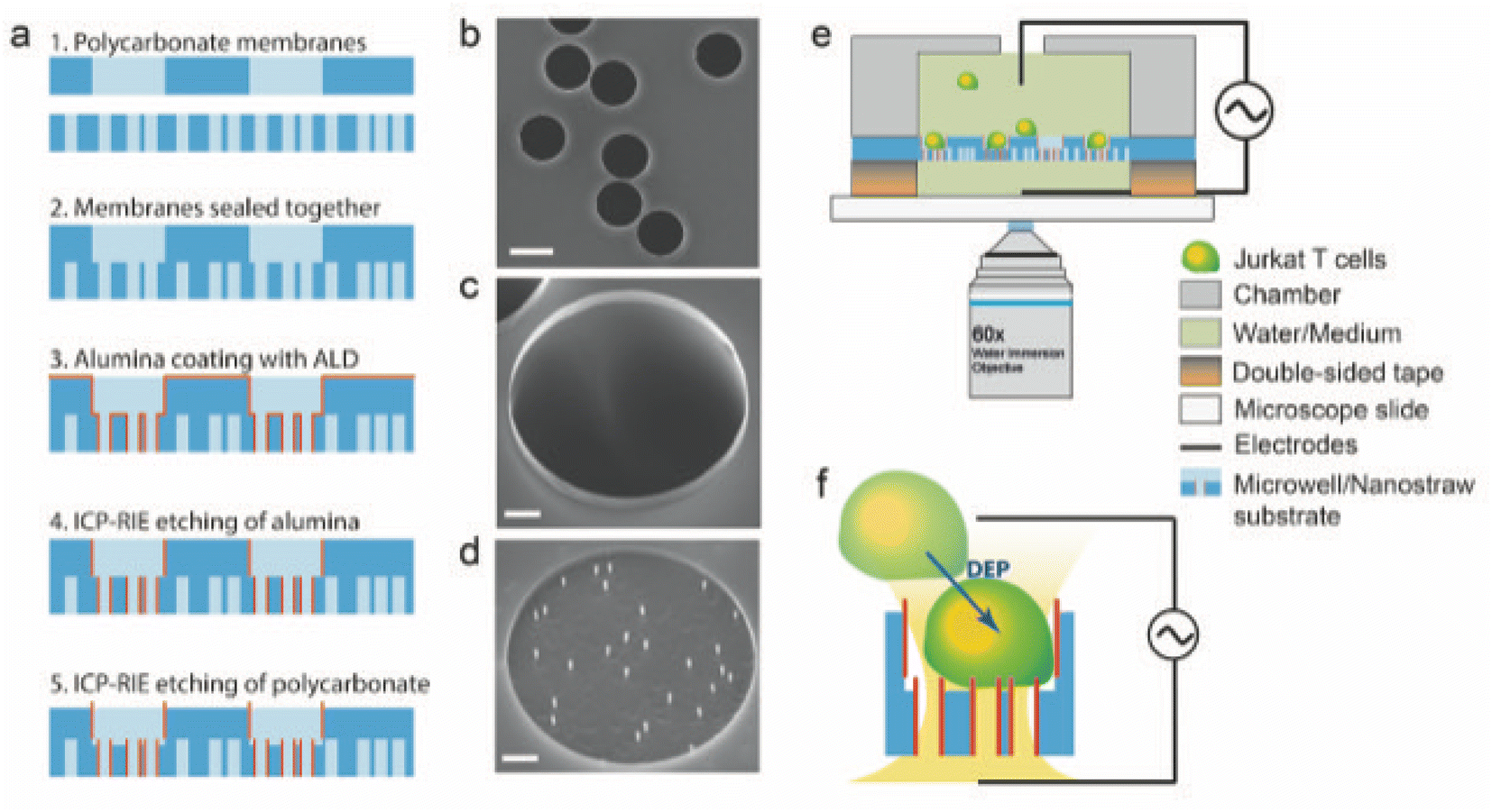 | ||
| Fig. 1 Device fabrication. (a) Schematic of the fabrication steps used to create the device. Two polycarbonate membranes are sealed together using heating and pressure, aluminum oxide is deposited using ALD, a first ICP-RIE process is performed to etch the horizontal aluminum oxide layer and a second one to specifically etch polycarbonate. (b) SEM top view of the microwells. Scale bar 15 μm (c) SEM image of a well, stage tilt 30°, scale bar 2 μm. (d) Electron microscopy image of the nanostraws at the bottom of a well. Stage tilt 30°, scale bar 2 μm. In order to be able to focus on the nanostraws, the top membrane was removed prior to SEM imaging. (e) Schematic of the device. (f) Schematic of cell trapping in the microwells using dielectrophoresis. | ||
Because the vertical alumina is not affected by this second etching step either, the exposed 1 μm of alumina forms free standing nanostraws of 0.2 μm pore diameter and 1 μm length in the bottom of 15 μm diameter microwells which we refer to as “microwell-nanostraw substrate” (Fig. 1). Note: there is a 1 μm wall of alumina around the rim of the microwells but this does not affect their function.
Fig. 1e shows a schematic of the device. A 2 by 2 cm square of the microwell-nanostraw substrate (fabrication described above) was cut and mounted onto a glass slide by placing it on 2 pads, each composed six layers of 100 μm thick double-sided tape placed at 2 opposite edges of the substrate. The pads ensures backside access to the nanostraws for inserting the lower electrode and loading the cargo solution. A cell chamber (2 cm in outer diameter with an opening of 1 cm), was attached to the top of the microwell-nanostraw substrate using silicone dental paste (equal proportion of the two components, Twinsil Speed, Picodent). The cell chamber was made with a standard clear resin (3D printed with 0.1 mm resolution on a Form 2 printer (FormLabs). The double-sided tape spacers pads were coated with dental paste to ensure that no detachment or leakage can occur during the experiments. Before each experiment, the microwell-nanostraw substrate (mounted on the glass slide) were steamed with deionized (DI) water for 5 min in order to allow for a complete wetting of the surface, thus avoiding air bubble formation. Platinum wires, 0.25 mm diameter (Merck), were used as top and bottom electrodes. A ring, approximately 7 mm in diameter was formed at one end of each wire and flattened using pliers. The electrodes were inserted below (between the pads) and above (in the cell chamber) the microwell-nanostraw substrate.
Cells and cell culture
Jurkat T cells were chosen as a well accepted cell line used for studying human T lymphocyte and T cell signaling14,15 Jurkat E6.1 (ECACC 88042803) Human Leukaemic cells were purchased from Sigma Aldrich and cultured according to standard protocols in a sterile environment. RPMI 1640 (ATCC modification, ThermoFisher Scientific) was combined with 10% fetal bovine serum (FBS, certified, USA origin, ThermoFisher Scientific) and 1% penicillin–streptomycin (Sigma Aldrich), hereafter referred to as full cell medium. Cells were maintained in an incubator with 5% CO2 at 37 °C and split by taking 2 mL of existing cells in full cell medium and adding it to 10 mL of pre-warmed fresh full cell medium every two to three days.DEP trapping
Low conductivity DEP buffer was prepared by mixing 25 μL of full cell medium (corresponding to RPMI 1640 with 10% fetal bovine serum and 1% penicillin–streptomycin). With 800 μL of 0.3 M D-mannitol (Sigma Aldrich) in DI sterilized water. Adding D-mannitol was necessary to compensate for the low osmolarity of the buffer due to its low salt concentration. Cells were centrifuged at 150 g for 5 min and resuspended in the low conductivity buffer at a concentration of approximately 106 cells per mL. Cells in low conductivity buffer were loaded to the cell chamber on top of the microwell-nanostraw substrate and allowed to settle for 2 min, while low conductivity buffer without any cells was loaded in the bottom chamber. To pull cells into the 15 μm wells of the microwell-nanostraw membrane, a 50 Vpp AC voltage was then applied at a frequency of 2.5 MHz for 2 min, see further Results and discussion (Movies S1 and S2†). The application of the AC voltage was repeated twice after mixing cells and allowing them to settle for 2 min in between. Unbound cells and medium were removed and the cell chamber was rinsed twice with Dulbecco's Phosphate Buffered Saline without CaCl2 and MgCl2 (DPBS, Thermofisher Scientific). Each DEP trapping experiment was repeated at least 3 times on 3 different days.Injection of propidium iodide using nanostraws
Propidium iodide (PI) was used to assess injection. PI is a membrane impermeable molecule and can therefore only enter healthy cells when assisted by nanostraws. Its quantum yield is increased by 20–30 fold when binding to DNA inside the cell, which gives higher signal to background ratios than other fluorescent reporters. PI has, for these reasons, been used in multiple nanostraw studies, see ref. 2, 3 and 16 for example. After trapping the cells in the wells using DEP, unbound cells were removed and the cell chamber was rinsed twice with DPBS. RPMI 1640 without phenol red and with 1% penicillin-streptomycin (Thermofisher Scientific) was then added to the top chamber. This medium is hereafter referred to as cell imaging medium.A 50 μg mL−1 solution of PI (Sigma Aldrich) in 0.1× PBS (VWR), was added to the bottom chamber. Three series of 200 μs electrical pulses of 27.5 V with 1.25 V offset at 40 Hz were applied on the electrodes (positive electrode in the bottom chamber and negative one in the top chamber). Each series of pulses was 30 s long with 1 min pause in between. The top and bottom chambers were rinsed twice with cell imaging medium before cells were imaged in fresh imaging medium.
Each injection experiment was repeated at least 3 times on 3 different days.
Viability assays
The viability of the cells was assessed at 3 timepoints: immediately before running the experiments, after DEP trapping, and after mock nanostraw injection (same conditions as when PI was injected, but devoid of PI, see below). Before using cells, the viability was tested using the Trypan Blue assay: cells in 5 mL medium were placed in a 15 mL Falcon tube and spun down for 5 min at 150 g, the supernatant was removed, and cells were resuspended in 100 μL of fresh media. Subsequently, 10 μL of resuspended cells were added to 10 μL of Trypan Blue (0.4% in PBS) and the cells were manually counted in a haemocytometer.After trapping the cells in microwells using DEP, cells were incubated with a 2 μM Calcein-AM (Live/Dead Cell Viability Assay Kit, L3224, Thermofisher Scientific) in DPBS for 10 min in the dark. The Calcein-AM solution was then removed and the top and bottom chambers rinsed twice with DPBS. Cell imaging medium was then added to the top and bottom chambers and the proportion of live cells was counted.
To distinguish between the cytotoxic effects of PI and viability changes due to nanostraw injection with electrical pulses, the above experiments were repeated but with 0.1× PBS only in the bottom chamber (no PI).
Each viability assay was repeated at least 3 times on 3 different days.
Imaging
Cells were imaged with an Andor Neo sCMOS camera on an inverted microscope (Eclipse TE2000-U, Nikon) using a 60× water dipping objective, NA = 1.0, with a ceramic coating (NIR Apo, Nikon). The microscope's top lamp (filament) was used for bright field imaging and a CoolLED (pE-300 ultra, BergmanLabora) with wavelengths of (525–660 nm, GYR) used in combination with TRITC and FITC filter cubes.Modelling
COMSOL Multiphysics was used for modelling of the relevant forces and electric fields in the device. The geometry of the finite element model is shown in Fig. 2. In the z-direction, the geometry represents the whole experimental setup. In the xyz-plane, to reduce the computational time, only a geometrical unit cell that contains one microwell is simulated. If the model would repeat itself indefinitely in the x and y directions, the resulting geometry would have wells distributed regularly with the same mean density as the actual microwell-nanostraw substrate, 1 × 105 cm−2. The density of the simulated nanostraws also matches the actual mean density of nanostraws. Other geometry dimensions, such as membrane thickness and amount of medium on both sides of the membrane correspond to the experimental values.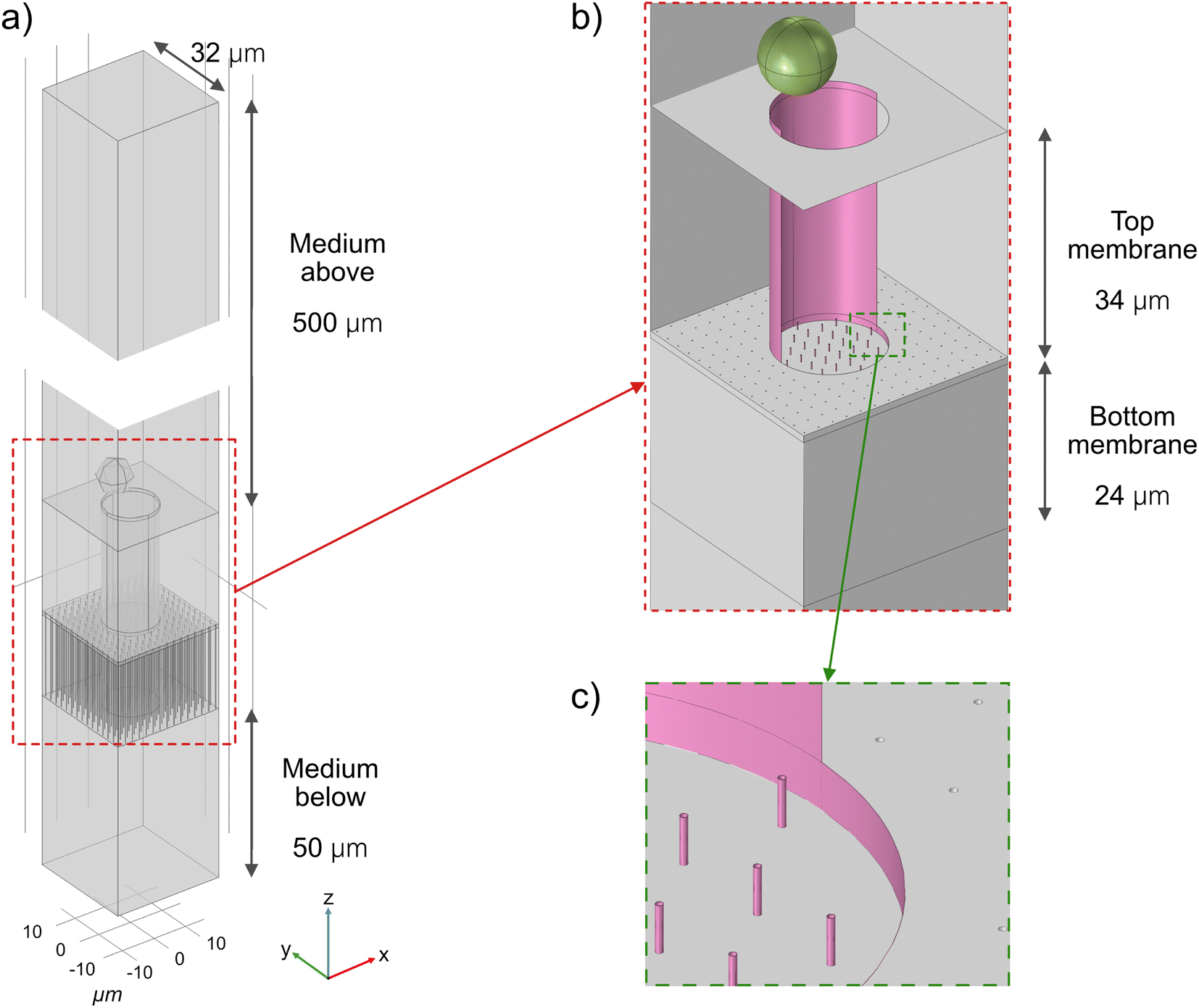 | ||
| Fig. 2 Overview of the finite element model. (a) The simulated geometry, from top to bottom, includes: a 500 μm thick layer of medium containing the cell, the top membrane with a 15 μm diameter well, the bottom membrane with 150 nm straws (pores), and a 50 μm thin layer of medium. An AC electric field is applied between the top and the bottom of the model. (b) Close-up view of the membranes, the well, and the cell. The top membrane and some of the walls of the microwell have been hidden to show inner structures. (c) Close-up view of the nanostraws at the bottom of the microwell. | ||
The material properties are set according to the default value from the software (COMSOL Multiphysics) or reliable sources. The electrical properties of the cells are adapted from Chang et al.13 and can be found in Table S1.†
The simulations include two steps: static and dynamic simulation. In the first step, the Electric Current module of COMSOL is used to calculate the electric field distribution in the model with the presence of the cell. The DEP force acting on the cell can be evaluated by integrating the Maxwell stress on its surface. By varying the positions of the cell, a map of the DEP force as a function of the position is produced. In the second step, the Particle Tracing for Fluid Flow module is used to model the trajectory of the cell. The forces acting on the cell include gravity, buoyancy, Stokes' drag, and DEP force evaluated in the previous step.
Scanning electron microscopy
The samples were coated with 5 nm of Pt/Pd in a ratio of 8![[thin space (1/6-em)]](https://www.rsc.org/images/entities/char_2009.gif) :2 and imaged using a scanning electron microscope (SEM Leo, Zeiss).
:2 and imaged using a scanning electron microscope (SEM Leo, Zeiss).
Results and discussion
DEP trapping
Because the cell-sized microwells are fabricated in insulating polycarbonate, they also act as dielectric structures, give rise to a local electric field gradient with maxima located inside the microwells and act therefore as cell traps.When applying an AC field across the substrate, the following dielectrophoretic force acts on the cells:

 is the time averaged electric field (root mean square),
 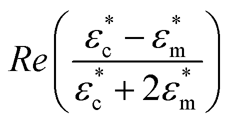 is the real part of the Clausius Mossotti factor.
  and
and  are the complex permittivities of the cell and the medium, respectively;
  , where ε is the permittivity, σ the conductivity and f the frequency.
The microwell-nanostraw device is designed so that the electric field increases in the vicinity of the wells. Therefore, in order for the dielectrophoretic force to direct the cells towards the wells (i.e. positive dielectrophoresis, a situation where the cells are attracted to regions of high electrical field), the condition  needs to be fulfilled.
We have performed simulations of the real part of the Clausius Mossotti factor for cells under various frequencies and buffer conductivities (Fig. S1†). The results suggest that positive dielectrophoresis takes place for low conductivity buffers (σ < 0.5 S m−1) and high frequencies (ν ≥ 2 MHz). We have therefore used diluted RPMI cell medium in 0.3 M D-mannitol (1/32 in volume) and used it as cell suspension buffer with a resulting conductivity of σ = 0.045 S m−1 (measured using the LAQUAtwin B-771 Conductivity Sensor S070 (HORIBA)). The presence of mannitol ensures that the cells are at osmotic equilibrium, despite being suspended in a low salt buffer. Jurkat T cells, at a concentration of ≈106 cells per mL were suspended in the low conductivity buffer and loaded in the top chamber of the microwell-nanostraw device.
An AC electric field (2.5 MHz, 50Vpp) was applied across the substrate while imaging the cells using bright field microscopy (see experimental section for detailed experimental protocol). Representative brightfield images of the substrate before and after application of the AC electric field are shown in Fig. 3, clearly showing the increase in number of wells occupied by a cell after the application of the electric field (see also Movie S1, S2†).
 | ||
| Fig. 3 Brightfield microscopy images of the microwell-nanostraw substrate before (a) and after (b) the application of the AC electric field. See Movie S2† for full sequence of events. The green arrow points at a cell and the orange arrow points at a microwell. Scale bars 50 μm. | ||
After DEP trapping (see Experimental section), 78.7% of the wells were occupied by cells (±4.7% standard deviation). The viability of the cells after DEP was assessed using the viable cell stain Calcein AM (see Experimental section and Fig. S2† for representative images of the calcein AM stained cells after DEP). The results show that 95.9% (±0.1% standard deviation) of all cells in the chamber are alive after DEP and that 99.2% (±1.4% standard deviation) of the cells located at the bottom of a well are alive after DEP.
Nanostraw-assisted injection of propidium iodide
After DEP, the low conductivity buffer was replaced by cell imaging buffer in the top chamber and the membrane impermeable nucleic acid dye propidium iodide (PI) at a concentration of 50 μg mL−1 in 0.1× PBS was loaded in the bottom chamber. Trapped cells were subjected to mild DC electrical pulses to inject PI using the nanostraws (referred to as nanostraw injection from this point). The DC pulses had an amplitude of 27.5V + 1.2 V offset, with a duration of 200 μs. The pulses were applied 3 times at 40 Hz each during 30 s with 1 minute in between each series (see experimental section for detailed experimental setup and protocol). After nanostraw injection, 29.2% (±11.8% standard deviation) of the cells located at the bottom of the wells exhibited red fluorescence, thus implying successful injection of PI (see Fig. S3† for representative images of the cells after PI injection). In order to evaluate the effects of the nanostraw EP on the cell viability, mock EP without PI was performed since the dye kills the cells once in the cytosol. Afterwards, the cells were stained with Calcein AM. The results show that 90.3% (±13.4% standard deviation) of the cells at the bottom of the wells were alive after DEP followed by mock nanostraw injection (see Fig. S4† for representative images of the cells stained for Calcein AM after DEP and mock injection). A summary of the cell viability at the different stages of the experiment can be seen in Fig. 4. | ||
| Fig. 4 Cell viability and standard deviation assessed at different timepoints of the experiment: % of live cells before loading the cells in the device (assessed using Trypan Blue), % of live cells among cells located at the bottom of the wells (using Calcein AM), % of live cells among all cells visible in the device after DEP (assessed using Calcein AM) and % of live cells among cells at the bottom of the wells after DEP and mock EP (assessed using Calcein AM). No statistically significant difference between the groups was found using 1-way Annova. | ||
Modelling
Vectors representing the DEP force acting on a cell are shown in Fig. 5. Since the geometry is cylindrical, only variations in the x and z-positions of the cell need to be considered. The red dotted lines outline the well and the green dotted lines show the border between the top and the bottom membrane. The simulations show that the cell is attracted into the well due to positive DEP. Inside the well, the cell is attracted to the center of the well (x = 0) and stabilizes in z at a position located approximately one third of the well depth away from the top of the well.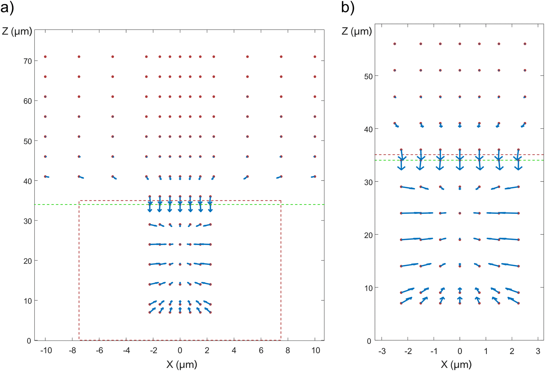 | ||
| Fig. 5 DEP force map, based on Maxwell stress (based on experimental conditions corresponding to 50 Vpp, 2.5 MHz). The red dots represent the possible positions of the center of mass of the cells, the vectors represent the directions and the magnitude of the DEP force (log scale). See Fig. 2a for the orientation of the coordinate axis with respect to the device. (a) DEP force map inside the well and above the top membrane. The outline of the well is denoted by the red dotted lines, whereas the border between the top membrane and the medium above it is denoted by the green dotted line. Note that since the cell diameter is two thirds of the well diameter, its center of mass can only be located within a cylinder whose diameter is one third of the well diameter. (b) Close-up view of the DEP force map inside the well. | ||
In order to get a more precise description of the cell trajectory in the device, dynamic simulations were performed, where gravity, buoyancy, Stokes' drag, and DEP force were accounted for. From these dynamic simulations, the trajectory of the cell can be plotted as a function of time (Fig. 6). See also ESI Movies S3 and S4.† It takes approximately 176 seconds for the cell to settle from a height of 500 μm above the top membrane to the opening of the well (as opposed to 182 seconds in the case the electrical force is absent (Movie S5†)). At a height of around 60 μm, the DEP force starts to dominate over buoyancy and drags the cell into the well (Fig. 6b). Inside the well, as z decreases, the DEP force becomes smaller and the cell stabilizes where the sum of forces is 0. The field is turned off at 180 s, after which the cell settles down and finally rests on top of the nanostraws (Fig. 6c). See also ESI Movies S3 and S4.†
 | ||
| Fig. 6 Trajectories of a cell in a simulated experiment where the cell settles from 500 μm above the top membrane in medium. (a) Whole trajectory. The field is turned off at 180 s. (b) The cell floats at a balanced position before the field is turned off. (c) After the field is off, the cell continues to settle down and finally rests on the nanostraws. | ||
Discussion
In this paper, we show that DEP can be used to direct T cells to microwells before they can be interfaced with nanostraws. The use of DEP enables precise positioning of cells in wells with nanostraws at the bottom. This results in a high coverage of the nanostraw surface, which is a prerequisite to minimizing the voltage drop across the nanostraw substrate during transfection. Indeed, in previous studies performed on flat nanostraw substrates with optimized Jurkat T cell densities, the protocol states that 0.2 × 10⁶ cells are spun down on nanostraws located at the bottom of a tube of inner radius rtube = 3 mm.5,17The corresponding cell density on the surface is therefore.

NScovered = cell density × cell area = 7.07 × 10⁹ × π(575 × 10−6)2 = 73%, assuming a single layer of cells and an average radius of 5.75 μm for Jurkat T cells.18
In the present case:
Without cells, the percentage of covered nanostraws is:
| NScovered = 1 − (well density × well area) = 82.3% |
We therefore have a smaller proportion of void nanostraws with the present method than when using flat nanostraw substrates with an optimized cell surface density. Moreover, one benefit of our method is that this higher coverage of nanostraws is achieved with a cell density on the substrate equal to
| (well density × well occupation rate × cell area) = 7.87 × 10⁸ cells per m2, |
When fewer cells are available, concentrating cells before interfacing them with a flat nanostraw substrate could seem like a simpler option. The simplest method to concentrate cells is centrifugation. However, when the number of cells is low, centrifugation does not work, as a substantial part of the cells are rinsed away with the supernatant. Therefore, one would need to use more advanced techniques to concentrate cells, such as acoustophoresis19 or deterministic lateral displacement.20 Using one of these methods would result in added complexity and require another microfluidic device upstream of the nanostraw substrate. Another possibility would be to reduce the area of the flat nanostraw substrate in order to maximize cell surface-density. However, there is a limit to how small tubes can be used when using nanostraws. The 6 mm inner diameter tubes used in studies5,17 are probably on the lower limit, as one needs to have enough space to insert electrodes and to pipette cells inside the tube. Therefore, we believe that the present method is one possible additional method aiming at minimizing the number of void nanostraws on the surface when handling cells in small amounts/concentrations.
Further minimizing the proportion of void nanostraws could be achieved by increasing the well occupancy rate, which was measured to be 78,7%. The cells need to be within the DEP force field of the well in order to be attracted to the well. From our simulations (Fig. 6), in the z direction, cells need to be within approximately 60 μm above the nanostraw substrate to be directed to the well. Therefore, cells need to first sediment to this height before being affected by the DEP force field. In the xyz plane, our simulations show that cells sedimenting from any xyz location within the geometrical unit-cell are eventually attracted to the center of a well. The dimensions of this unit cell are such that on average, the well density is the same as the one we used (105 microwells per cm2). However, in reality, the spatial distribution of the wells is random and there can possibly be regions where the distance between two wells is too large for the DEP force field to reach these regions. This can lead to a higher number of untrapped cells and therefore indirectly to a lower well occupation-rate. To increase the well occupation rate, stirring the remaining untrapped cells could move them to a DEP force field and eventually to the center of a well.
A possible drawback of our method lies in the difficulty to retrieve the treated cells from the wells using simple pipetting after nanostraw injection, in contrast to what is done routinely on flat nanostraw substrates. This issue can be addressed using trypsin to detach the cells from the wells.
Another drawback of the method is the requirement of low conductivity buffer in order to use DEP, which leads to one extra medium exchange, and which may affect the cell viability in the long term. However, with our experimental setup, one has direct access to the top and bottom chambers and exchanging the medium is easy. Moreover, our results show that the cell viability is not affected by the process, at least on the timescale of our experiments.
In our case, ≈30% of the cells were efficiently injected with PI. This relatively low efficiency may be explained by the fact that, in general, non-adherent cells are more difficult to transfect compared to adherent cells.21,22 To our knowledge, the only studies using nanostraws to transfect Jurkat T cells used a commercially available nanostraw equipment delivering square waves at 400 Hz for 2 min (ref. 5 and 17) (the “Navan 100 box” from NAVAN Technologies, Inc., San Carlos, CA). The design of the setup being unknown, this makes it difficult to compare our results. In another study22 where nanopores instead of nanostraws are used to transfect Jurkat T cells via electrical pulses, the transfection efficiency varies between ≈10% and 75%, depending on the voltage applied to the electrodes. There too, it is difficult to compare results, as the distance between electrodes is not mentioned and therefore the electric field cannot be estimated. In that study, the transfection efficiency is lower for Jurkat cells compared to adherent cells and the reason for this is thought to be a larger gap between the cell membrane and nanopore.22 This gap may be reduced by centrifugating the cells on the nanopores and/or functionalizing the surface with adhesion-promoting molecules.
In our case, it might be possible to improve the injection efficiency by varying the voltage, by functionalizing the surface with adhesion-promoting molecules or by centrifuging the cells after DEP trapping.
Another way to increase the injection efficiency could be to ensure that the DEP maximum force is located at or below the nanostraw substrate in order to “press” down the cells onto the nanostraws. This could possibly be achieved by using a more conductive polymer for the nanostraw and associated membrane material and sandwiching the nanostraw substrate between two dielectric polymers forming wells that continuously decrease in diameter towards the nanostraws, with a minimum diameter just below the nanostraws. Note that increasing the injection efficiency is beyond the scope of the present paper as the main focus is the demonstration of the use of DEP for manipulating cells in order to bring them in contact with nanostraws and not the nanostraw injection efficiency per se.
Whereas previous studies using nanostraws have used centrifugation or magnetic forces to direct cells to nanostraws,3,5,17,23 the present method offers an alternative method to direct cells towards the substrate, not requiring any centrifugation step, cell concentration or cell modification. The method can be useful when fewer cells are available to work with, such as when working with circulating tumor cells and antigen specific T cells, for example.
Conclusions
In conclusion we show both with simulations and experiments that positive DEP can be used to direct cells on a substrate to specific microwells with nanostraws at the bottom without using centrifugation. The nanostraws are subsequently used to deliver PI to the cells using mild electrical pulses. Directing cells to the wells leads to a minimization of the number of uncovered nanostraws, and therefore ensures that most of the voltage drop occurs across the cells, which is important for delivering cargos inside cells. The whole process does not have any measured negative effect on the cell viability. In the future, this method may be of great help when working with transfecting rare cells, especially when the nanostraw substrate cannot be entirely covered by cells due to the low number of cells.Conflicts of interest
The authors have no conflict of interest.Acknowledgements
This work was financed by the ERC-CoG-grant NanoPokers (grant agreement no. 682206), NanoLund, the Crafoord Foundation, MyFab (nanofabrication at Lund Nano Lab), the Swedish Research Council (VR) and the Swedish Foundation for Strategic Research (SSF).References
- J. J. VanDersarl, A. M. Xu and N. A. Melosh, Nano Lett., 2012, 12, 3881–3886 CrossRef PubMed.
- X. Xie, A. M. Xu, S. Leal-Ortiz, Y. Cao, C. C. Garner and N. A. Melosh, ACS Nano, 2013, 7, 4351–4358 CrossRef PubMed.
- L. Schmiderer, A. Subramaniam, K. Žemaitis, A. Bäckström, D. Yudovich, S. Soboleva, R. Galeev, C. N. Prinz, J. Larsson and M. Hjort, Proc. Natl. Acad. Sci. U. S. A., 2020, 117, 21267–21273 CrossRef PubMed.
- E. Hebisch, M. Hjort, D. Volpati and C. N. Prinz, Small, 2021, 17, 2006421 CrossRef PubMed.
- A. Tay and N. Melosh, Adv. Ther., 2019, 1900133 CrossRef.
- Y. Cao, H. Chen, R. Qiu, M. Hanna, E. Ma, M. Hjort, A. Zhang, R. S. Lewis, J. C. Wu and N. A. Melosh, Sci. Adv., 2018, 4, eaat8131 CrossRef PubMed.
- P. Mukherjee, S. S. P. Nathamgari, J. A. Kessler and H. D. Espinosa, ACS Nano, 2018, 12, 12118–12128 CrossRef PubMed.
- H. Morgan and N. G. Green, AC electrokinetics: colloids and nanoparticles, 2002, vol. 2 Search PubMed.
- R. Pethig, Dielectrophoresis: Theory, Methodology and Biological Applications, Wiley, 2017 Search PubMed.
- C. F. Chou, J. O. Tegenfeldt, O. Bakajin, S. S. Chan, E. C. Cox, N. Darnton, T. Duke and R. H. Austin, Biophys. J., 2002, 83, 2170–2179 CrossRef PubMed.
- C. Prinz, J. O. Tegenfeldt, R. H. Austin, E. C. Cox and J. C. Sturm, Lab Chip, 2002, 2, 207–212 RSC.
- R. S. Thomas, H. Morgan and N. G. Green, Lab Chip, 2009, 9, 1534–1540 RSC.
- L. Chang, D. Gallego-Perez, X. Zhao, P. Bertani, Z. Yang, C. L. Chiang, V. Malkoc, J. Shi, C. K. Sen, L. Odonnell, J. Yu, W. Lu and L. J. Lee, Lab Chip, 2015, 15, 3147–3153 RSC.
- R. T. Abraham and A. Weiss, Nat. Rev. Immunol., 2004, 4, 301–308 CrossRef CAS PubMed.
- Y. Huang and R. L. Wange, J. Biol. Chem., 2004, 279 Search PubMed.
- J. Fang, J. Xu, Y. Xiang, H. Li, D. Xu, X. Xie and N. Hu, Biosens. Bioelectron., 2021, 194 DOI:10.1016/j.bios.2021.113583.
- A. Tay and N. Melosh, Small, 2021, 17, 2103198 CrossRef CAS PubMed.
- M. J. Rosenbluth, W. A. Lam and D. A. Fletcher, Biophys. J., 2006, 90, 2994–3003 CrossRef CAS PubMed.
- T. Laurell, F. Petersson and A. Nilsson, Chem. Soc. Rev., 2007, 36, 492–506 RSC.
- J. P. Beech, S. H. Holm, K. Adolfsson and J. O. Tegenfeldt, Lab Chip, 2012, 12, 1048 RSC.
- S. Basiouni, H. Fuhrmann and J. Schumann, Biotechniques, 2012, 53, 1–4 CrossRef PubMed.
- Y. Cao, E. Ma, S. Cestellos-Blanco, B. Zhang, R. Qiu, Y. Su, J. A. Doudna and P. Yang, Proc. Natl. Acad. Sci. U. S. A., 2019, 116, 7899–7904 CrossRef CAS.
- M. A. Pop and B. D. Almquist, Adv. NanoBiomed Res., 2021, 1, 2000061 CrossRef PubMed.
Footnote |
| † Electronic supplementary information (ESI) available. See DOI: https://doi.org/10.1039/d2ra05119b |
| This journal is © The Royal Society of Chemistry 2022 |