
 Open Access Article
 This Open Access Article is licensed under a Creative Commons Attribution-Non Commercial 3.0 Unported Licence
Photo-enhanced growth of lead halide perovskite crystals and their electro-optical properties†
Shiwei Wang *ab,
Yixuan Wanga,
Qi Weia and
Junling Wang*c
*ab,
Yixuan Wanga,
Qi Weia and
Junling Wang*c
aSchool of Chemical Engineering, Advanced Research Institute of Materials Science, Changchun University of Technology, Changchun, 130012, China. E-mail: wswjldx2004@163.com
bHainan Vocational University of Science and Technology, Haikou, 571126, China
cSchool of Physics, Southern University of Science and Technology, Shenzhen, 518055, China. E-mail: jwang@sustech.edu.cn
First published on 29th September 2022
Abstract
Organic–inorganic hybrid perovskites have attracted much attention for opto-electronic applications due to their low trap density, strong light absorption, and superior charge transport performance. Generally, the high efficiency of perovskite electro-optical thin films depends on their high-quality perovskite single crystals. In this work, the external illumination is applied on the perovskite single crystals growing in solution. It was shown that larger size CH3NH3PbI3 single crystals can be obtained under illumination conditions. In addition, CH3NH3PbI3 films are prepared by a one-step spin coating process under illumination, the crystal size and film quality of which have been obviously improved due to the effect of illumination in the film forming process. The efficiency of the average cells based on CH3NH3PbI3 films increased from 15.2% for the normal conditions to 17.7% for the illumination one, which is consistent with the light enhanced growth of CH3NH3PbI3 single crystals in their solution. The “photo-inhibition nucleation” mechanism is proposed to explain the light-induced enhancement of perovskite crystal growth.
1. Introduction
Organic–inorganic hybrid perovskites (OIHP) have attracted much attention for solar cells and optoelectronic applications due to their low trap density, strong light absorption, and superior charge transport performance.1–4 The photoelectric conversion efficiency (PCE) of OIHP-based solar cells has reached more than 24.2% quickly after a short period of development.5 Several methods have been used to improve the performance of perovskite solar cells, such as synthesis of novel electronic transmission materials,6,7 hole transport materials,8 different types of perovskite materials and device structures.9 However, the type and quality of perovskite crystals is the fundamental source of high efficiency photovoltaic cells.10 So, the growth of perovskite crystals and their development of electro-optic applications have always been an important subject.11 Certainly, it is one of the important ways to improve the PCE of perovskite solar cells by improving the quality of perovskite polycrystalline thin films.12The relationship between light, perovskite material, and device performance is a key topic that researchers pay close attention to.13–15 They have always focused on the research of the response characteristics of the device to light.16 The light response during single crystal growth is seldom noticed. Methylazanium iodide perovskite (MAPbI3) materials have been widely studied in solar cells due to its light absorption and band gap properties, and the study of its physical properties and growth process is often carried out as a typical representative of OIHP materials.17,18
In this work, MAPbI3 single crystals are prepared by solution precipitation. During single crystal growth, a white light source is applied to light from outside. During the growth of perovskite single crystals in solution, it is found that continuous external light can promote the growth of large-sized single crystals. On this basis, MAPbI3 films are prepared by one-step spin coating process under illumination, the crystal size and film quality of which have been obviously improved because of illumination in the film forming process. Therefore, the photoelectrical properties of MAPbI3 single crystals and films grown under light conditions are greatly improved.
2. Method
2.1 Preparation of MAPbI3 single crystals
PbI2 (5.5 g, 99.99%, Sigma-Aldrich) and CH3NH3I (2.0 g, 99.9%, Sigma-Aldrich) was mixed in γ-butyrolactone (GBL, 10.0 mL, AR ≥99%, Sigma-Aldrich), then the growth solution would be achieved by sealing the mixed solution in a glass bottle with stirring at 60 °C for 1 h under dark. The glass bottle with a growth solution was left in the oven at 100 °C under illumination for a certain time. All the operations were carried out under dark condition except the special light source used in the experiment. MAPbI3 single crystals with different sizes can be obtained by controlling the light intensity and illumination time on the precursor solution.2.2 Device fabrication
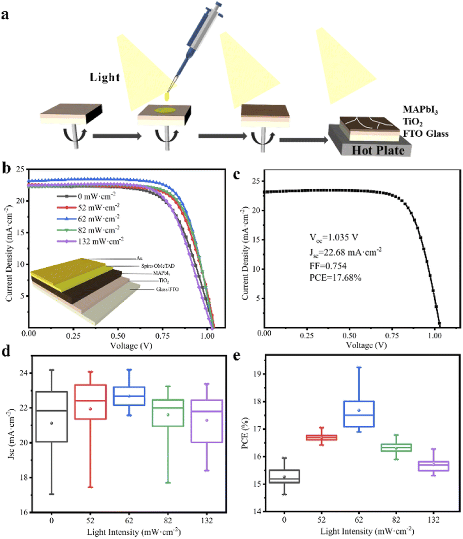
To study the dependence of the device performance on illumination conditions, the perovskite absorbing layer was prepared under illumination with different intensity in nitrogen-filled glove box (40% of MAPbI3 in GBL) by spin coating at 5000 rpm for at least 60 s, chlorobenzene was added after 30 seconds. Then annealed at 100 °C for 1 hour. (Note that perovskite layer remains in the light during spin-coating and annealing). Spiro-OMeTAD/chlorobenzene (72.3 mg mL−1) solution was employed with the addition of 17.5 μL of Li-TFSI/acetonitrile (520 mg mL−1), and 28.8 μL of 4-tert-butyl pyridine. 30 μL of Spiro-OMeTAD solution mixed above was spin-coated on the perovskite film at 3000 rpm for 30 s, where finally, a gold layer with a thickness of 100 nm was deposited as the counter electrode on the top of Spiro-OMeTAD layer through shadow masks via thermal evaporation under high vacuum (5 × 10⁻⁵ Torr). The perovskite single crystal device can be obtained by evaporating gold electrode on the larger plane of the perovskite crystal.2.3 Measurements
Keithley 2400 source meter was used to record the photocurrent response signal under 20 V bias voltage with a light intensity of 100 mW cm−2. The spectral photo response measurements were performed with a 150 W halogen lamp equipped with a manual monochromator. Optical power meter (SM206-SOLAR solar power meter) was used to measure the incident powers. J–V curves of the PSCs were measured using a Keithley 2400 source under ambient conditions at room temperature. The light source was a 450 W xenon lamp (Oriel solar simulator) with a Schott K113 Tempax sunlight filter (Praezisions Glas & Optik GmbH) to match AM1.5G. The light intensity was 100 mW cm−2 calibrated by an NREL-traceable KG5-filtered silicon reference cell. All measurements were taken at room temperature. UV-vis absorption spectra were recorded using Agilent Cary 5000 at room temperature in the absorption mode and the fluorescence spectra were obtained using the PerkinElmer LS55 fluorescence spectrometer with the excitation wavelength of 365 nm. To reduce the sample variance, at least three samples were determined for each group and the average of all spectra presented. X-ray diffraction data were collected on a high-resolution diffractometer by Rikagu Smart lab (Cu-Ka radiation). SEM measurements were carried out in a scanning electron microscope (JSM-7610Fplus, JEOL).3. Results and discussion
MAPbI3 single crystals are grown from their precursor solutions by the inverse temperature crystallization method at 100 °C, both in dark and under light illumination.19,20 The differences in crystal size and number can be obviously observed in the eye for the MAPbI3 single crystals grown with and without illumination. As shown in Fig. 1a, under illumination condition, MAPbI3 single crystals with small quantity but large size are obtained in the solution. However, the number of MAPbI3 single crystals grown in the dark is large but the size is small. Besides, different intensities of light are used to grow their single crystals, which can be found that the largest size for MAPbI3 single crystals were got under the light intensity of 62 mW cm−2 (Fig. S1†). The structure of MAPbI3 crystals was characterized by X-ray diffraction (XRD), which characteristic peaks are in good agreement with literature reported (Fig. 1b and S2†).20,21 It can be confirmed that the structure of perovskite single crystal is not affected by light exposure during growth. By comparing the growth of MAPbI3 single crystals under light (62 mW cm−2) and in dark, as shown in Fig. 1c and d, it is clearly seen from the statistical results that the number of crystals obtained under illumination is less than that in dark. However, the size of the crystals is obvious larger.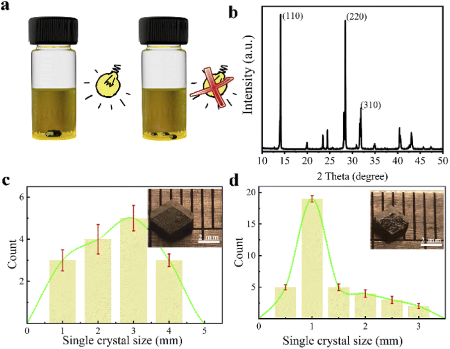 | ||
| Fig. 1 (a) Growth processes of MAPbI3 crystals under light and dark conditions, the light intensity of which is 64 mW cm−2. (b) XRD curves for MAPbI3 single crystal. And the statistical data of the size and number of MAPbI3 single crystals in their precursor solutions under light (c) and dark (d) conditions, respectively. The insert images are the MAPbI3 single crystal grown from its precursor solution after 36 h. | ||
In order to exclude the effect of temperature change due to illumination on the growth of MAPbI3 single crystals, infrared thermometer has been used to track the temperature of the precursor solution. The results show that the temperature fluctuation is less than 0.3 °C, regardless of whether it is in dark or under light (Fig. S3†). It is unlikely that such a small change in the precursor solution temperature will have such a large effect on the growth of MAPbI3 single crystals.
The photo-inhibition of nucleation theory was proposed to explain the perovskite crystals enhanced grown under illumination. UV-vis absorbance spectrum of MAPbI3 precursor solutions has been detected to investigate the crystal grown process. As shown in Fig. 2a–c, there are a large number of complexes in the MAPbI3 precursor solution, such as PbI42− and PbI3−.22 With the solution temperature increasing, the lead halide complexes are dissolved due to the H+ produced from butyrolactone. Then, MAPbI3 crystal nucleus will precipitate due to more free ions formed from the super-saturation of PbIn(n−2)− complexes in solutions.23,24 As shown in Fig. 2a and b, the absorption peaks at 325 nm and 375 nm are attributed to PbI42− and PbI3− complexes in the solution, respectively.22,25,26 The strength of these absorption peaks are decreased with the increase of the growth time. However, the absorption peaks decrease more significantly in the initial stage of crystal growth in dark than those under illumination (Fig. 2c). It suggests that the nucleus is easier to be formed when perovskite single crystal's growth is carried out in dark conditions. So more MAPbI3 nucleus are precipitated from the solution in dark, which are used to grow for MAPbI3 single crystals. On the contrary, less MAPbI3 nucleus are precipitated from the solution under illumination, so the number of MAPbI3 crystals grown in dark is obvious larger than the ones under light. PbIn(n−2)− colloids in the solution will gradually break down into free ions for the growth of MAPbI3 single crystals. In the same initial precursor solution, the size of MAPbI3 single crystals will be larger under illumination than the one under dark due to more free ions in the solution. Note that there is a certain limit to the formation and decomposition of PbIn(n−2)− colloids, that is, the photoinhibition nucleation effect is also within a certain limit, not infinite, therefore, the appropriate light intensity (64 mW cm−2) can grow the largest single crystal.
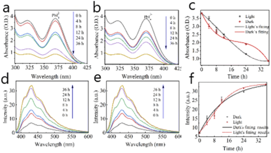 | ||
| Fig. 2 (a and b) UV-vis spectra of MAPbI3 precursor solutions with different single crystal growth times under light and dark conditions, respectively. (c) Fitted curves of the absorbance peak at 375 nm. PL spectra of MAPbI3 precursor solution with different growth times of single crystals under light (d) and dark (e) conditions. (f) Fit curves of the photoluminescence peak at 431 nm. | ||
The fluorescence spectrum of precursor solutions is also used to confirm the “photo-inhibition nucleation theory” further. It can be seen from Fig. 2d–f that the intensity of the photoluminescence peak is increasing with the increase of the growing time of MAPbI3 single crystals, which is attributed to the decrease of iodine ions in solution.27 The fluorescence characteristic here is attributed to the iodine ion in the solution, which is dissociated from a variety of lead iodide colloids, so it is a trend towards relative equilibrium. However, the increase of absorption peak under dark conditions is more obvious, which shows that the amount of iodine ions in dark is less than the one in light conditions (at least 0–14 h). While the crystal in the solution is just at the nucleation stage, so it can be inferred that light can inhibit the nucleation process of MAPbI3 crystal by affecting the decomposition of PbIn(n−2)− complexes in the solution. So “photo-inhibition nucleation theory” is proposed to explain the phenomenon of light-induced single crystal growth.
Perovskite films are formed from the process of single crystal precipitation and solvent volatilization. Polycrystals in perovskite films are also formed by nucleation and growth processes, which is similar to the process of saturated precipitation of perovskite single crystals. The photo-enhanced perovskite single crystal may be suitable for perovskite polycrystalline thin films. According to the “photo-inhibition nucleation theory” for the growth of MAPbI3 crystals proposed above, MAPbI3 films have been prepared by one-step spin coating process under illumination and their solar cells based on them was also constructed. As shown in Fig. 3, the average size of MAPbI3 crystals in the thin films can be obviously observed from the SEM photos of the thin films prepared under dark and light. It can be clearly revealed that the grain size of MAPbI3 in the film obtained under illumination of 62 mW cm−2 of white light is obviously larger than that in dark. The statistics of crystal size in thin films are shown in Fig. 3, the laws and trends of which are exactly the same as that for MAPbI3 single crystal growth.
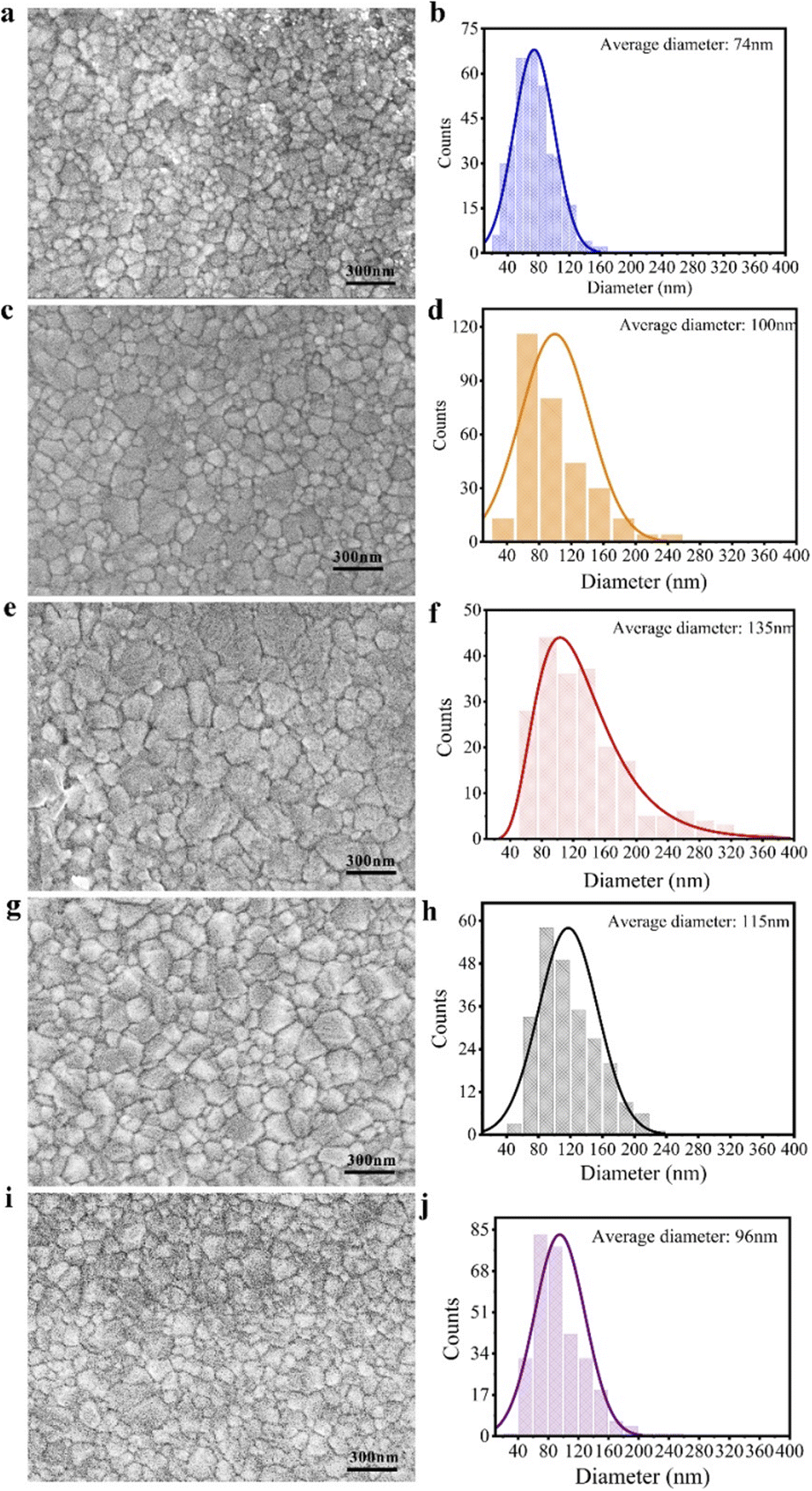 | ||
| Fig. 3 SEM images of MAPbI3 films obtained by spin-coating under different illumination intensities ((a) 0 mW cm−2, (c) 52 mW cm−2, (e) 52 mW cm−2, (g) 82 mW cm−2, (i) 132 mW cm−2). The statistics of the grain diameter distribution of the MAPbI3 microcrystalline in films ((b, d, f, h and j) is corresponding to the sample of (a, c, e, g and i), respectively). | ||
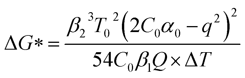
Besides, MAPbI3 polycrystalline films are prepared by one-step spin-coating on the interdigital electrodes under illumination. As shown in Fig. 4, a large photocurrent can be detected when a beam of light illuminates on the surface of the film. In addition, when the light with the intensity of 62 mW cm−2 is introduced during the film spin-coating process, the obtained MAPbI3 film shows the highest current value and on/off ratio, which is attributed to the large crystal size and dense stacking structure in the film.28 Perovskite devices based on FTO/TiO2/MAPbI3/Spiro-OMeTAD/Au structure are also constructed, the photoelectric transformation efficiencies of which were detected from their J–V curves. As shown in Fig. 5, the average PCE of the devices is the highest at 17.7%, when their MAPbI3 films were prepared under the illumination of 62 mW cm−2 light intensity. It can be confirmed that the high PCE of perovskite device was attributed to its morphology of thin films with compact accumulation of bulk crystals under illumination. In another, it can be observed from Fig. 5c that the short circuit current density (JSC) of the device is greatly affected by the morphology of MAPbI3 thin films. When the thin film devices prepared under illumination, not only the value of their JSC is increased, but also the distribution of JSC for the 18 devices is more concentrated. In a word, when the perovskite thin film is prepared under illumination, the efficiency of their cells will be higher and the reliability will be better. Through this work, it can be proposed to introduce the illumination into the preparation and production of perovskite thin-film solar cells. It is worth emphasizing that the highest efficiency of perovskite cells is not the goal, but the repeatability of the experimental results of multiple device samples can prove the idea of this work.
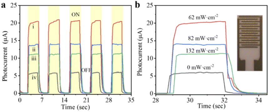 | ||
| Fig. 4 (a) Photoelectric response for MAPbI3 films fabricated on interdigital electrode under illumination (1 sun of light intensity and the electrode spacing is 0.14 mm); (b) the enlarged curves for (a) and the intensity of illumination for MAPbI3 films constructed have been signed-in the curves. | ||
 | ||
| Fig. 5 (a) Scheme for the preparation process of MAPbI3 films under illumination. (b) J–V curves for the cells based on MAPbI3 obtained under different intensities of light, the inset of which is the device structure. (c) J–V curve and PCE for the cells prepared under illumination with the light intensity of 62 mW cm−2. (d and e) Is the statistical data of the JSC and PCE for the cells (area is 0.09 cm2). | ||
In addition, the thermodynamic critical factor in nucleation is the critical free energy of nucleation (ΔG) and the critical nucleus size (rk), which can be described with the following (eqn (1) and (2)) (ESI Note 1†):29–32
 | (1) |
 | (2) |
According to the nucleation kinetics, a stable crystal nucleus can only be formed when their size is larger than the critical nucleus size.32 According to the “photoinhibition nucleation Theory” and photochemical reaction, there will be less free ions in the solution for the formation of nucleation when the perovskite precursor solution is placed under light.33–38 At the same time, the migration rate of free ions in solution will be increased due to the effect of light outside.33–38 So, the charge density on the crystal nucleus surface will be less under the light. According to the equations mentioned above (eqn (1) and (2)), the critical free energy of nucleation (ΔG*) and the critical nucleus size (rk) will be increased under light 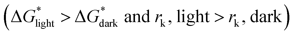 . Thus, the crystal nucleus is more difficult to have existed in stable and grown-up under light than the ones under dark.
After the formation of MAPbI3 crystal nuclei under light or dark, MAPbI3 nuclei will continue to grow in the precursor solution to form single crystals. Surprisingly, when other conditions are consistent, the size of MAPbI3 single crystals grown under light conditions in the solution is obviously larger than the ones under dark, which can be seen from Fig. 1. This was largely due to the vibration frequency of the atom in the solution will be increased because of appropriate light outside.39,40 And the driving force of crystal growth under light is larger than under dark (Δgv, light > Δgv, dark) (it is obtained by eqn (1)). In addition, the electrostatic interaction on the crystal surface caused by the illumination can also accelerate the deposition of free ions and promote the growth of the MAPbI3 crystals.
4. Conclusions
In summary, a photo-enhanced effect on the growth process of MAPbI3 crystals have been investigated in this work. It can be confirmed that the perovskite crystals can be grown more larger under external illumination. “Photo-inhibition nucleation theory” is proposed preliminarily to explain the dynamic mechanism. It can be inferred that appropriate external illumination can inhibit the formation of perovskite crystal nuclei in the precursor solution but facilitate the growth of the single crystals. The growth law of perovskite single crystal can be directly applied in the preparation process of their thin films. So, the photo responses for MAPbI3 films constructed by one-step spin coating under illumination are obviously enhanced. Depending on the large single crystal size and dense packing film morphology, the efficiency of MAPbI3 solar cells constructed based on the illumination MAPbI3 films are obviously improved compared with the normal devices, the reliability of which can be proved through repeated experiments. This work provides a new method for improving the efficiency of perovskite solar cells, and provides a direction for perovskite research.Conflicts of interest
There are no conflicts to declare.Acknowledgements
The authors gratefully acknowledge the funding of this research by the National Natural Science Foundation of China (Grant no. 21204087); the Changchun Science and Technology Development Plan Project (21ZY39); Jilin Innovation and Entrepreneurship Talent Project (2021Y002); Jilin Science and Technology Development Project (YDZJ202201ZYTS557, 20220508154RC, 20200403142SF and 20210203111SF).References
- J. P. Correa-Baena, M. Saliba, T. Buonassisi, M. Gratzel, A. Abate, W. Tress and A. Hagfeldt, Promises and challenges of perovskite solar cells, Science, 2017, 358, 739–744 CrossRef CAS PubMed
.
- A. K. Jena, A. Kulkarni and T. Miyasaka, Halide Perovskite Photovoltaics: Background, Status, and Future Prospects, Chem. Rev., 2019, 119, 3036–3103 CrossRef CAS PubMed
- K. Y. Wang, G. C. Xing, Q. H. Song and S. M. Xiao, Micro- and Nanostructured Lead Halide Perovskites: From Materials to Integrations and Devices, Adv. Mater., 2021, 33, 2000306 CrossRef CAS PubMed
- D. Yang, R. Yang, S. Priya and S. Liu, Recent Advances in Flexible Perovskite Solar Cells: Fabrication and Applications, Angew. Chem., Int. Ed., 2019, 58, 4466–4483 CrossRef CAS PubMed
- https://www.nrel.gov/pv/cell-efficiency.html.
- Y.-Y. Zhou, H. Sternlicht and N. P. Padture, Transmission Electron Microscopy of Halide Perovskite Materials and Devices, Joule, 2019, 3, 641–661 CrossRef CAS
- S. Ravishankar, S. Gharibzadeh, C. Roldán-Carmona, G. Grancini, Y. Lee and M. Ralaiarisoa, Influence of Charge Transport Layers on Open-Circuit Voltage and Hysteresis in Perovskite Solar Cells, Joule, 2018, 2, 788–798 CrossRef CAS
- G. W. Kim, H. Choi, M. Kim, J. Lee, S. Y. Son and T. Park, Hole Transport Materials in Conventional Structural (n-i-p) Perovskite Solar Cells: From Past to the Future, Adv. Energy Mater., 2020, 10, 1903403 CrossRef CAS
- P. Schulz, D. Cahen and A. Kahn, Halide Perovskites: Is It All about the Interfaces?, Chem. Rev., 2019, 119, 3349–3417 CrossRef CAS
- J. W. Lee, D. K. Lee, D. N. Jeong and N. G. Park, Control of Crystal Growth toward Scalable Fabrication of Perovskite Solar Cells, Adv. Funct. Mater., 2019, 29, 1807047 CrossRef CAS
- C. Liu, Y.-B. Cheng and Z.-Y. Ge, Understanding of perovskite crystal growth and film formation in scalable deposition processes, Chem. Soc. Rev., 2020, 49, 1653–1687 RSC
- M. A. Haque, J. Troughton and D. Baran, Processing-Performance Evolution of Perovskite Solar Cells: From Large Grain Polycrystalline Films to Single Crystals, Adv. Energy Mater., 2020, 10, 1902762 CrossRef CAS
- H.-Q. Cao, J.-Z. Li, Z. Dong, J. Su, J.-J. Chang, Q. Zhao, Z.-Y. Li, L.-Y. Yang and S.-G. Yin, Reducing Defects in Perovskite Solar Cells with White Light Illumination-Assisted Synthesis, ACS Energy Lett., 2019, 4, 2821–2829 CrossRef CAS
- W. Tress, K. Domanski, B. Carlsen, A. Agarwalla, E. A. Alharbi, M. Graetzel and A. Hagfeldt, Performance of perovskite solar cells under simulated temperature-illumination real-world operating conditions, Nat. Energy, 2019, 4, 568–574 CrossRef CAS
- F. Zheng, W.-J. Chen, T.-L. Bu, K. P. Ghiggino, F.-Z. Huang, Y.-B. Cheng, P. Tapping, T. W. Kee, B.-H. Jia and X.-M. Wen, Triggering the Passivation Effect of Potassium Doping in Mixed-Cation Mixed-Halide Perovskite by Light Illumination, Adv. Energy Mater., 2019, 9, 1901016 CrossRef
- Y.-B. Yuan and J.-S. Huang, Ion Migration in Organometal Trihalide Perovskite and Its Impact on Photovoltaic Efficiency and Stability, Acc. Chem. Res., 2016, 49, 286–293 CrossRef CAS PubMed
- J. Haruyama, K. Sodeyama, L. Y. Han and Y. Tateyama, Surface Properties of CH3NH3PbI3 for Perovskite Solar Cells, Acc. Chem. Res., 2016, 49, 554–561 CrossRef CAS
- S.-N. Yun, X. Zhou, J. Even and A. Hagfeldt, Theoretical Treatment of CH3NH3PbI3 Perovskite Solar Cells, Angew. Chem., Int. Ed., 2017, 56(18), 15806–15817 CrossRef CAS PubMed
- B. Li, Y. Kawakita, Y. Liu, M. Wang, M. Matsuura and K. Shibata, Polar Rotor Scattering as Atomic-level Origin of Low Mobility and Thermal Conductivity of Perovskite CH3NH3PbI3, Nat. Commun., 2017, 8, 16086 CrossRef CAS PubMed
- Y. Zhou, L. You, S.-W. Wang, Z.-L. Ku, H.-J. Fan and J.-L. Wang, Giant Photostriction in Organic-Inorganic Lead Halide Perovskites, Nat. Commun., 2016, 7, 11193 CrossRef CAS PubMed
- Y.-C. Liu, Z. Yang, D. Cui, X.-D. Ren, J.-K. Sun, X.-J. Liu, J.-R. Zhang, Q.-B. Wei, H.-B. Fan, F.-Y. Yu, X. Zhang, C.-M. Zhao and S.-Z. Liu, Two-Inch-Sized Perovskite CH3NH3PbX3 (X = Cl, Br, I) Crystals: Growth and Characterization, Adv. Mater., 2015, 27, 5176–5183 CrossRef CAS PubMed
- B.-C. Li, F. H. Isikgor, H. Coskun and J. Y. Ouyang, The Effect of Methylammonium Iodide on the Supersaturation and Interfacial Energy of the Crystallization of Methylammonium Lead Triiodide Single Crystals, Angew. Chem., Int. Ed., 2017, 56, 16073–16076 CrossRef CAS PubMed
- J. W. Lee, D. J. Seol, A. N. Cho and N. G. Park, High-Efficiency Perovskite Solar Cells Based on the Black Polymorph of HC(NH2)2PbI3, Adv. Mater., 2014, 26, 4991–4998 CrossRef CAS PubMed
- F. Zheng, H. Takenaka, F.-G. Wang, N. Z. Koocher and A. M. Rappe, First-Principles Calculation of the Bulk Photovoltaic Effect in CH3NH3PbI3 and CH3NH3PbI3-xClx, J. Phys. Chem. Lett., 2015, 6, 31–37 CrossRef CAS PubMed
- D.-Q. Bi, L. Yang, G. Boschloo, A. Hagfeldt and E. M. J. Johansson, Effect of Different Hole Transport Materials on Recombination in CH3NH3PbI3 Perovskite-Sensitized Mesoscopic Solar Cells, J. Phys. Chem. Lett., 2013, 4, 1532–1536 CrossRef CAS PubMed
- M. Shirayama, H. Kadowaki, T. Miyadera, T. Sugita, M. Kato and M. Tamakoshi, Optical Transitions in Hybrid Perovskite Solar Cells: Ellipsometry, Density Functional Theory, and Quantum Efficiency Analyses for CH3NH3PbI3, Phys. Rev. Appl., 2016, 5, 014012 CrossRef
- L. Ma, F. Hao, C. C. Stoumpos, B. T. Phelan, M. R. Wasielewski and M. G. Kanatzidis, Carrier Diffusion Lengths of over 500 nm in Lead-Free Perovskite CH3NH3SnI3 Films, J. Am. Chem. Soc., 2016, 138, 14750–14755 CrossRef CAS PubMed
- W.-Y. Nie, H. Tsai, R. Asadpour, J. C. Blancon, A. J. Neukirch, G. Gupta, J. J. Crochet, M. Chhowalla, S. Tretiak, M. A. Alam, H. L. Wang and A. D. Mohite, High-efficiency solution-processed perovskite solar cells with millimeter-scale grains, Science, 2015, 347, 522–525 CrossRef CAS PubMed
- G. D. Botsaris, in Industrial Crystallization, ed. J. W. Mullin, Springer, Boston, 1975 Search PubMed
- P. W. V. Lorenz Ratke, Growth and Coarsening: Ostwald Ripening in Material Processing, Springer, 2002 Search PubMed
- W. Li, M. U. Rothmann, A. Liu, Z.-Y. Wang, Y.-P. Zhang, A. R. Pascoe, J. F. Lu, L.-C. Jiang, Y. Chen, F.-Z. Huang, Y. Peng, Q.-L. Bao, J. Etheridge, U. Bach and Y. B. Cheng, Phase Segregation Enhanced Ion Movement in Efficient Inorganic CsPbIBr3 Solar Cells, Adv. Energy Mater., 2017, 7, 1700946 CrossRef
- A. Ummadisingu, L. Steier, J. Y. Seo, T. Matsui, A. Abate, W. Tress and M. Grätzel, The Effect of Illumination on The Formation of Metal Halide Perovskite Films, Nature, 2017, 545, 208–212 CrossRef CAS PubMed
- R. Murai, H. Y. Yoshikawa, Y. Takahashi and M. Maruyama, Enhancement of Femtosecond Laser-induced Nucleation of Protein in a Gel Solution, Appl. Phys. Lett., 2010, 96, 3475 CrossRef
- K. Nakamura, Y. Sora, H. Y. Yoshikawa, Y. Hosokawa, R. Murai and H. Adachi, Femtosecond Laser-induced Crystallization of Protein in Gel Medium, Appl. Surf. Sci., 2007, 253, 6425–6429 CrossRef CAS
- G. B. Wu, R. Liang, M. Z. Ge, G. X. Sun, Y. Zhang and G. C. Xing, Surface Passivation Using 2D Perovskites toward Efficient and Stable Perovskite Solar Cells, Adv. Mater., 2021, 33, 2000306 CrossRef PubMed
- H. Y. Yoshikawa, R. Murai, S. Sugiyama, G. Sazaki, T. Kitatani and Y. Takahashi, Femtosecond Laser-induced Nucleation of Protein in Agarose Gel, J. Cryst. Growth, 2009, 311, 956–959 CrossRef CAS
- V. Adinolfi, O. Ouellette, M. I. Saidaminov, G. Walters, A. L. Abdelhady and O. M. Bakr, Fast and Sensitive Solution-Processed Visible-Blind Perovskite UV Photodetectors, Adv. Mater., 2016, 28, 7264–7268 CrossRef CAS
- X. Li, J. Xu, J.-C. Luan, X.-L. Yu, B. Zhang, S.-Y. Dai and J.-X. Yao, Preparation of CH3NH3PbCl3 film with a large grain size using PbI2 as Pb source and its application in photodetector, Mater. Lett., 2018, 220, 108–111 CrossRef
- O. Boyarkin, T. R. Rizzo, D. S. Perry, O. Boyarkin, T. R. Rizzo and D. S. Perry, Intramolecular energy transfer in highly vibrationally excited methanol. II. Multiple time scales of energy redistribution, J. Chem. Phys., 1999, 110, 11346 CrossRef CAS
- C. Molinaro, S. Marguet, L. Douillard, F. Charra and C. Fiorini-Debuisschert, From plasmon-induced luminescence enhancement in gold nanorods to plasmon-induced luminescence turn-off: a way to control reshaping, Phys. Chem. Chem. Phys., 2018, 20, 12295–12302 RSC
Footnote |
| † Electronic supplementary information (ESI) available. See https://doi.org/10.1039/d2ra04919h |
| This journal is © The Royal Society of Chemistry 2022 |