
 Open Access Article
 This Open Access Article is licensed under a Creative Commons Attribution-Non Commercial 3.0 Unported Licence
Electron transport properties of PtSe2 nanoribbons with distinct edge reconstructions
Peiru Zheng a,
Yanyan Jiang*a,
Hui Li*a and
Xinyue Dai*b
a,
Yanyan Jiang*a,
Hui Li*a and
Xinyue Dai*b
aKey Laboratory for Liquid-Solid Structural Evolution and Processing of Materials, Ministry of Education, Shandong University, Jinan 250061, P. R. China. E-mail: yanyan.jiang@sdu.edu.cn; lihuilmy@hotmail.com
bSchool of Life Sciences, Shanghai University, Shanghai 200444, P. R. China. E-mail: dxy1120@shu.edu.cn
First published on 12th September 2022
Abstract
Edge reconstructions of two-dimensional (2D) materials play a central role in determining the electronic transport properties of nanodevices. However, it is not feasible to study the relationship between edge reconstruction and electronic properties using experimental methods because of the complexity of the experimental environment and the diversity of edge reconstruction. Herein, we have combined density functional theory (DFT) calculations and the nonequilibrium Green's function (NEGF) method to investigate the inner physical mechanism of platinum diselenide (PtSe2) nanoribbons, revealing distinctive negative differential resistance (NDR) behaviors in different nanoribbons with various edge reconstructions. The armchair PtSe2 nanoribbons with different edge reconstructions are all metallic, while the zigzag PtSe2 nanoribbons are semiconducting when the ratio of Pt to Se atoms at the edge is 1![[thin space (1/6-em)]](https://www.rsc.org/images/entities/char_2009.gif) :2. These results reveal the internal source of the difference in the electron transport properties of PtSe2 nanoribbons with different edge reconstructions, providing new ideas for the design of novel multifunctional PtSe2 semiconducting and conducting electronic nanodevices with NDR properties.
:2. These results reveal the internal source of the difference in the electron transport properties of PtSe2 nanoribbons with different edge reconstructions, providing new ideas for the design of novel multifunctional PtSe2 semiconducting and conducting electronic nanodevices with NDR properties.
1. Introduction
Graphene is a typical 2D Dirac material whose highest occupied valence band (HOVB) and lowest unoccupied conductance band (LUCB) intersect at the Fermi level. Consequently, graphene-based devices are generally difficult to switch on and off.1 However, when a quasi-one-dimensional graphene nanoribbon (GNR) is cut out from graphene, the energy band gap is opened2 and devices based on GNRs can be switched on and off. Moreover, the electronic properties can be tuned via the width and crystallographic orientation of the GNR.3,4 Therefore, the edge structure of nanoribbons has received considerable research attention.A variety of quasi-one-dimensional nanoribbons cut out from 2D materials, such as boron nitride (BN),5 SiC,6 black phosphorene,7 and transition metal dichalcogenides (TMDCs),8–10 have been produced experimentally, and their intriguing electronic properties have been investigated to some extent. The non-terminated edges of nanoribbons accompanied by unpaired electrons are energetically unfavorable. Edge reconstruction is a common strategy to solve this problem, improve the stability of the system and even endow nanoribbons with exotic electronic properties.11,12 Chen et al.10 found that the Se:Mo flux ratio can control the morphologies of MoSe2 nanoribbons during growth, forming a Mo- or Se-terminated edge. Similarly, it has been found that different edge passivation modes can endow MoS2 nanoribbons with different electronic characteristics, such as metallic or semiconducting properties as well as ferromagnetic or non-magnetic behaviors.13–17 In addition, the effects of edge reconstruction on the electronic properties of black phosphorene have been reported recently,7,18,19 which have proven that the edge reconstruction of black phosphorus nanoribbons can make them more stable by forming sp3 bonds or double bonds at the edges, and the edge-reconstructed nanoribbons still have semiconducting electronic properties.
PtSe2, a semiconducting transition metal dichalcogenide,20 has been prepared experimentally, and its electronic properties have been widely studied.21–24 Monolayer PtSe2 has the characteristics of a broadband gap and an adjustable band gap depending on the number of layers.21 Besides, PtSe2 and its heterojunctions have been shown to be promising candidates as photodetectors in the field of optoelectronic devices, and have been studied in depth by Tsang and Jie et al. through both experimental and theoretical methods.25–32 Despite extensive theoretical and experimental investigations on the electron transport properties of monolayer PtSe2 nanosheets, there are few works on those of its nanoribbons. Understanding of the edge reconstruction-dependent electron transport properties of PtSe2 nanoribbons is quite limited so far. Inspired by this, here we have proposed several PtSe2 nanoribbons with different edge reconstructions and investigated their electron transport properties using the DFT method based on first-principles calculations. Two and three series of edge-reconstructed PtSe2 nanoribbons along the armchair and zigzag directions, respectively, are revealed, and their electron transport properties are calculated. It is found that all the armchair PtSe2 nanoribbons with different edge reconstructions have metallic characteristics and the zigzag PtSe2 nanoribbons, where the ratio of Pt to Se atoms at the edge is 1:2, have semiconducting properties, which reveals that edge reconstruction has great significance on the electronic properties of PtSe2 nanoribbons.
2. Computational methods
Structure optimizations of the PtSe2 nanosheets and nanoribbons are performed using density functional theory (DFT)-based first-principles calculations.33,34 The exchange-correlation function is the generalized gradient approximation (GGA)35 of Perdew–Burke–Ernzerhof (PBE), and the double-zeta plus polarization (DZP) basis is chosen for all atoms to ensure computational precision. The vacuum layers along the x-direction of the supercell are set at 15 Å, which can be considered sufficient to avoid any interactions between the periodic images of the nanoribbons. The electrons transfer along the z-direction in these devices. All the structures were relaxed until the energy differences converged within 10−3 eV and the forces of all atoms were less than 0.05 eV Å−1. The computation used a k-point sampling of 1 × 1 × 100. The density mesh cut-off for the electrostatic potentials was 105 hartree. The electron temperature was set to 300 K. Quantum transport property calculations were carried out using the developed first-principles Atomistix ToolKit (ATK) package.36 The two electrodes were equilibrium systems with periodic boundary conditions (PBC), and their properties can be obtained using traditional electronic structure calculations. The non-equilibrium electron distribution in the central region was obtained using the NEGF method.37The device current I is obtained by the Landauer–Buttiker equation:38

| T(E, V) ≡ tr(Γ1GΓ2G†) |
The density of states D(E) is given by:
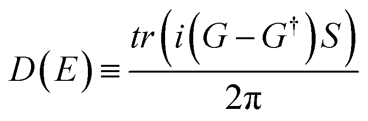
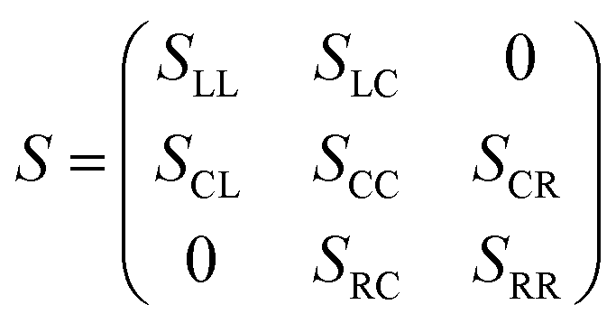
where SLL and SRR denote the contribution of the left and right electrodes, respectively, SLC (SRC) expresses the interaction between the scattering area and the left (right) electrode, and SCC denotes the contribution of the scattering area.
3. Results and discussion
Considering the anisotropy of the electron transport properties in some 2D materials, such as black phosphorene39 and ReS2,40 we have first compared the electron transport properties of the 2D PtSe2 nanosheet with electron transport along two different directions. The insets in Fig. 1(a) and (c) illustrate the top and side views of the PtSe2 nanosheets with different chirality, respectively. For simplicity, we apply the nomenclature of a(z)-PtSe2-nanosheet to define the nanosheet, where a- and z-represent the armchair and zigzag chirality, respectively, i.e., the chirality of the nanosheet in the direction of electron transport. It can be seen from their I–V curves that no matter which direction the electrons flow along, it is difficult for the nanosheets to conduct, and their currents are thus maintained at 0 before the voltage reaches 1.5 V. When the voltage continues to increase, the nanosheet device turns on. However, electron conduction along the armchair direction is more favorable than that along the zigzag direction, and the conductivity of the former is five times higher than that of the latter. In order to evaluate the intrinsic physical mechanism of the electron transport difference between these two directions, we calculated the electronic band structures of the a-PtSe2-nanosheet and z-PtSe2-nanosheet unit cells, as shown in Fig. 1(b) and (d), respectively.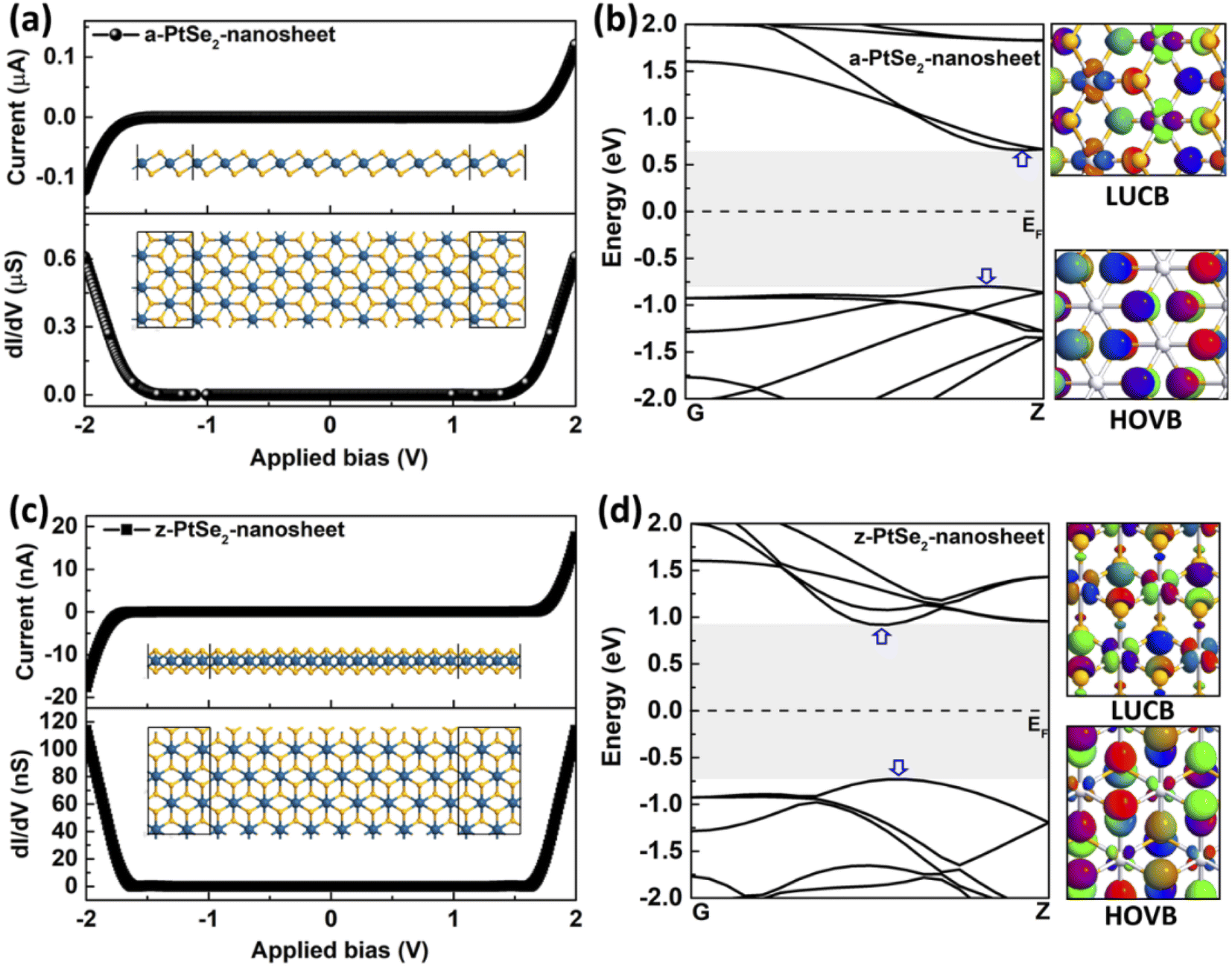 | ||
| Fig. 1 Electronic properties of PtSe2 nanosheets with different chirality. (a) Current–voltage curve and conductance spectrum of the a-PtSe2 nanosheet device as well as the top and side views of the atomic structures. (b) Band structures of the a-PtSe2-nanosheet with unit cells of 2Pt and 4Se atoms as well as the Bloch states at the points marked with a blue arrow of HOVB and LUCB with an isovalue of 0.15. (c) Current–voltage curve and conductance spectrum of the z-PtSe2 nanosheet device as well as the top and side views of the atomic structures. (d) Band structures of the z-PtSe2-nanosheet with unit cells of 2Pt and 4 Se atoms as well as the Bloch states at the points marked with a blue arrow of HOVB and LUCB with an isovalue of 0.15. The Fermi level is set to zero. G (0, 0, 0) and Z (0, 0, 0.5) refer to the high-symmetric k-points in the first Brillouin zone. | ||
Both the a-PtSe2-nanosheet and z-PtSe2-nanosheet have indirect band gap semiconducting characteristics, but they have different energy gaps of 1.46 eV and 1.65 eV, respectively, which is close to the results of a previous work.41,42 Because the band gap of the a-PtSe2-nanosheet is significantly lower than that of the z-PtSe2-nanosheet, the electrons in the a-PtSe2-nanosheet are more easily excited from the valence band and transferred to the conduction band, which results in higher conductivity. Moreover, their Bloch states at the points marked with blue arrows of the HOVB and LUCB are calculated, which reflects the distribution of electrons in the nanosheets. The electrons in the HOVB of the a-PtSe2-nanosheet mainly distribute at Se atoms, indicating that it is the p orbitals of the Se atoms that are responsible for the band structure. For the LUCB of the a-PtSe2-nanosheet, however, the electrons are mainly from the d orbital of Pt atoms and the p orbitals of Se atoms. Unlike the a-PtSe2-nanosheet, the electrons in the HOVB and LUCB of the z-PtSe2-nanosheet distribute at both Se and Pt atoms. This electronic structure difference leads to the different electron transport properties of the PtSe2 nanosheets along the two directions.
It is well known that edge reconstruction is common in two-dimensional materials such as graphene,3,4,43 MoS2 (ref. 13 and 44) and BN5 during CVD growth, and it plays a critical role in controlling the electronic, magnetic, and optical properties. Next, we propose a series of PtSe2 nanoribbons with different chiralities and edges; their atomic structures, as shown in Fig. 2(a), are represented as a-PtSe2-edge1, a-PtSe2-edge2, z-PtSe2-edge1, z-PtSe2-edge2 and z-PtSe2-edge3. To evaluate the structural stability and analysis, we also calculated the formation energies of the edges. The results are given in Table 1. In addition, to better represent the composition of the edge, the ratios of Pt to Se atoms at the edge are given as follows:  , where NPt and NSe are the number of Pt and Se atoms at the edges, respectively.
 | ||
| Fig. 2 (a) Schematic of the PtSe2 nanoribbon two-probe nanodevice and the atomic structures of a-PtSe2-edge1, a-PtSe2-edge2, z-PtSe2-edge1, z-PtSe2-edge2 and z-PtSe2-edge3. The blue and yellow balls represent Pt and Se atoms, respectively. (b) Equilibrium transmission spectrum, (c) density of states, (d) current–voltage curve and conductance spectra, and (e) transmission spectra for different biases of the a-PtSe2-edge1 device. The color bar shows the electron transmission probability. | ||
| Edge | a-PtSe2-edge1 | a-PtSe2-edge2 | z-PtSe2-edge1 | z-PtSe2-edge2 | z-PtSe2-edge3 |
|---|---|---|---|---|---|
| R | 1:4 |
1:2 |
1:2 |
1:2 |
1:1 |
| Ef (eV nm−1) | 6.90 | 6.55 | 6.18 | 7.06 | 6.66 |
The formation energy of each nanoribbon is calculated using the following formula:

Fig. 2(b) shows the equilibrium transmission spectrum of the a-PtSe2-edge1 two-probe device, which has a Se-rich edge and the ratio of Pt to Se atoms at the edge is 1:4. It is worth noting that the transmission possibility at the Fermi level with zero applied bias is higher than 1, demonstrating that there are more than one electronic transport channels at the Fermi level, i.e., it will have a high current value at low bias. The projected density of states shows the contribution of the Pt-d and Se-p orbitals to the total density of states, from which we can conclude that the total density of states near the Fermi level mainly comes from the Se-p orbitals at the edges. That is to say, the edges play an important role in the conduction of electrons in these nanoribbon devices. We have also calculated the non-equilibrium electron transport property of a-PtSe2-edge1 device, as shown in Fig. 2(d). As predicted from the equilibrium transmission spectrum, the current increases sharply when a small bias is applied and reaches a maximum of 30.05 μA when the applied bias increases to 0.35 V. Then, the current decreases when the bias continues to increase, leading to an obvious NDR effect. Notably, for the a-PtSe2-edge1 two-probe device, the current increases faster when the applied bias ranges from 0 to 0.2 V, resulting in high conductance (about 100 μS). Then, the conductance decreases when the applied bias is greater than 0.2 V, which corresponds to the slow increase in current in the range of 0.2 to 0.35 V. Finally, the conductance becomes negative, which occurs due to the NDR effect.
For a deep insight into the NDR effect, its transmission spectra under different biases are given in Fig. 2(e), which reflect the electron transmission probability within the bias window. The two dashed lines indicate the bias windows. As the applied bias increases from 0 to 1.0 V, the chemical potential of the source (drain) electrode μ1 (μ2) decreases (increases) by 0.5 eV. Furthermore, the electron transmission probability within the bias window becomes increasingly obvious as the applied bias increases from zero to 0.35 V, which implies that the transmission via the tunneling effect around the Fermi level increases. Such changes in the transmission spectra in the μ1–μ2 bias window cause an exponential increase in current from 0 to 0.35 V. When the applied bias is higher than 0.35 V, the electron transmission probability within the bias window becomes lower, which leads to decreasing current. This electron transmission probability tendency within the bias window is the intrinsic cause of the NDR in the I–V curve.
Unlike the a-PtSe2-edge1 device, the electron transmission ability of the a-PtSe2-edge2, which has a ratio of Pt to Se atoms at the edge of 1:2, is much lower than that of the former, as shown in Fig. 3(a). Its current increases exponentially over the applied bias range of 0–0.25 V, remains steady at about 10 μA from 0.25 to 0.4 V, and then increases gradually to 16.66 μA at 0.65 V. Finally, its current decreases with the applied bias, resulting in the NDR phenomenon. The conductance at 0 V is 65.32 μS and then decreases with a bias from 0 to 0.25 V. Thereafter, it is maintained at about zero at a bias range of 0.25 to 0.4 V. As the applied bias continues to increase, the conductance first increases and then decreases gradually, similar to the current tendency. Finally, the conductance becomes negative, which is also due to the NDR effect of a-PtSe2-edge2. Fig. 3(b) shows its transmission spectra under different biases. Obviously, its electron transmission probability is much lower than that of a-PtSe2-edge1, and thus, its current is lower than that of a-PtSe2-edge1.
 | ||
| Fig. 3 Electron transport properties of the a-PtSe2-edge2 and z-PtSe2-edge1 devices. (a) Current–voltage curve, conductance spectra and (b) transmission spectra under different biases of the a-PtSe2-edge2 device. (c) Current–voltage curve, conductance spectra and (d) transmission spectra under different biases of the z-PtSe2-edge1 device. | ||
For the z-PtSe2 nanoribbon, we propose three different edges of the ‘Pt–Se–Pt–Se’, ‘Se–Pt–Se–Se–Pt’, and ‘Se–Pt–Se–Pt’ forms, denoted by z-PtSe2-edge1, z-PtSe2-edge2 and z-PtSe2-edge3, respectively. Fig. 3(c and d) illustrate the electron transport properties of the z-PtSe2-edge1 device, which exhibits semiconducting characteristics. Specifically, the current of z-PtSe2-edge1 is zero when the applied bias is below 0.17 V since there is no electron transmission peak within the bias window. With the increase in the applied bias, the bias window continues to expand, and small electron transmission peaks appear. Thus, the current gradually increases with increasing bias and reaches a maximum of 25.74 μA at 0.6 V. Although the bias window continues to expand when the bias exceeds 0.6 V, the transmission probability in the bias window decreases. Therefore, the current of z-PtSe2-edge1 gradually decreases, resulting in the NDR effect in the I–V curve, as shown in Fig. 3(c).
It is worth noting that the ratios of Pt to Se atoms at the edge for both a-PtSe2-edge2 and z-PtSe2-edge1 are 1:2, but the former is metallic while the latter is semiconducting. What about the other zigzag PtSe2 nanoribbon device with a Pt to Se ratio of 1:2 at the edge (z-PtSe2-edge2)? Fig. 4(a and b) demonstrate the electron transport properties of the z-PtSe2-edge2 nanoribbon device. Similar to z-PtSe2-edge1, z-PtSe2-edge2 also shows a semiconducting property. Its current is zero before the applied bias reaches 0.3 V, which is attributed to the negligible electron transmission peak within the bias window. With increasing applied bias, the current increases gradually, but its maximum current is only 4.45 μA at 0.6 V, much lower than that of z-PtSe2-edge1. Their similar I–V curves contribute to a similar trend in their conductance spectra.
 | ||
| Fig. 4 Electron transport properties of the z-PtSe2-edge2 and z-PtSe2-edge3 devices. (a) Current–voltage curve, conductance spectra and (b) transmission spectra under different biases of the z-PtSe2-edge2 device. (c) Current–voltage curve, conductance spectra and (d) transmission spectra under different biases of the z-PtSe2-edge3 device. | ||
z-PtSe2-edge3 is totally different from the former two in terms of its electron transport properties, where the edge is reconstructed to be the ‘Se–Pt–Se–Pt’ form, although all of them are of the zigzag type. It has a Se-poor edge, and the ratio of Pt to Se atoms at the edge is 1:1. Unexpectedly, it has similar electron transport properties as a-PtSe2-edge2. The z-PtSe2-edge3 device is metallic, and its current increases sharply with increasing bias and then decreases gradually. This phenomenon reflects that the influence of edge reconstruction on the electron transport properties of PtSe2 nanoribbons is more significant than that of chirality.
We next analyze the transmission spectra and the primary transmission eigenstates of a-PtSe2-edge2 and z-PtSe2-edge3 to compare their differences, as shown in Fig. 5. The electronic transmission eigenstate is a wave function of the electron, which represents the scattering state of the electron from the source electrode to the drain electrode. Although their current values at 0.65 V are very close, their current sources are different. From the electron transmission spectrum of the a-PtSe2-edge2 device, it can be seen that there is an obvious electron transmission peak at the Fermi level at 0.65 V, where there is only one electron projection channel with a transmission eigenvalue of 0.224, and the electrons are mainly conducted through the Pt and Se atoms at the edges with π characteristics. The electron transmission probability of the z-PtSe2-edge3 device at the Fermi level is 0, and its current value is contributed by the electron transmission peak at 0.24 eV in the bias window. The electrons propagate along the Pt atoms at the edges, and the Pt-d orbitals make a difference. That is to say, although the I–V curves of a-PtSe2-edge2 and z-PtSe2-edge3 are very similar, the channels that play a major role in electron transport are still different.
 | ||
| Fig. 5 (a) Transmission spectra under 0.65 V and the primary transmission eigenstate at the Fermi level with an isovalue of 0.07 for the a-PtSe2-edge2 device. (b) Transmission spectra under 0.65 V and the primary transmission eigenstate at −0.24 eV with an isovalue of 0.4 of the z-PtSe2-edge3 device. The vertical dashed lines indicate the chemical potential of the left electrode μ1 (left) and the right electrode μ2 (right). | ||
As indicated by the I–V curves of the PtSe2 nanoribbons, these devices show different NDR effects. The peak-to-valley current ratio (PVCR) voltage-controlled NDR character represents the extent of the NDR effect, which is defined as  . The calculated PVCRs of these devices are shown in Table 2. For example, a-PtSe2-edge2 has the highest PVCR, demonstrating that its NDR effect is the strongest.
| Edge | a-PtSe2-edge1 | a-PtSe2-edge2 | z-PtSe2-edge1 | z-PtSe2-edge2 | z-PtSe2-edge3 |
|---|---|---|---|---|---|
| Ipeak (μA) | 30.05 | 16.66 | 25.74 | 4.45 | 13.59 |
| Ivalley (μA) | 7.69 | 3.22 | 12.16 | 1.51 | 9.36 |
| PVCR | 3.91 | 5.17 | 2.12 | 2.95 | 1.45 |
We have calculated their electronic structures to elucidate their different electron transport properties. Given that the electron distributions near the Fermi level determine the electron transport properties of these nanoribbon devices, we also provide the Bloch states of the bands near the Fermi level (Fig. 6). For a-PtSe2-edge1, one band crosses the Fermi level, endowing the a-PtSe2-edge1 device with metallic conducting characteristics and high conductivity. The electrons in this band mainly distribute on the Se atoms of the edge, which dominates the conduction of electrons. This phenomenon is consistent with the aforementioned DOS results of the a-PtSe2-edge1 device. For a-PtSe2-edge2 and z-PtSe2-edge3, which both show metallic electronic properties, their electrons are also located at the edges.
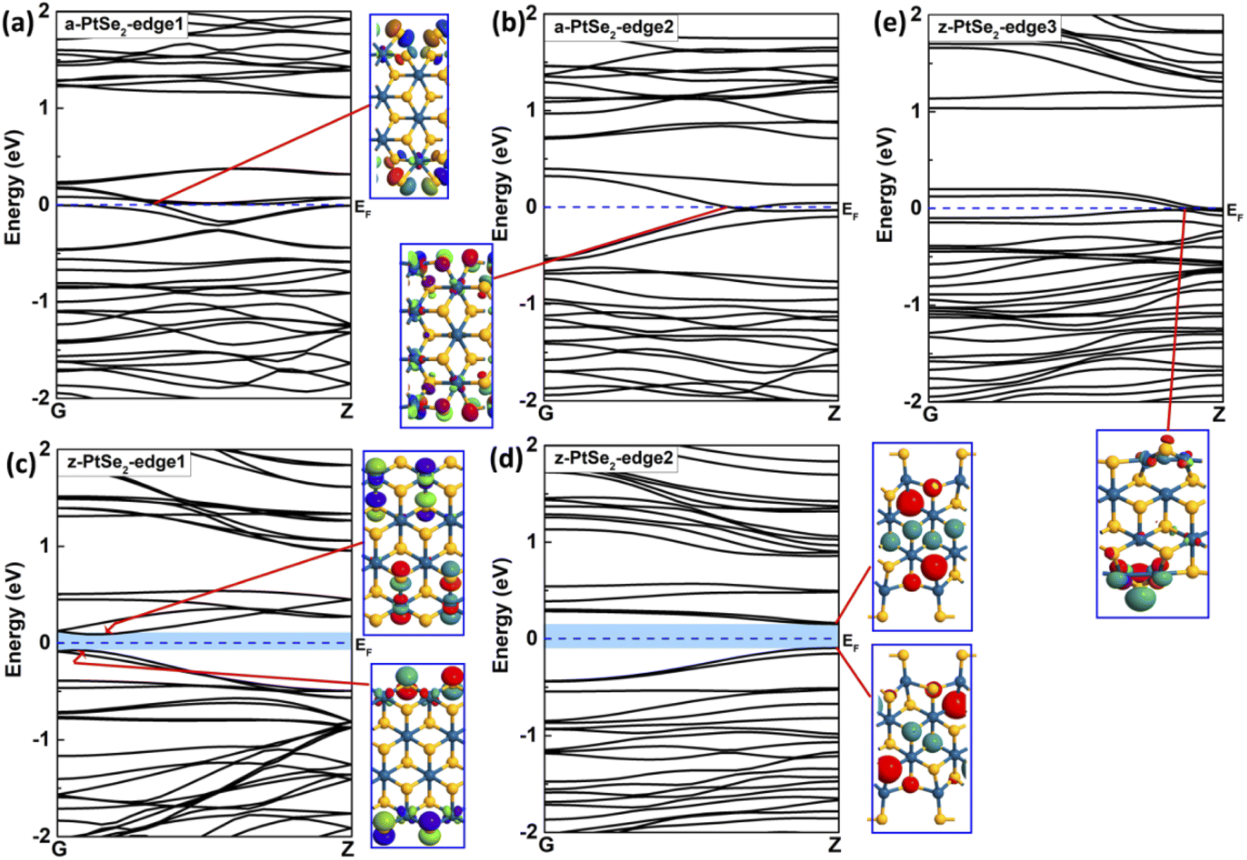 | ||
| Fig. 6 Band structures of (a) the a-PtSe2-edge1 and (b) the a-PtSe2-edge2 unit cells as well as the Bloch states at the points marked with a red line of the band crossing the Fermi level with an isovalue of 0.1. Band structures of (c) the z-PtSe2-edge1 and (d) the z-PtSe2-edge2 unit cells as well as the Bloch states at the points marked with red line of the HOVB (bottom) and LUCB (top) with an isovalue of 0.1. (e) Band structures of the z-PtSe2-edge3 unit cell and the Bloch states at the points marked with a red line of the band crossing the Fermi level with an isovalue of 0.1. The Fermi level is set to zero. G (0, 0, 0) and Z (0, 0, 0.5) refer to the high-symmetric k-points in the first Brillouin zone. | ||
For z-PtSe2-edge1 and z-PtSe2-edge2, band gaps emerge at their band structures with energy gaps of 0.17 and 0.25 eV, respectively, which explains the existence of a platform with a current of zero in their I–V curves under low bias. However, their electron distributions are completely different. In z-PtSe2-edge1, electrons of the HOVB concentrate on the Se atoms of the edges, while those of the LUCB concentrate on the Pt atoms of the edges, and the Se atoms are connected vertically with these Pt atoms. For z-PtSe2-edge2, electrons of the HOVB and LUCB are both located at the Se atoms in the central region. Their different electronic structures lead to the variety of electron transport properties that change with the edge reconstructions.
4. Conclusion
In summary, based on the DFT and NEGF methods, we show that the various edge reconstructions of the PtSe2 nanoribbon can not only significantly affect the electron transport properties of the devices but also enable distinctive NDR behaviors in the PtSe2 nanoribbon devices. DFT calculations demonstrate that the armchair PtSe2 nanoribbons with ratios of Pt to Se atoms at the edge of 1:4 and 1:2 are both metallic, while the zigzag PtSe2 nanoribbons are semiconducting when the ratio of Pt to Se atoms at the edge is 1:2, reflecting the significant effect of edge reconstruction on the electronic properties of PtSe2 nanoribbons. Moreover, even for the same zigzag nanoribbons, when the ratio of Pt to Se atoms at the edge is 1:1, their electronic properties are no longer similar to those of the zigzag nanoribbons with a Pt to Se ratio of 1:2 at the edge, but similar to that of the armchair nanoribbon with the same Pt to Se ratio of atoms at the edge. This phenomenon reflects that the influence of edge reconstruction on the electron transport properties of PtSe2 nanoribbons is even more significant than that of chirality. Our findings provide fundamental insights into the role of edge reconstruction on the electronic properties of PtSe2 nanoribbons and provide new ideas for the design of PtSe2 semiconducting and conducting electronic nanodevices with NDR behavior by introducing different edge reconstructions, which has great potential applications in electronic devices.
Author contributions
All authors have given their approval to the final version of the manuscript.Conflicts of interest
The authors declare no competing financial interest.Acknowledgements
The authors would like to acknowledge the support from the National Natural Science Foundation of China (U1806219 and 52171038) and Shanghai Sailing Program (Grant No. 22YF1413000). Special funding also supports this work via the Project of the Qilu Young Scholar Program of Shandong University and the Project of the Taishan Scholar Construction Engineering.References
- K. S. Novoselov, A. K. Geim, S. V. Morozov, D. Jiang, M. I. Katsnelson, I. V. Grigorieva, S. V. Dubonos and A. A. Firsov, Nature, 2005, 438, 197–200 CrossRef CAS PubMed.
- Y.-W. Son, M. L. Cohen and S. G. Louie, Phys. Rev. Lett., 2006, 97, 216803 CrossRef PubMed.
- K. He, A. W. Robertson, Y. Fan, C. S. Allen, Y.-C. Lin, K. Suenaga, A. I. Kirkland and J. H. Warner, ACS Nano, 2015, 9, 4786–4795 CrossRef CAS PubMed.
- K. Kim, S. Coh, C. Kisielowski, M. Crommie, S. G. Louie, M. L. Cohen and A. Zettl, Nat. Commun., 2013, 4, 1–6 Search PubMed.
- J. Deng, Y. Yin, H. Niu, X. Ding, J. Sun and N. V. Medhekar, Sci. Rep., 2017, 7, 7855 CrossRef PubMed.
- M. Wu, X. Wu, Y. Pei and X. C. Zeng, Nano Res., 2011, 4, 233–239 CrossRef CAS.
- L. Liang, J. Wang, W. Lin, B. G. Sumpter, V. Meunier and M. Pan, Nano Lett., 2014, 14, 6400–6406 CrossRef CAS PubMed.
- P. Cui, J.-H. Choi, W. Chen, J. Zeng, C.-K. Shih, Z. Li and Z. Zhang, Nano Lett., 2017, 17, 1097–1101 CrossRef CAS PubMed.
- M. C. Lucking, J. Bang, H. Terrones, Y.-Y. Sun and S. Zhang, Chem. Mater., 2015, 27, 3326–3331 CrossRef CAS.
- Y. Chen, P. Cui, X. Ren, C. Zhang, C. Jin, Z. Zhang and C.-K. Shih, Nat. Commun., 2017, 8, 1–9 CrossRef PubMed.
- F. Yao, Z. Xiao, J. Qiao, W. Ji, R.-J. Xie and C. Jin, Nanoscale, 2021, 13, 4133–4139 RSC.
- A. Ghosh, M. Kar, C. Majumder and P. Sarkar, Phys. Chem. Chem. Phys., 2021, 23, 1127–1138 RSC.
- W. Zhou, X. Zou, S. Najmaei, Z. Liu, Y. Shi, J. Kong, J. Lou, P. M. Ajayan, B. I. Yakobson and J.-C. Idrobo, Nano Lett., 2013, 13, 2615–2622 CrossRef CAS PubMed.
- Y. Li, Z. Zhou, S. Zhang and Z. Chen, J. Am. Chem. Soc., 2008, 130, 16739–16744 CrossRef CAS PubMed.
- A. R. Botello-Méndez, F. Lopez-Urias, M. Terrones and H. Terrones, Nanotechnology, 2009, 20, 325703 CrossRef.
- K. Chen, J. Deng, X. Ding, J. Sun, S. Yang and J. Z. Liu, J. Am. Chem. Soc., 2018, 140, 16206–16212 CrossRef CAS PubMed.
- X. Deng, Z. Li and J. Yang, J. Phys. Chem. Lett., 2020, 11, 7531–7535 CrossRef CAS PubMed.
- Y. Liu, D. Li and T. Cui, Nanoscale, 2021, 13, 4085–4091 RSC.
- L. P. Ding and F. Ding, Nanoscale Horiz., 2021, 6, 148–155 RSC.
- Y. Wang, L. Li, W. Yao, S. Song, J. T. Sun, J. Pan, X. Ren, C. Li, E. Okunishi, Y.-Q. Wang, E. Wang, Y. Shao, Y. Y. Zhang, H.-t. Yang, E. F. Schwier, H. Iwasawa, K. Shimada, M. Taniguchi, Z. Cheng, S. Zhou, S. Du, S. J. Pennycook, S. T. Pantelides and H.-J. Gao, Nano Lett., 2015, 15, 4013–4018 CrossRef CAS PubMed.
- Y. Zhao, J. Qiao, Z. Yu, P. Yu, K. Xu, S. P. Lau, W. Zhou, Z. Liu, X. Wang, W. Ji and Y. Chai, Adv. Mater., 2017, 29, 1604230 CrossRef PubMed.
- C. Yim, K. Lee, N. McEvoy, M. O'Brien, S. Riazimehr, N. C. Berner, C. P. Cullen, J. Kotakoski, J. C. Meyer and M. C. Lemme, ACS Nano, 2016, 10, 9550–9558 CrossRef CAS PubMed.
- Z. Wang, Q. Li, F. Besenbacher and M. Dong, Adv. Mater., 2016, 28, 10224–10229 CrossRef CAS PubMed.
- H. Xu, H. Zhang, Y. Liu, S. Zhang, Y. Sun, Z. Guo, Y. Sheng, X. Wang, C. Luo and X. Wu, Adv. Funct. Mater., 2019, 29, 1805614 CrossRef.
- L. H. Zeng, D. Wu, S. H. Lin, C. Xie, H. Y. Yuan, W. Lu, S. P. Lau, Y. Chai, L. B. Luo and Z. J. Li, Adv. Funct. Mater., 2019, 29, 1806878 CrossRef.
- L. H. Zeng, S. H. Lin, Z. J. Li, Z. X. Zhang, T. F. Zhang, C. Xie, C. H. Mak, Y. Chai, S. P. Lau and L. B. Luo, Adv. Funct. Mater., 2018, 28, 1705970 CrossRef.
- L. H. Zeng, Q. M. Chen, Z. X. Zhang, D. Wu, H. Yuan, Y. Y. Li, W. Qarony, S. P. Lau, L. B. Luo and Y. H. Tsang, Adv. Sci., 2019, 6, 1901134 CrossRef CAS PubMed.
- D. Wu, J. Guo, J. Du, C. Xia, L. Zeng, Y. Tian, Z. Shi, Y. Tian, X. J. Li and Y. H. Tsang, ACS Nano, 2019, 13, 9907–9917 CrossRef CAS PubMed.
- L. Zeng, D. Wu, J. Jie, X. Ren, X. Hu, S. P. Lau, Y. Chai and Y. H. Tsang, Adv. Mater., 2020, 32, 2004412 CrossRef PubMed.
- D. Wu, J. Guo, C. Wang, X. Ren, Y. Chen, P. Lin, L. Zeng, Z. Shi, X. J. Li and C.-X. Shan, ACS Nano, 2021, 15, 10119–10129 CrossRef PubMed.
- D. Wu, Z. Zhao, W. Lu, L. Rogée, L. Zeng, P. Lin, Z. Shi, Y. Tian, X. Li and Y. H. Tsang, Nano Res., 2021, 14, 1973–1979 CrossRef CAS.
- D. Wu, M. Xu, L. Zeng, Z. Shi, Y. Tian, X. J. Li, C.-X. Shan and J. Jie, ACS Nano, 2022, 16, 5545–5555 CrossRef CAS PubMed.
- M. Brandbyge, J.-L. Mozos, P. Ordejón, J. Taylor and K. Stokbro, Phys. Rev. B: Condens. Matter Mater. Phys., 2002, 65, 165401 CrossRef.
- E. Engel and R. M. Dreizler, Density Functional Theory, Springer, 2013 Search PubMed.
- J. P. Perdew, K. Burke and M. Ernzerhof, Phys. Rev. Lett., 1996, 77(18), 3865 CrossRef CAS PubMed.
- QuantumATK version 2017.2, Synopsys QuantumATK, https://www.synopsys.com/silicon/quantumatk.html Search PubMed.
- D. Stradi, U. Martinez, A. Blom, M. Brandbyge and K. Stokbro, Phys. Rev. B, 2016, 93, 155302 CrossRef.
- J. Q. You, C.-H. Lam and H. Z. Zheng, Phys. Rev. B: Condens. Matter Mater. Phys., 2000, 62, 1978–1983 CrossRef CAS.
- H. D. Bui and M. Yarmohammadi, Solid State Commun., 2018, 280, 39–44 CrossRef CAS.
- R. Wang, F. Zhou, L. Lv, S. Zhou, Y. Yu, F. Zhuge, H. Li, L. Gan and T. Zhai, CCS Chem., 2019, 1, 268–277 CAS.
- G. Wang, K. Wang, N. McEvoy, Z. Bai, C. P. Cullen, C. N. Murphy, J. B. McManus, J. J. Magan, C. M. Smith and G. S. Duesberg, Small, 2019, 15, 1902728 CrossRef.
- Z. Guan, S. Ni and S. Hu, RSC Adv., 2017, 7, 45393–45399 RSC.
- L. Song, X. Zheng, R. Wang and Z. Zeng, J. Phys. Chem. C, 2010, 114, 12145–12150 CrossRef CAS.
- X. Sang, X. Li, W. Zhao, J. Dong, C. M. Rouleau, D. B. Geohegan, F. Ding, K. Xiao and R. R. Unocic, Nat. Commun., 2018, 9, 1–7 CrossRef.
| This journal is © The Royal Society of Chemistry 2022 |