
 Open Access Article
 This Open Access Article is licensed under a Creative Commons Attribution-Non Commercial 3.0 Unported Licence
Eu- and Tb-adsorbed Si3N4 and Ge3N4: tuning the colours with one luminescent host†
Cordula Braun *a,
Liuda Mereacrea,
Zheng Chenb,
Adam Slabonc,
David Vincentd,
Xavier Rocquefelted and
Jean-François Halete
*a,
Liuda Mereacrea,
Zheng Chenb,
Adam Slabonc,
David Vincentd,
Xavier Rocquefelted and
Jean-François Halete
aKarlsruhe Institute of Technology (KIT), Institute for Applied Materials (IAM), Herrmann-von-Helmholtz-Platz 1, D-76344 Eggenstein-Leopoldshafen, Germany. E-mail: Cordula.Braun@kit.edu
bInstitute of Inorganic Chemistry, RWTH Aachen University, Landoltweg 1, D-52056 Aachen, Germany
cChair of Inorganic Chemistry, University of Wuppertal, Gaussstr. 20, 42119 Wuppertal, Germany
dUniv. Rennes – CNRS, Institut des Sciences Chimiques de Rennes, UMR 6226, 35042 Rennes, France
eCNRS – Saint-Gobain – NIMS, IRL 3629, Laboratory for Innovative Key Materials and Structures (LINK), National Institute for Materials Science (NIMS), 1-1 Namiki, Tsukuba 305-0044, Japan
First published on 10th November 2022
Abstract
Phosphor-converted white light emitting diodes (pc-LEDs) are efficient light sources for applications in lighting and electronic devices. Nitrides, with their wide-ranging applicability due to their intriguing structural diversity, and their auspicious chemical and physical properties, represent an essential component in industrial and materials applications. Here, we present the successful adsorption of Eu and Tb at the grain boundaries of bulk β-Si3N4 and β-Ge3N4 by a successful combustion synthesis. The adsorption of europium and terbium, and the synergic combination of both, resulted in intriguing luminescence properties of all compounds (red, green, orange and yellow). In particular, the fact that one host can deliver different colours renders Eu,Tb-β-M3N4 (M = Si, Ge) a prospective chief component for future light emitting diodes (LEDs). For the elucidation of the electronic properties and structure of β-Si3N4 and β-Ge3N4, Mott–Schottky (MS) measurements and density functional theory (DFT) computations were conducted for the bare and RE adsorbed samples.
Main
Phosphor-converted white light-emitting diodes (pc-LEDs) are emerging as an indispensable solid-state light source for the next generation lighting industry and display systems due to their unique properties.1,2Doped gallium nitride (GaN) has been the benchmark in the past decades in this domain and has indeed driven the LED revolution in lighting and displays as a key material. The concept of down-conversion of a GaN-based blue LED, being awarded the Nobel prize in 2014 in physics,3–5 offers the possibility to provide efficient generation of monochromatic, high-colour purity light resulting in a highly efficient warm-white all-nitride phosphor-converted light emitting diode (pc-LED). The combination of the lower energy consumption, high light quality, preservation of colour point stability and long lifetime is one of the key benefits of pc-LEDs, having the potential to reduce global energy consumption in the lighting sector substantially.
Silicon nitride (Si3N4) high performance ceramics are used in numerous applications because of their superior mechanical properties.6,7 The wide-ranging applicability of nitrides and their related (oxo)nitridosilicate family can be ascribed to their significantly extended structural varieties as well as their auspicious chemical and physical properties (very high chemical and thermal stability, very high quantum efficiency, very low thermal quenching).
In particular, Eu2+-doped (oxo)nitridosilicates and SiAlONs have been amply studied as important host lattices for phosphor-converted light-emitting diodes (pc-LEDs).8–25
For instance, M2Si5N8:Eu2+ (red-orange, 2-5-8 phosphor) and MSi2O2N2:Eu2+ (yellow-green, 1-2-2-2 phosphor) (M = Ca, Sr, Ba) were significant discoveries in this field. Several Mg-nitridosilicates and nitridoaluminates were also developed as next generation high efficient red emitting phosphor materials with superior luminescence properties.26–30
The next step in phosphor development is the investigation of novel host materials for narrow-band emitting phosphors to enhance luminous efficacy and improving therefore the quality of light emitting diodes (LEDs) for diverse applications upon doping.
Silicon nitride (Si3N4) materials have been found to meet these requirements due to its rigid lattices with highly covalent network and high thermal stability.31,32 However, looking at the literature indicates that there are only a few investigations concerning rare-earth doped silicon nitride materials. In most cases only Eu- and Tb-doped α-Si3N4 thin films and nanowires illustrating broad band emission are concerned.33–41 Here we use the expression doping explicitly as this is given in the references.
There are many works in the literature regarding the influence of rare-earth oxides additives often defining the morphology of β-Si3N4 crystallites growing in a multiphase ceramic, thereby affecting its microstructure and mechanical toughness of the ceramic.42–49 Densification additives (e.g., rare-earth (RE) oxides) play an important role in the fabrication of silicon nitride-based ceramics. Indeed, the affinity of the RE cations to segregate and adsorb on the prismatic planes of the hexagonal grains in β-Si3N4, exhibiting very anisotropic shapes, is used to develop microstructural features (e.g., the initiation of the α,β-transformation and the formation of elongated reinforcing grains) required for particular applications.43
Phosphors are usually doped with Eu2+ and only one activator ion is used. Therefore, one host shows one colour. The fact that nitride bulk material can be doped with several rare-earth activator ions, even at the same time, is absolutely new resulting in the fact that one host can deliver different colours.
As well novel is the fact that a pure nitride host material shows green luminescence,31,32 till now this could only be realized by oxynitrides and oxonitridosilicates.18,50–53
Just recently we demonstrated that the so called “yellow gap” could be closed for bulk GaN via co-doping with europium and terbium.32 Co-doping really opens up a multitude of degrees of freedom to customize and adapt a luminescent material to specific needs.
Herein, we experimentally and theoretically examine the adsorption of Eu and Tb at the grain boundaries of β-Si3N4 and β-Ge3N4 and discuss their resulting intriguing luminescence properties.
At this point we would like to point out that we explicitly talk here of adsorption of the RE elements and not of doping. In the nitridosilicate Ca2Si5N8:Eu2+ the RE cations go the Ca site of the host structure, which is named doping. But there is no analogous cation site in β-Si3N4 and β-Ge3N4.
As described in detail in literature43,44,49 the RE cations go to the grain boundaries in β-Si3N4. Therefore we choose the term Eu adsorbed-Si3N4 and not doped as it is used for e.g. Eu-doped nitridosilicates. For a detailed discussion concerning this topic we would like to refer to lit.43,44,49 and the section below, where a detailed explanation of the RE adsorption sites is given.
(For β-Si3N4 and β-Ge3N4 adsorbed with europium and/or terbium we would like to introduce the notation Eu,Tb-β-M3N4.) The results indicate that Eu,Tb-β-Si3N4 (ref. 31) and as well as Eu,Tb-β-Ge3N4 (ref. 31) should be considered as prospective chief components for highly efficient warm-white all-nitride phosphor-converted light emitting diode (pc-LED).
Results
Structure and composition characterization
A low temperature urea-based synthetic approach was successfully used to combine β-Si3N4 and β-Ge3N4 (Chempur 99![[thin space (1/6-em)]](https://www.rsc.org/images/entities/char_2009.gif) 999%) with MCl3·x6H2O or M(NO3)3·x5H2O (M = Eu, Tb). (see Fig. 1a and S1–S3†).31
999%) with MCl3·x6H2O or M(NO3)3·x5H2O (M = Eu, Tb). (see Fig. 1a and S1–S3†).31
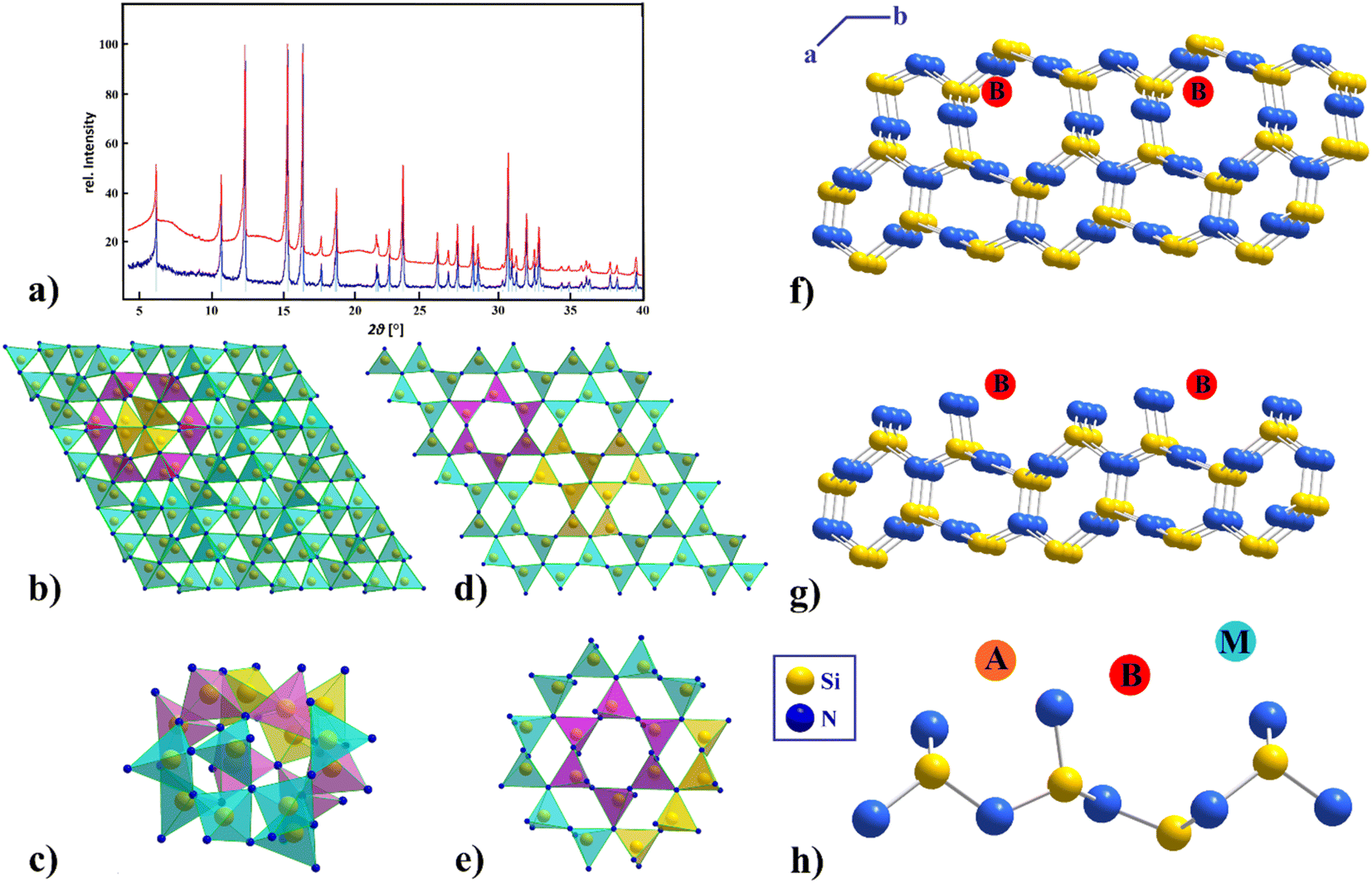 | ||
| Fig. 1 (a) X-ray powder diffraction patterns of pure β-Si3N4 (blue), adsorbed Eu-β-Si3N4 (red) and the bar graph of β-Si3N4 ICSD [33-1160] (bright blue), (λ = 0.709026 Å), (b) structure of α-Si3N4 view along [001], (c) cavity for a possible insertion of a RE cation in α-Si3N4, (d) structure of β-Si3N4 view along [001], (e) six-ring representation of β-Si3N4, (f, g and h) structure of β-Si3N4 view along [001] with three possible RE adsorption sites A, B, and M.44 (Si atoms are depicted in yellow, N atoms in blue, the RE adsorption sites A, B, and M in orange, red and light blue). | ||
For a comparison of the powder diffraction patterns of Eu-β-Si3N4 and Tb-β-Si3N4 see Fig. S1,† for Tb-β-Ge3N4 and Eu,Tb-β-Ge3N4, see Fig. S3.† SEM EDX measurements of β-Si3N4 and β-Ge3N4 confirmed the atomic ratio of M:N (M = Si, Ge) of 3:4 and europium and terbium contents of 3–5% were found (see Fig. S4†).
Understanding the influence of selective dopant additions and the role of interfacial interactions is central to the design of novel high-performance Si3N4 ceramics by offering the potential for customizing the materials properties. Rare-earth cations are often located within regions of the oxynitride glassy phase of triple-junction pockets, disordered amorphous nanometer scale intergranular films (IGF) and at the glass or IGF/β-Si3N4 grain interfaces.44
According to the literature44,49 there are three independent stable RE adsorption sites per surface unit cell along the N-terminated prismatic planes of β-Si3N4 (see Fig. 1f–h). A and B are stable RE equilibrium sites, while calculations pretended the M site to be theoretically unstable, although observed experimentally in the case of La adsorption.44 Stereochemical bonding factors are found to determine the adsorption site preferences contrary to ionic size effects, and the strength of the rare-earth interface bonding is defined inter alia by the electronic structure of the nitride surface. Shibata et al.49 showed that these RE adsorption sites have higher binding energies than Si, partially reside on cation sites normally only available for Si and that the RE–N bonds are longer than comparable Si–N bonds. While in β-Si3N4 an adsorption of the RE ions at the grain boundaries is possible (see Fig. 1f–h), in α-Si3N4 an insertion of cations into the structure (see Fig. 1c) takes place. In the α-Si3N4 structure there are two caves (for the bigger one see Fig. 1c), which can be occupied when charge is balanced by cation and/or anion substitutions (e.g., Si by Al and N by O). This additional insertion of an RE ion is stabilizing the α-Si3N4, which is otherwise metastable.54 And indeed, no insertion of cations is realized into the six rings in β-Si3N4 (see Fig. 1e).
Luminescence properties
One of the most important activator ions with red emission is Eu3+ corresponding to the transition 5D0 → 7FJ (J = 1–6). For Tb3+, the green emission is due to the transition between the 5DJ emitting states and the 7FJ ground states, where the main intense green emission is attributed to the 5D4 → 7F5 transition (544 nm).An important point here is that normally the RE ion of luminescent phosphors is inserted during the main synthesis and not afterwards. In general, doping of nitridosilicates is performed with Eu2+ and only one activator ion is used for one luminescent host. Blending the colours within one host and colour tuning by mixing different coloured luminescent hosts should open up tremendous opportunities for highly efficient phosphors. Within the scope of this work, β-Si3N4 and β-Ge3N4 were adsorbed with Eu and Tb activator ions each individually and both simultaneously.
In the CIE 1931 diagram (see Fig. 2e) the chromaticity coordinate positions of Eu- and Tb-β-Si3N4 and β-Ge3N4 are indicated, proving that a colour tuning of one host with different activator ions and their combination is feasible.
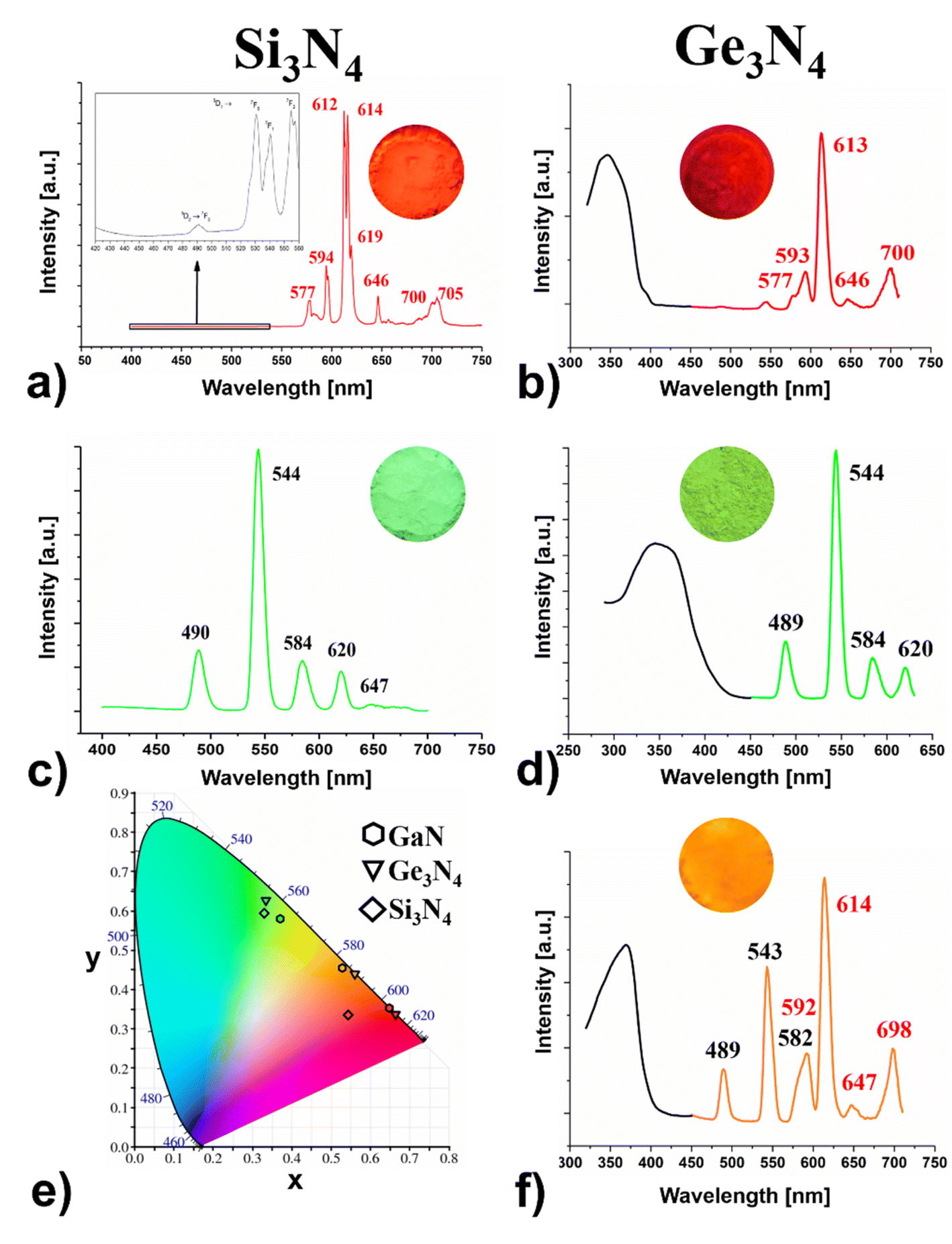 | ||
Fig. 2 Excitation (black) and emission spectra (coloured) of (a) Eu-β-Si3N4 (red, λem = 612/614 nm), (c) Tb-β-Si3N4 (green λem = 544 nm) and of (b) Eu-β-Ge3N4 (red, λem = 613 nm), (d) Tb-β-Ge3N4 (green λem = 544 nm) and (f) Eu- and Tb-β-Ge3N4 (orange λem = 544/614 nm), (e) CIE 1931 diagram of β-Si3N4 (♦), β-Ge3N4 (▼) and GaN (![[hexagon filled, flat-side down]](https://www.rsc.org/images/entities/char_e039.gif) )31,32 adsorbed/doped with Eu, Tb and Eu and Tb. )31,32 adsorbed/doped with Eu, Tb and Eu and Tb. | ||
Taking into account the basics of colour mixing, it is clear that the combination of green and red leads to orange (see Fig. 2f). This effect could be proven in the meantime for other doped nitrides31 e.g., GaN31,32 (see Fig. 2e), and carbodiimides as well.55
Adsorption of β-Si3N4 and β-Ge3N4 with europium
Eu-β-Si3N4 and Eu-β-Ge3N4 show strong characteristic emission peaks of Eu3+ within the region of 570–705 nm, indicating an energy transfer between the β-Si3N4 and β-Ge3N4 hosts and the Eu3+ ions. The peaks associated with the intra-4f shell transitions (5D0 → 7FJ) of the Eu3+ ions, are found at 577, 594, 612, 614, 619, 646 and 700, 705 nm, with those at 612 and 614 nm the most intense ones for β-Si3N4 (see Fig. 2a) whereas for Ge3N4, the corresponding peaks are located at 577, 593, 613 (the most intense), 646 and 700 nm (see Fig. 2b).Fig. 2a shows that in the emission spectrum of Eu-β-Si3N4, the transitions 5D0 → 7F0 and 7F3 seem to be more intense than usually, and the latter is even more pronounced than the 5D0 → 7F4 transition, which is not common. This means a strong J-mixing and a strong crystal-field perturbation might occur in this matrix. The peak corresponding to the 5D0 → 7F0 transition is also broad, indicating the location of Eu3+ ions on several sites in the host structure (see Fig. 2a).
Adsorption of β-Si3N4 and β-Ge3N4 with terbium
The excitation (monitored at 544 nm) and emission spectra of Tb-β-Si3N4 and Tb-β-Ge3N4 are represented in Fig. 2c and d. The excitation spectrum of Tb-β-Si3N4 and Tb-β-Ge3N4 exhibit a broad and intense band in the range from 280 nm to 380 nm with peaks at around 342 and 356 nm, respectively. This broad band is attributed to 4f8 → 4f75d1 transition of the Tb3+ ions. The strongest emission peak is at 544 nm with a full width at half maximum (FWHM) ∼12 nm corresponding to the 5D4 → 7F5 transition, while the peaks at 488, 489 nm, 584 nm and 620 nm originate from the 5D4 → 7F6, 5D4 → 7F4 and 5D4 → 7F3 transitions of the Tb3+ ions, respectively. The green luminescence of Tb-β-Si3N4 and Tb-β-Ge3N4 demonstrates impressively that green emitting phosphors31 can be also achieved with purely nitride compounds and not only with oxynitrides (e.g., β-SiAlON:Eu2+56 or oxonitridosilicates (e.g., SrSi2O2N2:Eu2+57,58 as it was up to now. The energy level distributions of Tb3+ and Eu3+ ions show a large overlap and their energy transfer has been proven to be very effective.59 The blue-green light of the Tb3+ transition (5D4 → 7F6,5) is emitted by polychromatic relaxation and the energy is transferred to the 5D1 and 5D0 levels of the Eu3+ by cross relaxation. The Eu3+ ions absorbing the energy from Tb3+emit therefore orange light.
Fig. 2f–c proves that for Eu,Tb-Ge3N4 two different activator ions can be adsorbed in one host showing the typical bands of Eu3+ as well as the ones of Tb3+ in one spectrum resulting in a saturated orange body colour. However, this is not only a superposition of the Eu3+- and the Tb3+-spectrum of β-Ge3N4 because peak form, intensity and wavelength of this orange spectrum differ clearly in comparison to the spectra of the single doped materials. Therefore, this orange colour is only possible by mixing the ions at an atomic scale and cannot be realized simply by a mixture of particles of the red and the green adsorbed Ge3N4.
To get further evidence powder samples of Eu-Ge3N4 and Tb-Ge3N4 (same molar ratio Eu:Tb as in Eu,Tb-Ge3N4) were mixed in a mortar. This definitely did not result in an orange luminescent β-Ge3N4 sample but a yellow luminescent powder instead (see Fig. S5c and d†). Indeed, compared to a superposition of the Eu- and Tb-spectra, all peaks of the Eu,Tb-β-Ge3N4 spectrum slightly changed in energy and intensity with the peaks resulting from Tb3+ significantly stronger and tuning the colour to the yellow region (CIE coordinates x, y = 0.456, 0.499). This clearly evidenced that the orange body colour (CIE values x, y = 0.559, 0.438) can only be obtained by an atomic scale mixing and that we are able to tune the colour resulting finally in red, green, orange and yellow luminescence for Eu- and Tb-β-Ge3N4. As the mixing at the atomic scale for Eu,Tb-β-Si3N4 was not successful, the combination of the powder samples of equal parts of Eu-β-Si3N4 and Tb-β-Si3N4 was tested. Here we got a completely different result and the CIE diagram shows a saturated orange colour with the coordinates x, y = 0.570, 0.417. (see Fig. S5a and b†). Here we find nearly the same CIE values as the ones of the amber emitting 2-5-8 nitridosilicate phosphor (Ba,Sr)2Si5N8:Eu2+ (x, y = 0.579, 0.416) being considered as an important breakthrough for bridging the “yellow gap”.25
For Eu,Tb-β-Ge3N4 the FWHM pointed out the same value as those of the single doped materials which are in the range of 11–12 nm. This holds true for Tb-β-Si3N4 as well. A much more narrow band is observed for Eu-β-Si3N4 with a FWHM of 2–4 nm. Interestingly, these values are quite smaller than the line widths (FWHM) of the emission spectra of the very narrow-band nitridosilicate phosphors which range between 35–50 nm2 or those of the nitride-based LEDs which vary typically between 20–35 nm.60 The quantum yields were in the range of 5–16%. Tb-β-Si3N4 was 16% and the other compounds around 5%.
To elucidate if the luminescence does not result from the respective rare-earth (RE) compounds and if the Eu and Tb ions really have been adsorbed at the grain boundaries of β-Si3N4 and β-Ge3N4 a comparison of the luminescence spectra of Eu-Si3N4 and Ge3N4 and EuCl3·x6H2O is shown in Fig. S6 and S7.† A comparison between Tb-β-Si3N4 and TbOCl61 is also shown in Fig. S15.† Optical and luminescence spectra are highly sensitive to structural deformation of the nearest environment of RE ions. Therefore, it becomes clearly evident here that the emission spectrum has changed due to the adsorption of the Eu cations into the β-Si3N4 and β-Ge3N4 structures.
A very detailed comparison of our results with those of several Eu- and Tb-Si3N4 thin films and nanowires and possible side products published in the literature was carried out (see ESI Fig. S8–S15† and corresponding section). This indicated that if some luminescence spectra may seem very similar overall at first sight, it turns out that definitely some changes are observed.33–41
DFT calculations
The underlying structure–property relationships in a phosphor, i.e., the relationship between, the nature of the specific atoms, their coordination environment, and the density of states are largely determined by its electronic structure.62 Therefore, DFT calculations were carried out to further elucidate the adsorption of RE ions at the grain boundaries.The β-Si3N4 models were generated in such a way to reproduce the interface observed in high-angle annular dark-field STEM (HAADF-STEM) images of RE doped Si3N4 by Ziegler et al.,63 which evidenced a grain orientated along the [0001] zone axis with the prismatic plane of Si3N4 facing the amorphous intergranular phase. In particular, the rare earth elements have been observed sitting on two atomic sites at the interface, labeled A and B, which are, respectively, small and large open hexagonal rings Fig. 3.
 | ||
| Fig. 3 Relaxed atomic structure for the models used to describe the β-Si3N4 grain interface with RE elements (Eu or Tb) at the A-site (a) and B-site (b). Nitrogen, oxygen, hydrogen and RE atoms are represented in blue, red, white and purple, respectively. | ||
Note that the creation of the interface led to dangling bonds, which were passivated using both O2− and N3− ions, in order to respect the electroneutrality of the unit cell. For both Eu and Tb ions on sites A and B, atomic coordinates were relaxed leading systematically to a higher stability when the rare earth resides on site A (highly coordinated) than on site B, with an energy difference of 745 and 851 meV per rare earth for Eu3+ and Tb3+, respectively.
For the more stable interface, i.e., with the rare earth located on site A, simulations of the Si L23 edge were performed for silicon atoms close to the interface in order to probe both their location and chemical environment. Indeed, precise electron energy loss spectroscopy (EELS) measurements were reported for RE doped Si3N4 ceramics,63 allowing us to compare our model with experimental data. Such a simulation required to properly treat the electron–hole interaction (excitonic effects) using Bethe–Salpeter equations for instance. Here, due to the size of the system, we chose to consider this electron–hole Coulomb interaction as a static screening using the core–hole approximation. More precisely, half an electron was removed from a core orbital, i.e., the Slater's transition state.64 For the doped Tb-β-Si3N4 model, the core-hole was introduced in the 2p1/2 and 2p3/2 states of the excited silicon atoms. The simulation is thus a summation of two spectra resulting from two static calculations with, respectively, half a core-hole in 2p1/2 and 2p3/2 states of the probed silicon atoms. In order to validate such a static screening approximation, the related bulk system Si2N2O was simulated and compared to experiments63 (see Fig. 4a). A good agreement is observed, with a small discrepancy around 104 eV both in terms of peak position and intensity. Such an agreement confirms that the Slater's transition state allows to properly describe the Si L23 edge of silicon atoms surrounded by nitrogen and oxygen atoms.
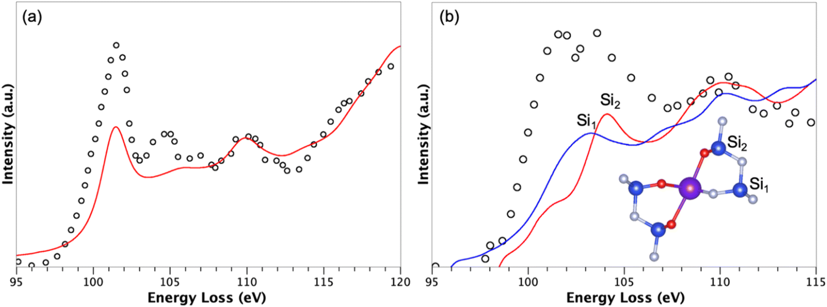 | ||
| Fig. 4 Simulated Si L23 EELS data (red and blue lines) compared to measurements (open circles) from ref. 63 of (a) Si2N2O and (b) the adsorbed Tb-β-Si3N4 model with Tb ions on A site. The simulations have been done using the Slater's transition state. For the interface, two simulations have been done for one silicon atom surrounded by N3− ions only, and one silicon atom with O2− ions in its first coordination sphere. | ||
Fig. 4b shows two simulations corresponding to Si L23 edge of two silicon atoms nearby the interface with Tb ions on site A. One silicon atom, labeled Si1 (Fig. 4b) is surrounded only by nitrogen atoms while the other one, labeled Si2 (Fig. 4b) is environed by oxygen and nitrogen atoms. Note that the experimental spectrum (open circles) related to site A is characterized by a double peak (102 and 103.5 eV), with a first peak assigned to Si–N bonds and the second one to Si–O bonds. Interestingly, our simulations evidenced a peak at 103 eV for Si1 and 104.1 eV for Si2, confirming the previous interpretation and validating the model used to mimic locally the interface in the grain boundary region.
DFT + U + SOC calculations were then carried out on the adsorbed Tb-β-Si3N4 model considering the previously optimized atomic structures. Such calculations were indeed not trivial and could be difficult to converge when the ground state is close in energy to other magnetic states. The convergence of these calculations was achieved only for the Tb compounds. Spin (orbital) moments of 6.03 (1.45) and 6.04 (2.73) μB were computed for Tb ions on sites A and B, respectively, leading to total magnetic moments of 7.48 and 8.77 μB, respectively. These values are somewhat smaller than the theoretical value of 9 μB expected for a free Tb3+ ion. This is due to the crystalline field of the surrounding ligands which is stronger for Tb ions on site A than on site B. On site A, the most energetically preferred site of Tb is positioned in an octahedral environment, while on site B, Tb is sitting in a too large site, which creates a less intense crystalline field. This explains the weaker moment value, in particular the orbital moment of the former with respect to the latter.
Fig. 5 shows the densities of states (DOS) obtained with Tb3+ atoms on A and B sites computed at the DFT + U + SOC level of theory. The valence band (VB), from −12 to 0 eV, is mainly based on N 2p states interacting with Si(3p) states. The O 2p states of the interface appears in the VB from −10 to −2 eV. The conduction band, starting at 2 eV, is mainly composed of Si 3p states interacting with N 2p states. The band gap is only 2 eV in both cases. For comparison, the DFT estimated band gap of β-Si3N4 was 4.2 eV. The decrease in the band gap value is indeed the consequence to additional interactions involving the Tb 5d states found both at the top of the VB and the bottom of the conduction band (CB) (see Fig. 5).
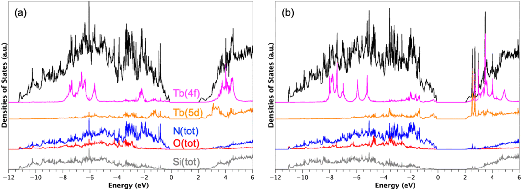 | ||
| Fig. 5 Densities of states (DOS) calculated with Tb atoms on site A (a) and on site B (b). The Fermi level was defined as the reference of energies (EF = 0 eV). The total DOS is represented in black and the projected DOS in colours. The calculations were carried out at the DFT + U + SOC level of theory, i.e., with Ueff = U − J = 6 eV for the 4f states of the rare-earth element and including spin-orbit coupling (SOC). | ||
Such a band gap reduction was already discussed by Huang et al.40 for Y-doped Si3N4, due to Y 4d states. These reduced band gaps are directly responsible for the luminescent properties of the adsorbed RE-β-Si3N4 (RE = Eu, Tb) materials.
Mott–Schottky (MS) measurements
The emission colour of a phosphor strongly depends on the nature of the incorporated activator, the host material and its electronic configuration.65–68 Electrochemical impedance spectroscopy (EIS) is an appropriate tool to study ion diffusion and to resolve the chemical identity of the charge carriers by the use of blocking electrodes. Mott–Schottky (MS) measurements are very sensitive to probe changes in the electronic band structure, i.e. charge carrier density, type of semiconducting behaviour and band edge positions, upon adsorbing. For the elucidation of the adsorbing effect on the electronic properties of Si3N4 and Ge3N4, MS measurements were conducted for the bare and RE adsorbed samples. They were performed in a 0.1 M potassium phosphate electrolyte (pH 7) in the dark with a setting at ac amplitude of 5 mV and at an applied frequency of 10 and 100 Hz (see Fig. S16 and S17†). As shown in Fig. 6, all of the acquired curves show a positive slope corresponding to the characteristic of n-type semiconductors, indicating that bare and RE adsorbed materials of β-Si3N4 and β-Ge3N4 are n-type semiconductors.69 In addition, a smaller slope for all curves can be attributed to increased charge carrier density for Si3N4 upon adsorbing with the rare-earth metals.70,71 The extrapolation of the curves allows to estimate the flat band potential as the corresponding conduction band edge of n-type semiconductors. A comparison of the results obtained from these plots in Fig. 6 reveals that the obtained conduction band edges of RE adsorbed Si3N4 and Ge3N4 yield a significant shift, indicating that RE adsorbing can be applied to modify the (photo)electrochemical properties of Si3N4 and Ge3N4.71–73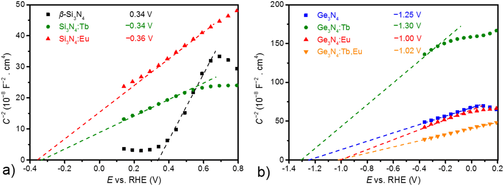 | ||
| Fig. 6 MS analysis of EIS measurements of (a) pure Si3N4 (black), Tb-Si3N4 (green), Eu-Si3N4 (red) and (b) pure Ge3N4 (blue), Tb-Ge3N4 (green), Eu-Ge3N4 (red) and Eu,Tb-Ge3N4 (orange). Measurements were performed in a 0.1 M potassium phosphate electrolyte at pH 7, at an applied frequency of 100 Hz for (a) and an applied frequency of 1000 Hz for (b). The extrapolated curves at y = 0 correspond to the conduction band edges, because the materials exhibit a positive slope that is characteristic for an n-type semiconductor. The determined flatband potentials are provided in the inset. | ||
Conclusions
The successful adsorption of bulk β-Si3N4 and β-Ge3N4 with Eu and Tb and the synergic combination of both resulted in intriguing luminescence properties of all adsorbed compounds (red, green, orange and yellow). The theoretical and experimental results strongly highlight the opportunities for controlling functionality and luminescence properties of modern energy-efficient white light-emitting diodes.Especially, the fact that one host can deliver different colours renders Eu,Tb-Si3N4 and Eu,Tb-β-Ge3N4 as prospective chief components for future light emitting diodes (LEDs). Not only several colours could indeed be realized by an atomic scale mixing, but the colour could also be tuned by mixing the adsorbed hosts enlarging the colour range with red, green, orange and yellow luminescence for the extremely narrow-band Eu- and Tb-M3N4 materials (M = Si, Ge). It could be shown that the realization of an amber emitting phosphor for both, Si3N4 and Ge3N4, is possible.
This work also studied the types and the flat band edges of β-Si3N4 and β-Ge3N4 before and after adsorption with RE materials were also studied in this work. A detailed physical characterization by MS analysis of EIS revealed that a significant shift of the flat band edge was observed caused by the adsorbing with Eu and Tb ions. This can be seen as a complementary strategy to modify the band edge of materials. Moreover, this could be applicable to photoelectrodes used to adapt and optimize (photo)electrochemical performances.
Experimental section
Adsorption of Si3N4 and Ge3N4
The adsorption of β-Si3N4 (Chempur 99999%) and β-Ge3N4 (VWR 9999%) was realized by a successive combustion synthesis in combination with the respective metal chlorides (MCl3·6H2O or M(NO3)3·5H2O (M = Eu, Tb), NH4NO3, urea and H2O. This mixture was put into an oven for 10 min at 400–600°. The RE content, which is about 3–5 at%, -has been checked via EDX measurements.
X-ray diffraction
X-ray diffraction experiments on Si3N4- and Ge3N4-based powder samples were performed on a STOE STADI P powder diffractometer in Debye–Scherrer geometry with Ge (111)-monochromatized Mo-Kα1 radiation (λ = 0.709026 Å). The samples were enclosed in a glass capillary of 0.3 mm diameter.EDX measurements
SEM was performed on a Zeiss Merlin microscope and for EDX we used a Quantax 400 system from Bruker.Mott–Schottky (MS) measurements
Electrodes fabrication
Si3N4 and Ge3N4 and the corresponding rare-earth metal (RE = Eu, Tb and Eu/Tb) adsorbed semiconductor electrodes were prepared by electrophoretic deposition. Fluorine doped tin oxide (FTO) glass (2.2 mm thick, Sigma-Aldrich) was used as the substrate after sequentially ultrasonic cleaning with dilute nitric acid, acetone and ethanol for 15 min. The dispersion was prepared by mixing 5 mg iodine and 20 mg sample with 20 ml acetone, followed by treatment with ultrasounds. The electrodes were obtained after depositing the dispersed powder at 30 V and drying under ambient atmosphere.Mott–Schottky (MS) measurements
The MS measurements were performed in an electrochemical cell using a potentiostat (Gamry instruments) operating in a three-electrode setup. The deposited samples on FTO, a 1 M Ag/AgCl electrode and a platinum wire were used as a working electrode, a reference electrode and a counter electrode, respectively. All MS data were recorded vs. E1 M Ag/AgCl (V), which was subsequently converted with respect to ERHE (V) according to the formula: ERHE (V) = 0.235 + E1 M Ag/AgCl + [0.059 × pH] (V) at 25 °C.Luminescence
The luminescence spectra and quantum yield measurements were performed on a Fluorolog®-3 Horiba Jobin Yvon equipped with a TBX detector picosecond photon detection device and a 450 W xenon lamp.DFT calculations
Density functional theory (DFT) calculations were carried out on pure and adsorbed β-Si3N4 and β-Ge3N4. See ESI for the computational details.†Author contributions
Dr Cordula Braun: concept, coordination, synthesis, luminescence investigations, writing and editing of the manuscript. Liuda Mereacre: technical help and support with synthesis investigations. D. Vincent: performed the theoretical calculations and interpreted the results. Prof. Dr X. Rocquefelte and Prof. Dr J.-F. Halet: analysed the computational data and participated to the writing and editing of the respective part of the manuscript. Prof. Dr Adam Slabon: designed the photochemical experiments (Mott–Schottky measurements) and wrote the photochemical part. Zheng Chen: performed the EIS and photochemical experiments.Conflicts of interest
There are no conflicts of interest.Acknowledgements
The authors gratefully acknowledge Udo Geckle (IAM-ESS KIT Karlsruhe) for the EDX and Sabine Schlabach (INT KIT Karlsruhe) for luminescence measurements. Furthermore we acknowledge support by the KIT-Publication Fund of the Karlsruhe Institute of Technology.References
- P. Ball, Nat. Mater., 2015, 14, 453 CrossRef PubMed.
- P. Pust, P. J. Schmidt and W. Schnick, Nat. Mater., 2015, 14, 454–458 CrossRef CAS PubMed.
- S. Nakamura, Angew. Chem., Int. Ed., 2015, 54, 7770–7788 CrossRef CAS PubMed.
- I. Akasaki, Angew. Chem., Int. Ed., 2015, 54, 7750–7763 CrossRef CAS PubMed.
- H. Amano, Angew. Chem., Int. Ed., 2015, 54, 7764–7769 CrossRef CAS PubMed.
- M. Zeuner, S. Pagano and W. Schnick, Angew. Chem., Int. Ed., 2011, 50, 7754–7775 CrossRef CAS PubMed.
- H. Lange, G. Wötting and G. Winter, Angew. Chem., Int. Ed., 1991, 30, 1579–1597 CrossRef.
- C. Braun, Doctoral thesis, Ludwig-Maximilians-Universität München, 2010.
- S. R. Römer, C. Braun, O. Oeckler, P. J. Schmidt, P. Kroll and W. Schnick, Chem.–Eur. J., 2008, 14, 7892–7902 CrossRef PubMed.
- T. Jüstel, H. Nikol and C. Ronda, Angew. Chem., Int. Ed., 1998, 37, 3084–3103 CrossRef.
- Luminescence, ed. C. Ronda, Wiley-VCH Verlag GmbH & Co. KGaA, Weinheim, Germany, 2007 Search PubMed.
- W. Schnick, Phys. Status Solidi, 2009, 3, 1–2 Search PubMed.
- P. Schmidt, A. Tuecks, J. Meyer, H. Bechtel, D. Wiechert, R. Mueller-Mach, G. Mueller and W. Schnick, Seventh Int. Conf. Solid State Light., 2007, 6669, P6690 Search PubMed.
- K. Uheda, K. Uheda, S. Shimooka, S. Shimooka, M. Mikami, M. Mikami, H. Imura, H. Imura, N. Kijima and N. Kijima, Sci. Technol., 2007, 899–902 Search PubMed.
- L. Gamperl, P. Strobel, P. J. Schmidt and W. Schnick, Chem.–Eur. J., 2022, e202200760 CAS.
- R. Shafei, D. Maganas, P. J. Strobel, P. J. Schmidt, W. Schnick and F. Neese, J. Am. Chem. Soc., 2022, 144, 8038–8053 CrossRef CAS PubMed.
- T. De Boer, T. D. Boyko, C. Braun, W. Schnick and A. Moewes, Int. J. Appl. Ceram. Technol., 2022, 1–7 CAS.
- C. Braun, M. Seibald, S. L. Börger, O. Oeckler, T. D. Boyko, A. Moewes, G. Miehe, A. Tücks and W. Schnick, Chem.–Eur. J., 2010, 16, 9646–9657 CrossRef CAS PubMed.
- C. Braun, S. L. Börger, T. D. Boyko, G. Miehe, H. Ehrenberg, P. Höhn, A. Moewes and W. Schnick, J. Am. Chem. Soc., 2011, 133, 4307–4315 CrossRef CAS PubMed.
- C. Braun, H. Ehrenberg and W. Schnick, Eur. J. Inorg. Chem., 2012, 2012, 3923–3928 CrossRef CAS.
- R. Mueller-Mach, G. Mueller, M. R. Krames, H. A. Höppe, F. Stadler, W. Schnick, T. Juestel and P. Schmidt, Phys. Status Solidi A, 2005, 202, 1727–1732 CrossRef CAS.
- Y. Q. Li, G. de With and H. T. Hintzen, J. Mater. Chem., 2005, 15, 4492–4496 RSC.
- X. Piao, T. Horikawa, H. Hanzawa and K. Machida, Appl. Phys. Lett., 2006, 88, 161908 CrossRef.
- R. J. Xie, N. Hirosaki, Y. Li and T. Takeda, Materials, 2010, 3, 3777–3793 CrossRef CAS.
- R. Mueller-Mach, G. O. Mueller, M. R. Krames, O. B. Shchekin, P. J. Schmidt, H. Bechtel, C. H. Chen and O. Steigelmann, Phys. Status Solidi, 2009, 3, 215–217 CAS.
- S. Schmiechen, H. Schneider, P. Wagatha, C. Hecht, P. J. Schmidt and W. Schnick, Chem. Mater., 2014, 26, 2712–2719 CrossRef CAS.
- S. Schmiechen, P. Pust, P. J. Schmidt and W. Schnick, Nachr. Chem., 2014, 62, 847–851 CrossRef CAS.
- P. Pust, F. Hintze, C. Hecht, V. Weiler, A. Locher, D. Zitnanska, S. Harm, D. Wiechert, P. J. Schmidt and W. Schnick, Chem. Mater., 2014, 26, 6113–6119 CrossRef CAS.
- P. Pust, V. Weiler, C. Hecht, A. Tücks, A. S. Wochnik, A.-K. Henß, D. Wiechert, C. Scheu, P. J. Schmidt and W. Schnick, Nat. Mater., 2014, 139, 891–896 CrossRef PubMed.
- E. Elzer, P. Strobel, V. Weiler, P. J. Schmidt and W. Schnick, Chem. Mater., 2020, 32, 6611–6617 CrossRef CAS.
- C. Braun, Bulk materials of doped multinary nitrides and nitridosilicates, their production method and uses, EP20186968, 2020.
- C. Braun, L. Mereacre, Z. Chen and A. Slabon, Sci. Rep., 2022, 12, 1–7 CrossRef PubMed.
- Y. Q. Li, N. Hirosaki, R. J. Xie, T. Takeda and M. Mitomo, J. Lumin., 2010, 130, 1147–1153 CrossRef CAS.
- Q. Li, C. Gong, X. Cheng and Y. Zhang, Ceram. Int., 2015, 41, 4227–4230 CrossRef CAS.
- Z. Huang, Z. Wang, H. Yuan, J. Zhang, F. Chen, Q. Shen and L. Zhang, J. Mater. Sci., 2018, 53, 13573–13583 CrossRef CAS.
- L.-W. Yin, Y. Bando, Y.-C. Zhu and Y.-B. Li, Appl. Phys. Lett., 2003, 83, 3584–3586 CrossRef CAS.
- R. Su, Z. F. Huang, F. Chen, Q. Shen and L. M. Zhang, Key Engineering Materials, Trans Tech Publications Ltd., 2017, vol. 727, pp. 635–641 Search PubMed.
- X. Xu, T. Nishimura, Q. Huang, R.-J. Xie, N. Hirosaki and H. Tanaka, J. Am. Ceram. Soc., 2007, 90, 4047–4049 CAS.
- Z. Huang, F. Chen, Q. Shen and L. Zhang, RSC Adv., 2016, 6, 7568–7574 RSC.
- Z. Huang, F. Chen, R. Su, Z. Wang, J. Li, Q. Shen and L. Zhang, J. Alloys Compd., 2015, 637, 376–381 CrossRef CAS.
- Z. Huang, R. Su, H. Yuan, J. Zhang, F. Chen, Q. Shen and L. Zhang, Ceram. Int., 2018, 44, 10858–10862 CrossRef CAS.
- N. Liu, J. Zhang, Y. Duan, X. Li and S. Dong, J. Eur. Ceram. Soc., 2020, 40, 1132–1138 CrossRef CAS.
- P. F. Becher, G. S. Painter, N. Shibata, S. B. Waters and H.-T. Lin, J. Am. Ceram. Soc., 2008, 91, 2328–2336 CrossRef CAS.
- G. S. Painter, F. W. Averill, P. F. Becher, N. Shibata, K. Van Benthem and S. J. Pennycook, Phys. Rev. B: Condens. Matter Mater. Phys., 2008, 78, 214206 CrossRef.
- G. S. Painter, P. F. Becher, W. A. Shelton, R. L. Satet and M. J. Hoffmann, Phys. Rev. B: Condens. Matter Mater. Phys., 2004, 70, 144108 CrossRef.
- G. S. Painter, R. L. Satet, M. J. Hoffmann, S. J. Pennycook and P. F. Becher, Phys. Rev. B: Condens. Matter Mater. Phys., 2005, 72, 140101 CrossRef.
- H. Gu, X. Pan, R. M. Cannon and M. Rühle, J. Am. Ceram. Soc., 1998, 81, 3125–3135 CrossRef CAS.
- H. Hayashi, K. Hirao, M. Toriyama, S. Kanzaki and K. Itatani, J. Am. Ceram. Soc., 2001, 84, 3060–3062 CrossRef CAS.
- N. Shibata, S. J. Pennycook, T. R. Gosnell, G. S. Painter, W. A. Shelton and P. F. Becher, Nature, 2004, 428, 730–733 CrossRef CAS PubMed.
- J. a. Kechele, O. Oeckler, F. Stadler and W. Schnick, Solid State Sci., 2009, 11, 537–543 CrossRef CAS.
- S. Shimooka, K. Uheda, M. Mikami, N. Kijima, H. Imura and K. Horibe, WO088966, 2007.
- Y. Q. Li, G. De With and H. T. Hintzen, J. Electrochem. Soc., 2006, 153, G278–G282 CrossRef CAS.
- Y. Q. Li, G. de With and H. T. Hintzen, J. Alloys Compd., 2004, 385, 1–11 CrossRef CAS.
- M. J. Hoffmann, personal message, 2020.
- C. Braun, L. Mereacre, W. Hua, T. Stürzer, I. Ponomarev, P. Kroll, A. Slabon, Z. Chen, Y. Damour, X. Rocquefelte, J. Halet and S. Indris, ChemElectroChem, 2020, 7, 4550–4561 CrossRef CAS.
- D. H. Kim, J. H. Ryu and S. Y. Cho, Appl. Phys. A: Mater. Sci. Process., 2011, 102, 79–83 CrossRef CAS.
- Y. Q. Li, A. C. A. Delsing, G. De With and H. T. Hintzen, Chem. Mater., 2005, 17, 3242–3248 CrossRef CAS.
- V. Bachmann, T. Jüstel, A. Meijerink, C. Ronda and P. J. Schmidt, J. Lumin., 2006, 121, 441–449 CrossRef CAS.
- D. Halmurat, T. Yusufu, Q. Wang, J. He and A. Sidike, Sci. Rep., 2019, 9, 14637 CrossRef PubMed.
- R. Mueller-Mach and G. O. Mueller, Proc. SPIE, 2000, 3938, 30–41 CrossRef CAS.
- P. A. M. Berdowski, J. van Herk, L. Jansen and G. Blasse, Phys. Status Solidi, 1984, 125, 387–391 CrossRef CAS.
- P. Dorenbos, J. Mater. Chem., 2012, 22, 22344–22349 RSC.
- A. Ziegler, J. C. Idrobo, M. K. Cinibulk, C. Kisielowski, N. D. Browning and R. O. Ritchie, Science, 2004, 306(5702), 1768–1770 CrossRef CAS PubMed.
- T. Mizoguchi and I. Tanaka, Phys. Rev. B: Condens. Matter Mater. Phys., 2000, 61, 2180–2187 CrossRef CAS.
- T. M. Tolhurst, P. Strobel, P. J. Schmidt, W. Schnick and A. Moewes, Chem. Mater., 2017, 29, 7976–7983 CrossRef CAS.
- M. R. Amin, P. Strobel, A. Qamar, T. Giftthaler, W. Schnick and A. Moewes, Adv. Opt. Mater., 2020, 8, 2000504 CrossRef CAS.
- T. de Boer, T. D. Boyko, C. Braun, W. Schnick and A. Moewes, Phys. Status Solidi RRL, 2015, 9, 250–254 CrossRef CAS.
- M. R. Amin, E. Elzer, W. Schnick and A. Moewes, J. Phys. Chem. C, 2021, 125, 11828–11837 CrossRef CAS.
- A. Lasia, in Electrochemical Impedance Spectroscopy and Its Applications, Springer New York, New York, NY, 2014, pp. 251–255 Search PubMed.
- R. O'Hayre, M. Nanu, J. Schoonman and A. Goossens, J. Phys. Chem. C, 2007, 111, 4809–4814 CrossRef.
- K. Gelderman, L. Lee and S. W. Donne, J. Chem. Educ., 2007, 84, 685–688 CrossRef CAS.
- B. Iandolo, H. Zhang, B. Wickman, I. Zorić, G. Conibeer and A. Hellman, RSC Adv., 2015, 5, 61021–61030 RSC.
- D. W. Hwang, J. Kim, T. J. Park and J. S. Lee, Catal. Lett., 2002, 80, 53–57 CrossRef CAS.
Footnote |
| † Electronic supplementary information (ESI) available. See DOI: https://doi.org/10.1039/d2ra04663f |
| This journal is © The Royal Society of Chemistry 2022 |