
 Open Access Article
 This Open Access Article is licensed under a Creative Commons Attribution-Non Commercial 3.0 Unported Licence
Fabrication of Cu@Sn TLPS joint for high temperature power electronics application
Honghui Zhanga,
Hongyan Xu *b,
Xuan Liub and
Ju Xub
*b,
Xuan Liub and
Ju Xub
aXinyang Vocational and Technical College, Xinyang, 464000, China. E-mail: zhh20080115@163.com
bMicro-nano Fabrication Technology Department, Institute of Electronic Engineering, Chinese Academy of Sciences, Beijing, 100190, China. E-mail: hyxu@mail.iee.ac.cn
First published on 12th October 2022
Abstract
In this study, a novel Cu@Sn TLPS joint was fabricated for high-temperature power electronics application. Cu@Sn core–shell composite powder was firstly prepared by a methylate electroplating method, and then pressed into a preformed sheet. The Cu@Sn preform was reflowed at 250 ∼ 280 °C for 40 min under the pressure of 0.1 × 10⁻³ MPa, and the resulting bondline can withstand high temperatures up to 600 °C. During the process, the Sn layer was transformed to Cu3Sn, and the Cu3Sn surrounded the outside of the residual Cu particles. The joint characteristics were controlled by size gradation of Cu particles, the ratio of Cu/Sn, preform forming pressure and TLPS process. The joint shear strength was no less than 48 MPa after aging at 400 °C for 1000 h. Young's modulus and hardness were 98.35 GPa and 2.62 GPa, respectively, which are much lower than the pure Cu3Sn joint. The electrical resistivity and thermal conductivity of the joint were 5.1 μΩ cm and 148 W m−1 K−1, respectively. It is superior to pure Cu3Sn joints and the other Cu/Sn system TLPS joints. The high shear strength, high thermal conductivity and high melting temperature demonstrate that Cu@Sn TLPS joint is a promising interconnect technology for high power density modules.
Introduction
New generation wide-band semiconductor devices can improve the operating temperature and power density, which show greater potential for high-temperature applications.1,2 However, the increasing operating temperature, the harsh environment, increased instability, and other safety problems become great challenges for the corresponding high-temperature resistant bonding materials and joint reliability. The traditional high lead alloy, Au–Sn, and other eutectic alloy solders can easily lead to chip warpage deformation under high process temperature, and they are unable to meet the needs of higher service temperature for SiC devices. Although sintered nano-silver shows high comprehensive performance, due to the existence of electromigration, the welding process requires high pressure and high cost, making it difficult to be a popular application. Transient liquid phase bonding (TLPB) has the characteristics of both fusion and diffusion welding, which can be achieved at low processing temperatures and obtained higher remelting temperatures. Kunmo Chu et al.3 applied the sandwiched Cu/Sn/Cu and Ni/Sn/Ni structure material TLPS to prepare pure interfacial intermetallic compound (IMCs) joints. This sandwiched structure is based on an interfacial layer of low-melting-point metals, such as Sn, In, and a surface layer of high-melting-point metals, such as Cu, Ni, Ag, and other metals.4–6 The liquid–solid interdiffusion is used to generate high temperature resistant IMCs as the interconnecting joint, but the disadvantages are also distinguished: the long diffusion channel of Cu/Sn/Cu structure, thus weakening the reaction kinetics; the difficulty to extend the interface layer thickness; besides, pure IMCS joints increase the elastic modulus, while reducing the fracture toughness, which are not conducive to reliable operation at high temperatures.A composite powder-based TLPB technology for the preparation of IMCs high-temperature joints has attracted a lot of attention.7–9 The advantage of this technique is that the Cu/Sn particles are uniformly mixed and fully inter-contacted, the molten Sn completely infiltrates the Cu particles, which greatly shortens the diffusion channel and strengthens the reaction kinetics, and after a certain time, the isothermal diffusion alloying reaction generates a homogeneous Cu6Sn5/Cu3Sn compound. Hannes Greve et al. successfully prepared complete Cu6Sn5 and Cu3Sn joints with a joint thickness of less than 10 μm, and the thermoelectricity properties of the joint can be comparable to those of pure silver.10 A. Syed-Khaja et al. prepared large-area, cavity-free Cu6Sn5 and Cu3Sn joints with 15 ∼ 20 μm thickness layer by using vacuum soldering or high-pressure soldering techniques for Cu–Sn solder paste. Through process optimization, high-temperature resistant joints were prepared on conventional welding equipment, and the joints had remelting temperatures higher than 400 °C and excellent thermoelectric properties.11 The structure of the above prepared high-temperature resistant joints is still pure IMCs phase, though the thermoelectric property is enhanced, but the high elastic modulus and susceptibility to brittle fracture at the joint interface have not been solved yet. Therefore, the joint structure needs to be improved to strengthen the toughness of the joint.
The Cu6Sn5/Cu3Sn joints composed of pure intermetallic compounds have high elastic modulus (about 117∼135 GPa), and insufficient toughness, which is not beneficial to the stable and reliable operation at harsh environment. Due to Young's modulus of Cu being 90 ∼ 110 GPa, which is lower than that of Cu/Sn IMCs, doping Cu in the Cu6Sn5/Cu3Sn joint structure could help improve the toughness of the joints. The SnAgCu/Cu system used in the traditional electronic packaging has an interface composition of Cu6Sn5/Cu3Sn/Cu with a shear strength of 100 MPa.12 Christian Ehrhardt et al. used a secondary TLPB process based on Cu–Sn (Sn-based alloy) solder paste to reduce the oxidation of the particles and the interfacial void rate to obtain co-distributed joints of Cu6Sn5/Cu3Sn with Cu particles, which greatly improved toughness, strength and fatigue life.13
In this paper, Cu@Sn core–shell structure composite powder-transient liquid phase diffusion soldering (TLPS) technology for high-temperature resistant power packaging was studied. The Cu@Cu3Sn joint characteristics were optimized by controlling size gradations of Cu, the ratio of Cu/Sn, preform pressure and TLPS process. Joint properties and failure behavior were mainly studied in this paper.
Materials and methods
Preparation of Cu@Sn composite powders
Copper powder (Grinm Group Corporation Limited, Beijing, China) with different particle size gradations of <15 μm, 15 ∼ 25 μm and 25 ∼ 50 μm were selected and uniformly plated with <1 ∼ 2 μm, 2 ∼ 3 μm and 3 ∼ 5 μm-thick Sn layer, respectively. Cu particles were pretreated with ethanol and hydrochloric acid solution for the removal of the organic impurities and oxide layer, respectively. The activated powder was cleaned with ethanol and deionized water for 3 to 5 times. The different size of copper powder was then electroplated in prepared solution which contained stannous methyl sulfonic acid, methyl sulfonic acid, resorcinol, emulsifier and deionized water, uniformly dense Sn layer was prepared by DC pulse-intermittent stirring, the current density (0.1 ∼ 0.25 A), duty ratio is 1/3 ∼ 1/4, the Sn coating layer thickness was controlled by electroplated time (2 ∼ 4 min) and stirring ratio (30–50 rpm). The prepared Cu@Sn core–shell powder was cleaned by distilled water and ethanol for five times before dried in oven. Finally, different size gradations of Cu@Sn particles of <15 μm, 15 ∼ 25 μm and 25 ∼ 50 μm were mixed in proportion of 1![[thin space (1/6-em)]](https://www.rsc.org/images/entities/char_2009.gif) :3:2.
:3:2.
Preparation and Characteristics Analysis of Bonding Sample
The above prepared Cu@Sn powders were pressed into preform sheets with φ 9 mm × 100 μm under a pressure of 10 MPa for 5 min. The chip scale package with Cu@Sn preform sheet was placed onto Al2O3 ceramic substrate direct bonding copper (DBC) and soldered on a single-zone reflowing oven. The component metalized layer on the DBC substrate is a 1 ∼ 2 μm electroplated Sn layer. The schematic configuration of the preform and joint was shown in Fig. 1. The assemblies were reflowed using the temperature profile which was optimized in our previous work (see Fig. 2). | ||
| Fig. 1 Schematic of the fabrication process of the preform and joint. | ||
 | ||
| Fig. 2 Temperature profile of Cu@Sn preform. | ||
Samples were then reflowed isothermally in oven at 250, 280 and 310 °C, respectively, with different periods of 500, 1000, 1500, and 2000 seconds. Specimens are cross-sectioned through solder joints to observe metallographic features. The mean thickness of the intermetallic layer was measured by using a powerful image processing system, OPTIMAS, together with a Nikon optical microscope. The mean of 6 readings was taken at different locations on each of the three solders. The micro structural details of the joints interface were observed by using a Scanning electron microscope (Philips XL40) and X-ray diffraction (XRD, Philips X’ Pert system).
The XRD was used to show the patterns of the core–shell Cu@Sn powder and soldering samples. The electrical resistivity of the preform after reflow at 280 °C for 40 min was measured using the Seebeck coefficient tester (CTA). The thermal conductivity of the preform was obtained by the laser flash apparatus (LFA) and differential scanning calorimetry (DSC). Nano-indentation testing was carried out on TLPS preform at least 10 times at different locations using the nano-indenter with a pyramid tip. The shear strength of the joint was evaluated by a shear tester at head speed of 1 mm min−1. All the above measurement technologies have been introduced by our previous works.14–16
Results and discussion
Composition and microstructure of Cu@Sn particles and joint bulk
Surface and cross-section morphology of the prepared Cu@Sn core–shell composite powder is illustrated in Fig. 3a and 3b. Combined with the line-scanning results, as shown in Fig. 3c, it can be seen that the surface is uniformly coated with an Sn layer, and the microscope images of the cross-sections of the powder indicate that the thickness of the Sn layer is about 1 ∼ 3 μm. The Sn element gradually decreases to 0% and the Cu element gradually increases to 100% along from the outer shell to inter-core.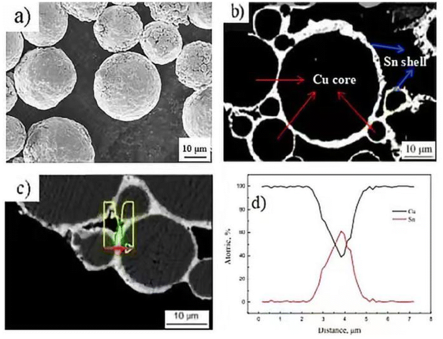 | ||
| Fig. 3 (a) Surface morphology, (b) and (c) profile morphology, (d) profile EDS results of Cu@Sn core–shell structure powder. | ||
The microstructure and composition evolution of the Cu@Sn preform reflowed at 280 °C for different holding times were analyzed. As shown in Fig. 4a), there is residual Sn in the interface when reflowing time is 30 s, and the IMC phase is mainly Cu6Sn5. With the extension of isothermal alloying time, Cu diffuses to Cu6Sn5 through Cu3Sn, and Cu6Sn5 reacts with Cu to form more Cu3Sn. When heat preservation lasted for 60 s (Fig. 4b), Sn was completely consumed and a small amount of Cu3Sn was generated in the interface near the Cu side. As shown in Fig. 4c), there was still Cu6Sn5 in the interface after isothermal holding for 1200 s, the Cu3Sn was formed at expense of Cu6Sn5 and Cu particles. In the area where the copper particle size is not well matched, a thicker Cu6Sn5 phase will be formed, and the ratio of the amount of substance reacts with copper is 9:1. Due to the high density of Cu3Sn phase, volume contraction occurs when Cu6Sn5 was transformed to Cu3Sn, resulting in cavities at the interface of IMCs, as shown in Fig. 4c and d.
 | ||
| Fig. 4 Microstructure of the interface of the Cu@Sn preform after heating at 280 °C for (a) 30 s, (b) 60 s, (c) and d) 1200 s, respectively. | ||
According to XRD results of Cu@Sn preform (seen in Fig. 5), when the reaction time is more than 5 min, Cu6Sn5 can be detected at the soldering interface. The peak of Cu6Sn5 did not disappear completely at the reaction time of 80 min, indicating that the complete transformation of Cu6Sn5 to Cu3Sn was not completed, which was consistent with the SEM results above. In the microstructure, different size gradated Cu particles coated by Cu3Sn and Cu6Sn5 phase are evenly distributed in the bulk.
 | ||
| Fig. 5 XRD results of Cu@Sn preform after heating at 280 °C for different holding time. Interfacial Structure Analysis of Cu@Sn Preform/DBC Substrate. | ||
In order to fill the roughness between the substrate and the preform during TLPS process, a layer of metal was electroplated or sputtered on the substrate. If the coating metal is Sn, the liquid phase amount in the TLPS reaction process can be increased at the same time. The substrate is pretreated with the same process as electroplating powder, and a layer of dense Sn of about 2 μm was evenly spread on the substrate, as shown in Fig. 6a).
 | ||
| Fig. 6 DBC substrate with (a) Sn coating and (b) Ag coating. | ||
The interfacial poor welding quality caused by non-coplanar the substrate and the Cu@Sn preform is effectively improved. The microstructure of the whole joint is uniform, and there is no defect in a large area, the interfacial microstructure of Cu@Sn TLPS joint was shown in Fig. 7.
 | ||
| Fig. 7 SEM image of interface of DBC (Sn coating)/Cu@Sn preform after TLPS for different holding time, (a) 10 min, (b) 30 min. | ||
When holding about 2 μm Sn layer on DBC at 280 °C for 10 min, Sn layer partly transformed to both Cu6Sn5 and Cu3Sn phase, illustrated in Fig. 7a), when the holding time stayed for 30 min, the Sn layer was totally consumed and transformed the thick and unstable Cu6Sn5 phase in the interface, see in Fig. 7b), the longer isothermal solidification time was needed to complete the diffusion reaction and consume the remaining Cu6Sn5. Therefore, it is proposed to sputtering uniformly dense Ag on the substrate in advance, as shown in Fig. 6b). Then, on this basis, an electroplating Sn layer was made on the Ag lay. The presence of Ag fills the surface roughness of the substrate and speeds up the consumption of Sn layer, meanwhile, Ag3Sn phase is generated at the interface, further improving the interface toughness.
Growth kinetics of the Cu3Sn in Cu@Sn TLPS joint
The Cu3Sn growth in Cu@Sn TLPS process is an ordinary diffusion growth and should be controlled by grain boundary diffusion of the IMCs. The IMC layer growth kinetics were assumed to be described by the time power law, eqn (1) and an Arrhenius temperature factor, eqn (2)| y = kΔtn | (1) |
| k = k0exp(−Q/RT) | (2) |
|
lnk = (−Q/RT) + lnk0
| (3) |
The fitted growth curve of Cu3Sn thickness and time t is parabolic, as shown in Fig. 8a). However, y3 has a linear relationship with time t, as shown in Fig. 8b). It can be seen that the growth index n of Cu3Sn is 1/3, indicating that the growth of Cu3Sn is mainly controlled by the diffusion of grain boundaries. According to the slope of its curve, the growth coefficient k at each temperature can be calculated, which is 0.7, 1.1 and 2.4 respectively. The logarithm of both sides of eqn (2) is lnk = lnk0 − Q/RT, that is, lnk has a linear relationship with 1/RT, as shown in Fig. 8c). The growth activation energy Q of Cu3Sn can be calculated according to the slope of the curve, which is about 50 kJ mol−1.
 | ||
| Fig. 8 The growth kinetics curve of Cu3Sn in Cu@Sn TLPS joint, (a) y–t curve; (b) y3–t curve; (c) growth activation energy of Cu3Sn. | ||
Studies on the growth behaviour of Cu3Sn in various systems have been obtained, mainly focusing on Cu/Sn/Cu sandwich structure and traditional solder systems. The growth kinetics of composite powders has also been explored. In the Cu/Sn/Cu sandwich structure, the growth activation energy of Cu3Sn controlled by volume diffusion was 84.59 ± 25.84 kJ mol−1.17,18 In the brazing process of Sn3.5Ag/Cu and Sn0.7Cu/Cu, the activation energy of Cu3Sn growth is 92 kJ mol−1 and 104 kJ mol−1, respectively.19,20 In the first stage of Cu–Sn submicron solder system reaction, the nucleation and growth of Cu3Sn are mainly dependent on grain boundary and volume diffusion, and the activation energy is 62.5 kJ mol−1. In the second stage, the nucleation and growth of Cu3Sn are based on the consumption of Cu6Sn5 phase and the diffusion of Cu atoms, and the activation energy is 113.46 kJ mol−1.21 In the process of Cu@Sn TLPS, the activation energy of Cu3Sn growth is 50 kJ mol−1.
Compared with the solder and sandwiched TLP processes, the TLPS process of the core–shell structure powder has a smaller content of low melting point phase and large contact area between Sn and Cu particles. Meanwhile, the fine metal particles have a larger specific surface area and surface activity, therefore the reaction efficiency between Cu/Sn is higher, and the reaction activation energy is generally smaller than that of other systems.
Mechanical, thermal, and electrical properties analysis of Cu@Sn TLPS joint
The shear strength of Cu@Sn samples reflowing at 280 °C for 40 min and aging at 400 °C for 1000 h are 48.9 and 44.6 MPa, respectively, which is higher than that of the similar system, for Cu@Sn@Ag system,22 the average shear strengths of the bondline were 25.8 and 19.7 MPa at 30 and 400 °C, respectively. For Sn-coated Cu micro paste system,23 the TLPS-bonded joints exhibit relatively high shear strength values of ∼40 MPa. Compared with the commonly used as high temperature resistant soldering materials for high power electronic devices—high Pb alloy24 and sintered nano-Ag,25 the Cu@Sn TLPS joint in our work also attains higher shear strength, as shown in Fig. 9. It demonstrates that Cu@Sn TLPS joints are a promising interconnect technology for high power density module. | ||
| Fig. 9 Values of shear strength of different materials attained in TLPS joints. | ||
The nano-indentation is hitting on multilayer intermetallic compounds at the interface. The standard deviations of Young's modulus and microhardness were 6.69 and 0.28, respectively. Ten times were done for each sample. The results of Young's modulus and micro-hardness are shown in Fig. 10.
 | ||
| Fig. 10 Values of Young's modulus and microhardness of different materials attained in TLPS joints. | ||
Nano-indentation testing results showed that the average Young's modulus and microhardness of the reflowed Cu@Sn preform were 98.35 GPa and 2.62 GPa, respectively. It was lower than pure Cu3Sn IMCs (132.32 GPa, 6.41 GPa) and Cu6Sn5 IMCs (114.65 GPa, 6.18 GPa). It can be seen that the 3D network structure joint of Cu@Sn solder effectively improves the Young's modulus and lowers micro-hardness of the bulk phase solder due to the introduction of ductile Cu particles. The joint composed of Cu particle and Cu/Sn IMCs contribute to stress release, which indicates excellent low-circle fatigue resistance performance of Cu@Cu3Sn joint.
The calculated thermal conductivity and electrical resistivity of Cu@Sn TLPS joint in our study was 148 W m−1 K−1 and 5.1 μΩ cm, respectively, as shown in Fig. 11, which are superior to that of pure Cu3Sn (69.8 W m−1 K−1 and 8.9 μΩ cm)18 and other Cu@Sn systems in other studies, in the Cu–Sn paste system, TLPS joint had an average thermal conductivity of 140.2 W m−1 K−1.26 In the high tin content Cu@Sn core/shell (60 wt% Sn) powder transient liquid phase sintering bonding system,27 the electrical resistivity was reached its maximum value of 18.3 μΩ cm at 300 °C for 150 min, and the thermal conductivity of the joint was 28.72, 26.83, and 25.99 W m−1 K−1 at 30, 250 and 350 °C, respectively. The uniformly distributed Cu particles play an important role in the thermal conductivity as the thermal conductivity of bulk Cu is 398 W m−1 K−1, and the IMCs and pores existed in the interface hinder the further improvement of the thermal conductivity and lower electrical resistivity. It is clear that the doping of Cu particles has an important effect on the thermal conductivity of the bulk phase, which is 2∼3 times higher than that of the high-Pb alloy solders (38 W m−1 K−1), but still has a gap compared to the sintered nano-Ag solders (200 W m−1 K−1).
 | ||
| Fig. 11 Value of thermal conductivity and electrical resistivity of different soldering materials for high-temperature applications. | ||
Compared to the IMCs interface, embedded Cu in Cu–Sn and relatively high density contribute to lower the electrical resistivity, which ensure the excellent operation of high power electronic device.
Fracture behavior and failure mechanism analysis
In order to analyze the fracture behavior and the failure mechanism of Cu@Sn TLPS joints, the fracture morphology after shear test was detected. The fracture modes of DBC/Cu@Sn/DBC TLPS joints are mainly the mixed pattern of bulk phase and interface fracture, Fig. 12 is the schematic diagram of Z-shaped fracture path of Cu@Sn TLPS joints. A mixed failure patterns of interfacial fracture and the bulk fracture were formed along with the interface between the Cu phase and Cu3Sn phase and inside the Cu3Sn phase. Interfacial fracture is attributed to the volume shrinkage and Kirkendal voids occurred during interfacial reaction of Cu and Cu6Sn5 phases, and the bulk fracture inside Cu3Sn phase is originated its intrinsic brittleness, which indicates voids or defection inside the joint are the main factors affecting the joint strength, and the large block of Cu3Sn phase is the source of crack initiation and propagation.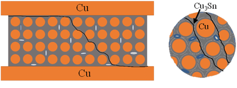 | ||
| Fig. 12 Schematic diagram of fracture path of the joints of Cu/Cu@Cu3Sn/Cu. | ||
Meanwhile, the joint fracture mode was investigated, corresponding fracture morphology and the specific phase distribution of shear samples reflowing at 280 °C for 40 min was analyzed. Fig. 13a and 13c was interface fracture and mixed fracture morphology, respectively. From the EDS results (Fig. 13b, and d)), it can be seen that marked points A, B, C in Fig. 13b) correspond to the phases of Cu3Sn, Cu and Cu3Sn, respectively, while the marked points A, B and C in Fig. 13d) correspond to the phases of Cu, Cu and Cu3Sn, respectively. This indicates that part of the cracks propagated along the inside of the Cu3Sn phase, the other part of the cracks extend along the Cu3Sn near the side of the Cu particle. In addition, the shear band morphology of Cu particles with ductile fracture can be observed in the fracture, and part of the Cu particles embedded in the IMCs undergo plastic deformation, indicating a ductile fracture mode at this time.
 | ||
| Fig. 13 Fracture morphology and EDS results of shear test sample after reflowing at 280 °C for 40 min with (a) and (b) interfacial fracture mode and (c) and (d) mixed fracture mode. | ||
Conclusions
(1) Electroplating Cu@Sn composite powder and its TLPS joint were prepared. The microstructure evolution discipline was illustrated during reflowing process. Special interfacial structure was designed due to the non-coplanar preform and DBC substrate, and compact interfacial interconnect come true in this study.(2) Growth kinetics of the Cu3Sn in Cu@Sn TLPS joint was investigated. The calculated active energy of Cu3Sn growth in Cu@Sn system is 50 kJ mol−1, which is smaller than that of Cu/Sn/Cu sandwich structure and traditional solder systems, because of the smaller content of low melting point phase and larger specific surface area and surface activity between Sn and Cu particles.
(3) The Cu/Cu3Sn joint shows excellent mechanical, thermal and electrical conductivity, the shear strength is no less than 48 MPa after aging at 400 °C for 1000 h, the thermal conductivity and electrical resistivity is 148 W m−1 K−1 and 5.1 μΩ cm, Young's modulus and hardness is 98.35 GPa and 2.62 Gpa, respectively. It is superior to the other Cu/Sn system in other investigations.
(4) The fracture behavior and failure mechanism of Cu@Cu3Sn joint was analyzed, the Z-shaped fracture path was found though both the interface and joint bulk, mixed fracture mode of the interface fracture of Cu/Cu3Sn and inside fracture of Cu3Sn phase was formed.
Author contributions
Conceptualization, Hongyan Xu; methodology, Hongyan Xu, Xuan Liu and Honghui Zhang; resources, Hongyan Xu, Ju Xu and Honghui Zhang; writing—original draft preparation, Honghui Zhang; writing—review and editing, Hongyan Xu and Honghui Zhang; supervision, Hongyan Xu; project administration, Hongyan Xu; funding acquisition, Hongyan Xu. All authors have read and agreed to the published version of the manuscript.Conflicts of interest
There are no conflicts to declare.Acknowledgements
This work was supported by Nature Science Foundation of Beijing under Grant No. 2222083.References
- https://www.gov.uk/government/uploads/system/uploads/attachment-data/file/31803/11-526-rohs-regulations-government-guidance-notes.pdf.
- A. Drevin-Bazin, F. Lacroix and J. F. Barbot, SiC Die Attach for High-Temperature Applications, J. Electron. Mater., 2014, 43, 695–701 CrossRef CAS.
- K. Chu, Y. Sohn and C. Moon, A comparative study of Cn/Sn/Cu and Ni/Sn/Ni solder joints for low temperature stable transient liquid phase bonding, Scr. Mater., 2015, 109, 113–117 CrossRef CAS.
- S. W. Yoon, M. D. Glover and K. Shiozaki, Nickel-Tin Transient Liquid Phase Bonding Toward High-Temperature Operational Power Electronics in Electrified Vehicles, IEEE Trans. Power Electron., 2013, 28(5), 2448–2456 Search PubMed.
- S. Park, et al., High-Temperature Die Attachment Using Sn-Plated Zn Solder for Power Electronics, IEEE Trans. Compon., Packag., Manuf. Technol., 2015, 5, 902–909 CAS.
- K. Chu, Y. Sohn and C. Moon, A comparative study of Cu/Sn/Cu and Ni/Sn/Ni solder joints for low temperature stable transient liquid phase bonding, Scri. Mater., 2015, 109, 113–117 CrossRef CAS.
- K. Guth, N. Oeschler, L. Bower, R. Speckels, G. Strotmann, N. Heuck, S. Krasel and A. Ciliox. New assembly and interconnect technologies for power modules. CIPS 2012, Germany Search PubMed.
- K. Guth, D. Siepe, J. Görlich, H. Torwesten, R. Roth, F. Hille and F. Umbach. New assembly and interconnects beyond sintering methods. New assembly and interconnects technology, PCIM Europe, 2010 Search PubMed.
- J. Watson and G. Castro, A review of high-temperature electronics technology and applications, J. Mater. Sci. Mater. Electron., 2015, 26, 9226–9235 CrossRef CAS.
- G. Zeng, S. McDonald and K. Nogita, Development of high-temperature solders, Rev. Mic. Rel., 2012, 52, 1306–1322 CAS.
- J. F. Li, P. A. Agyakwa and C. M. Johnson, Suitable Thicknesses of Base Metal and Interlayer, and Evolution of Phases for Ag/Sn/Ag Transient liquid-phase Joints Used for Power Die Attachment, J. Electron. Mater., 2014, 43, 983–995 CrossRef CAS.
- S. Shi, Preparation and Properties of High Temperature Lead-Free Cu-Sn Solder Paste, Doctoral Dissertation, Northeastern University, 2014 Search PubMed.
- H. Greve, L. Y. Chen, I. Fox and F. P. Mccluskey, Transient liquid phase sintered attach for power electronics, Electron. Compon. Technol. Conf., 2013, 435–440 CAS.
- H. Li, X. Liu, H. Y. Xu and J. Xu, Fabrication of joint based on Cu@Sn@Ag core–shell preform under ambient atmosphere for high-temperature applications, Weld World, 2022, 66, 1461–1470 CrossRef CAS.
- H. Y. Xu, J. Q. Li, P. Q. Ning and J. Xu, Microstructure evolution and properties evaluation of a novel bondline based on Cu@Sn Preform during temperature treatment, ICEPT, 2018, 1709–1715 Search PubMed.
- H. Y. Xu and J. Xu, Fabrication of highly reliable joint based on Cu/Ni/Sn double-layer powder for high temperature application, J. Microelectron. Electron. Packag., 2019, 16(4), 188–195 CrossRef.
- F. Kato, F. Lang, H. Nakagawa and et al., Thermal resistance evaluation of die-attachment made of nano-composite Cu/Sn TLPS paste in SiC power module[C], International Conference on Electronics Packaging (ICEP), 2017 Search PubMed.
- M. L. Li, L. Zhang and L. L. Gao, Interfacial structures and mechanical properties of Cu/Sn/Cu containing SiC nanowires under transient liquid phase bonding, Intermetallics., 2022, 148 CAS.
- T. Hu, H. Chen and M. Li, et al.) Microstructure evolution and thermostability of bondline based on Cu@Sn core-shell structured microparticles under high-temperature conditions, Mater. Des., 2017, 131, 196–203 CrossRef CAS.
- X. Liu, S. He and H. Nishikawa, Thermally stable Cu3Sn/Cu composite joint for high-temperature power device, Scr. Mater., 2016, 110, 101–104 CrossRef CAS.
- J. W. Yoon, S. Y. Bae and B. S. Lee, et al) Bonding of power device to ceramic substrate using Sn-coated Cu micro paste for high-temperature applications, Appl. Surf. Sci., 2020, 515, 146060 CrossRef CAS.
- J. Liu, K. Wang and F. Yu, A paste based on Cu@Sn@Ag particles for die attachment under ambient atmosphere in power device packaging, J. Mater. Sci. Mater., 2020, 3, 1808–1816 CrossRef.
- J.-W. Yoona, S. Baea, B.-S. Leea and S.-B. Jung, Bonding of power device to ceramic substrate using Sn-coated Cu micro paste for high-temperature applications, Appl. Surf. Sci., 2020, 515, 146060 CrossRef.
- Q. N. Zhu, M. Sheng and L. Luo, The effect of Pb contamination on the microstructure and mechanical properties of SnAg/Cu and SnSb/Cu solder joints in SMT, Solder. Surf. Mt. Technol., 2000, 12(3), 19–24 CrossRef CAS.
- S. T. Chua and K. S. Siow, Microstructural studies and bonding strength of pressureless sintered nano-silver joints on silver, direct bond copper (DBC) and copper substrates aged at 300 °C, J. Alloys Compd., 2016, 687(5), 486–498 CrossRef CAS.
- H. Greve, F. P. McCluskey and F. Patrick, Thermal Conductivity of Cu-Sn Transient Liquid Phase Sintered Interconnects for High Power Density Modules, IEEE, 2017 Search PubMed.
- X. W. Peng, Y. Ye, Z. Wang and J. H. Huang, Microstructural evolution and performance of high-tin-content Cu40Sn60 (wt. %) core/shell powder TLPS bonding joints, Journal of manufacturing processes, 2022, 75, 853–862 CrossRef.
- C. Titus, K. Girish and K. Narayan P, Effect of thermal contact heat transfer on solidification of Pb-Sn and Pb-free solders, Mater. Des., 2007, 28, 1006–1011 CrossRef.
- J. F. Yan, A Review of Sintering-Bonding Technology Using Ag Nanoparticles for Electronic Packaging, Nanomaterials, 2021, 11(4), 14 CrossRef PubMed.
| This journal is © The Royal Society of Chemistry 2022 |