
 Open Access Article
 This Open Access Article is licensed under a Creative Commons Attribution-Non Commercial 3.0 Unported Licence
Unveiling concentration effects on the structural and optoelectronic characteristics of Zn1−xCdxS (x = 0, 0.25, 0.50, 0.75, 1) cubic semiconductors: a theoretical study
Muhammad Aamir Iqbal *ab,
Maria Malikab,
Abu Zahidc,
Md. Rasidul Islamd,
Iván D. Arellano-Ramíreze and
Mohammed Al-Bahranif
*ab,
Maria Malikab,
Abu Zahidc,
Md. Rasidul Islamd,
Iván D. Arellano-Ramíreze and
Mohammed Al-Bahranif
aCentre of Excellence in Solid State Physics, University of the Punjab, Lahore 54590, Pakistan. E-mail: aamir.hum@gmail.com
bSchool of Materials Science and Engineering, Zhejiang University, Hangzhou 310027, China
cDepartment of Computer Science, Lamar University, Beaumont, Texas-77705, USA
dDepartment of Electrical and Electronic Engineering, Bangamata Sheikh Fojilatunnesa Mujib Science and Technology University, Melandah, Jamalpur-2012, Bangladesh
eDepartment of Physics, Universidad Tecnológica de Pereira, Pereira 660003, Colombia
fAir Conditioning and Refrigeration Techniques Engineering Department, Al-Mustaqbal University College, Babylon, 51001, Iraq
First published on 19th August 2022
Abstract
The structural and optoelectronic characteristics of Zn1−xCdxS (x = 0, 0.25, 0.50, 0.75, 1) semiconductors are reported using density functional theory within GGA, EV-GGA, and mBJ functionals. These semiconductors are observed in cubic symmetry at all Cd-concentrations and the lattice constant increases linearly with Cd-concentration while the bulk modulus shows a reverse behavior. These materials are direct bandgap semiconductors at all Cd-concentrations and their bandgap energy decreases from 3.67 eV to 2.59 eV. The isotropic optical properties of these direct bandgap semiconductors vary with Cd concentration as well, with absorption coefficients decreasing and absorbed near-UV light converting to visible blue light. Optical properties like refractive index, dielectric constant, conductivity, extinction coefficient, and reflectance are also displayed and discussed. These results provide useful theoretical understanding for the application of CdZnS semiconductors in photonic, photovoltaic, and optoelectronic devices.
1. Introduction
The usage of semiconductors has resulted in unprecedented advances in information processing, storage, and display applications, elevating the optoelectronics sector to the status of one of the most significant technical drivers of the economy.1 Semiconductor materials of groups II–VI are very significant, and their characteristics may be tailored for distinct applications by changing the composition of the component elements for use in well-known commercial optoelectronic devices functioning throughout broad spectrum ranges. The direct bandgap of II–VI semiconductors of Cd substituted ZnS alloys makes them very appealing for numerous device applications in the photonic, photovoltaic, and optoelectronic industry spectral regions.1–4 These semiconductors can also be employed in the fabrication of detectors and in infrared focal plane arrays.5,6The Zn1−xCdxS (x = 0, 0.25, 0.50, 0.75, and 1) semiconductors have been studied theoretically and synthesized experimentally by many researchers.7–15 The alloy films of CdxZn1−xS were prepared using the evaporation method to investigate the structural properties as a function of substrate temperature,7 whereas Yamada et al. studied optical gain formation in CdxZn1−xS strained layer quantum wells.8 Valkonen et al. deposited thin films of CdxZn1−xS by using the SILAR method,9 while Raviprakash et al. deposited thin films of CdxZn1−xS (x = 0, 0.2, 0.4, 0.6, 0.8, 1) employing the chemical spray pyrolysis technique at a temperature of 573 K for photovoltaic applications,10 and their XRD results reveal hexagonal structure for all deposited crystalline films. Kumar et al. studied the structural, and optical characteristics of CdZnS thin films with absorption spectra in the wavelength range of 400–650 nm.11 Korozlu et al. studied physical properties such as structural, electronic, and optical characteristics of CdxZn1−xS compounds using the pseudo-potential method within the CASTEP code.12 Ramasamy et al. synthesized transition metal (Cd) doped ZnS alloys using the chemical precipitation method, and their XRD results reveal a cubic structure having a mean size in the range of 4–6 nm.13 Noor et al. also investigated physical characteristics including electronic, structural, and optical properties of CdxZn1−xS alloys within LDA and GGA (WC) functional.14 Iranmanesh et al. synthesized CdxZn1−xS (x = 0, 0.2, 0.4, 0.6, 0.8, 1) nanoparticles employing the co-precipitation method under ultrasonic irradiation, and their prepared nanoparticles were all in cubic symmetry in the range of 3–4 nm.15
The structural and optoelectronic characteristics of Cd-substituted ZnS alloys are significant in defining features such as inter-atomic forces, electron–photon interactions, and transport coefficients.1,14 This work is aimed at enhancing existing data compared with cited work on the electronic properties and adding optical parameters using an all-electron approach. We investigated the structural and optoelectronic characteristics of CdxZn1−xS (x = 0, 0.25, 0.50, 0.75, 1) compounds using DFT within GGA, EV-GGA, and mBJ functionals, and then compared them to available experimental15 and theoretical data12,14 to provide a clear and additional understanding for their use in electronic, photonic, photovoltaic, and optoelectronic devices with a cubic symmetry. This work is innovative and reports cubic crystal symmetry at all Cd-concentrations, specifically at x = 0.50, and provides a possible future direction for synthesizing CdZnS alloys having a cubic symmetry with manipulation of doping components for numerous device-based applications in the domain of photonics, photovoltaics, and optoelectronics.
2. Theoretical method
The full-potential linearized augmented plane-wave (FP-LAPW) method is employed to solve the Kohn–Sham equations16 using the Wien2k code17 within the framework of density functional theory (DFT),18 in which the FP-LAPW method treats muffin-tin spheres and interstitial regions to determine eigen values to estimate physical properties. Basis functions are characterized by the Fourier series, whereas an analytical solution of the Schrodinger wave equation is employed to represent the spherical component of the potential multiplied by spherical harmonics. The charge and potential are signified by inside muffin-tin spherical harmonics up to Lmax = 10. The Rmt × Kmax is set to be 7 while the Gmax used is 12. The muffin-tin radii used for structure generation are 2.30, 2.34, 2.40, 2.44 for Zn, 2.34, 2.40, 2.44, 2.48 for Cd, and 1.88, 1.92, 1.96, 2.00, 2.03 for S. The energy of 10−6 Ry separates the core and valence states, whereas the total energy was calculated using a set of 56 k-points in the irreducible set of the Brillion zone (IBZ), comparable to the Monkhorst Pack19 grid of 12 × 12 × 12. The SCF calculations are converged as the total energy and charge of the system are stable within 0.00001 Ry and 0.0001 e, respectively. The generalized gradient approximation (PBE)20 has been used as an exchange-correlation functional for structural optimization, while electronic band structures are computed within the generalized gradient approximation of Engel and Vosko (EV-GGA),21 GGA, and the modified Becke–Jhonson method (mBJ) proposed by Tran and Blaha.22 The tuned optical spectra are explored within the mBJ approximation only, which yields results very comparable to experiments.3. Results and discussion
3.1 Structural and electronic characteristics
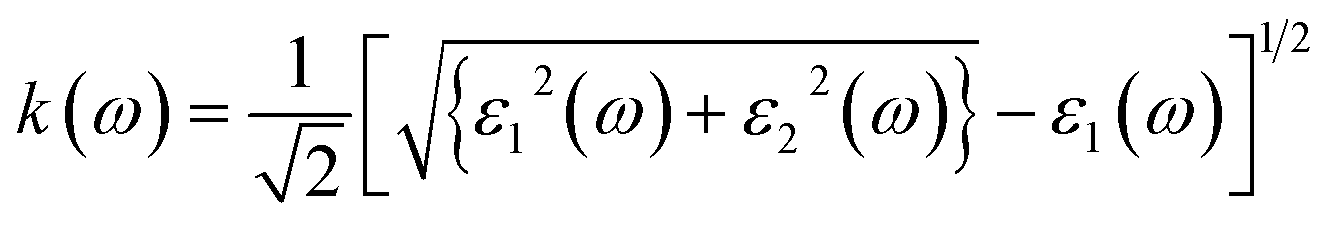
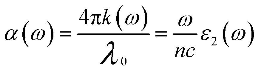
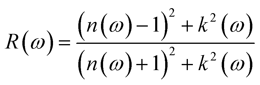
The optimized lattice parameter at equilibrium can be obtained at a minimum energy correlating to ground state volume, which can be further used to explore all of the physical properties of a crystal. The equilibrium lattice parameters were computed using Murnaghan's equation of states (EOS),23 and the optimization plots are portrayed in Fig. 1. Variation in structural parameters with Cd-concentration is depicted in Fig. 2. A unit cell of CdZnS has been generated to investigate the Cd-compositional factor to explore the structural properties of Cd-substituted ZnS semiconductors, and a cubic crystal symmetry is observed at all Cd-concentrations. The crystal structure of CdZnS at a Cd-concentration of x = 0.50 is shown in Fig. 2a. The approximated lattice constant, bulk modulus, and electronic bandgap for each Cd-composition along with other experimental and theoretical data is summarized in Table 1. It is established that the lattice constant varies linearly with an increase in Cd-concentration as shown in Fig. 2b and nearly follows Vegard's law,24 which narrates that the lattice constant of a crystal structure of an alloy and the concentration of the component elements at constant temperature have a linear relationship. Both the linear increase in lattice constant and the abrupt volume increase could be explained by the increased mass of Cd atoms substituted on Zn cites with compositional factor ‘x’. Fig. 2c depicts variation in bulk modulus, while Fig. 2d portrays volume variation with Cd-concentration. | ||
| Fig. 1 Ground state volume vs. energy plots with Cd-concentrations (0, 0.25, 0.50, 0.75, 1). | ||
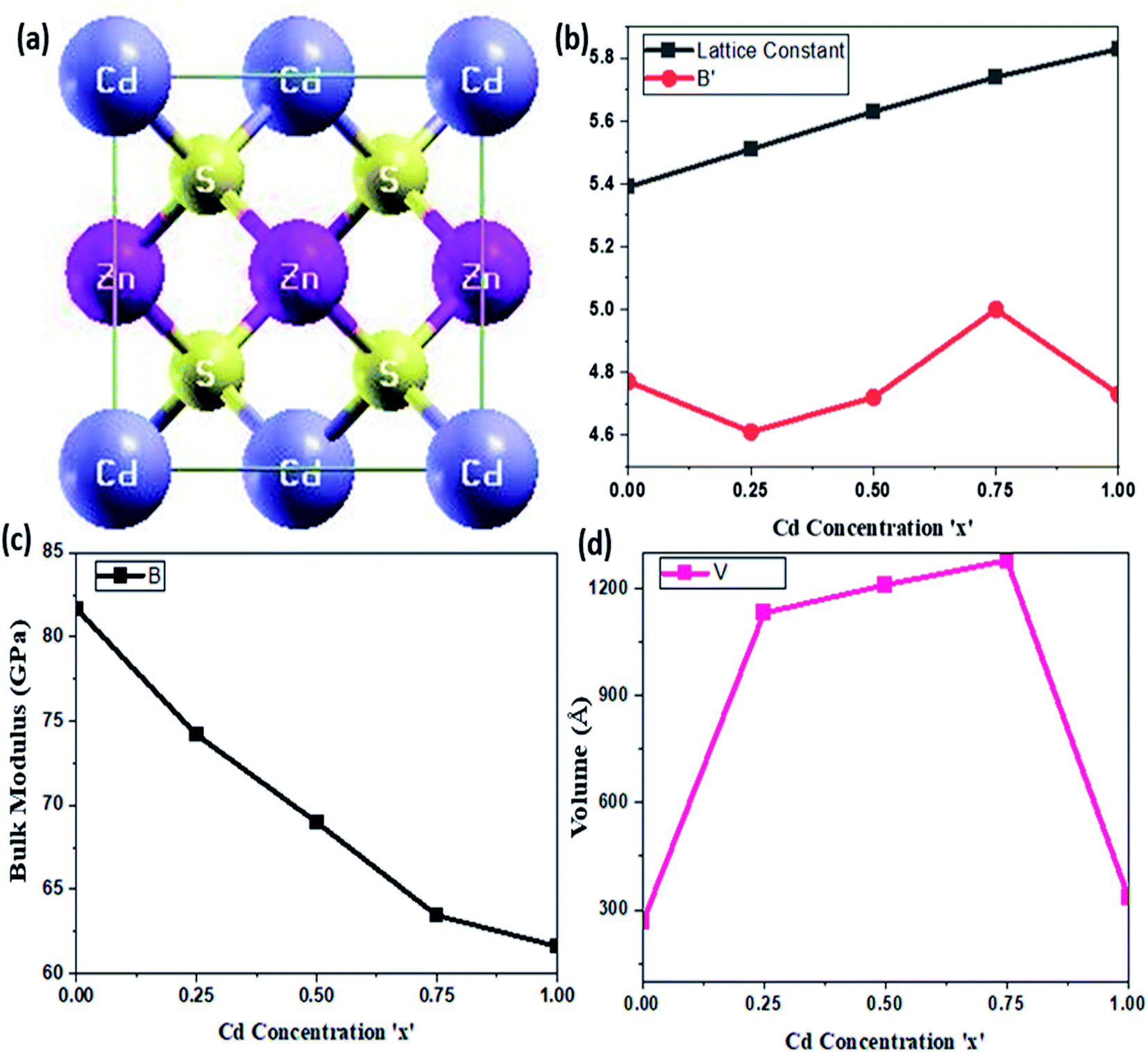 | ||
| Fig. 2 Concentration dependent parameters, (a) crystal structure of Cd0.50Zn0.50S alloy depicting cubic symmetry, (b) variation in lattice constant and derivative of bulk modulus, (c) variation of bulk modulus, and (d) volume variation with Cd-concentration. | ||
| Semiconductor | Lattice constant (Å) | Bulk modulus (GPa) | ||||
|---|---|---|---|---|---|---|
| Present work | Experimental | Theoretical | Present work | Experimental | Theoretical | |
| ZnS | 5.39 | 5.41 (ref. 25) | 5.36 (ref. 14) | 81.67 | 76.90 (ref. 25) | 73.97 (ref. 14) |
| 5.31 (ref. 14) | 87.13 (ref. 14) | |||||
| 5.43 (ref. 12) | 80.66 (ref. 12) | |||||
| Cd0.25Zn0.75S | 5.51 | — | 5.44 (ref. 14) | 74.19 | — | 79.98 (ref. 14) |
| 5.50 (ref. 14) | 72.21 (ref. 14) | |||||
| 5.53 (ref. 12) | 76.41 (ref. 12) | |||||
| Cd0.50Zn0.50S | 5.63 | — | 3.90 (ref. 14) | 68.99 | — | 74.01 (ref. 14) |
| 3.98 (ref. 14) | 67.88 (ref. 14) | |||||
| 3.96 (ref. 12) | 71.87 (ref. 12) | |||||
| Cd0.75Zn0.25S | 5.74 | — | 5.66 (ref. 14) | 63.46 | — | 70.65 (ref. 14) |
| 5.74 (ref. 14) | 62.91 (ref. 14) | |||||
| 5.73 (ref. 12) | 68.94 (ref. 12) | |||||
| CdS | 5.83 | 5.82 (ref. 25) | 5.76 (ref. 14) | 61.63 | 62.00 (ref. 25) | 67.40 (ref. 14) |
| 5.83 (ref. 12 and 14) | 61.37 (ref. 14) | |||||
| 65.94 (ref. 12) | ||||||
The calculated lattice parameters, as mentioned in Table 1, are compared with the available experimental and theoretical results, and show a cubic structure at a Cd-concentration of x = 0.50, which is a significant improvement over other theoretical results and agrees well with the available literature.15 The bulk modulus of Cd-substituted ZnS semiconductors decreases as the Cd-component rises, implying that the hardness of these materials reduces, indicating a ductile character. As ZnS has a larger bulk modulus than Cd-based ZnS alloys, its compressibility is lower than that of CdS semiconductor.
The density of states (DOS) and electronic band structures of Cd-substituted ZnS alloys along the direction of high symmetry points in the first Brillouin zone are investigated, and their direct bandgap nature is shown to drop almost linearly with increasing Cd-component (Fig. 3). Fig. 3a portrays the density of states for the Cd-component at x = 0.50, estimated within mBJ potential by taking fermi energy at 0 eV, while the band-structures for all Cd-concentrations in the energy range of −8 to 8 eV are displayed in Fig. 4. Table 2 summarizes the bandgap energy values, and Fig. 3b shows a zoom of the partial density of states depicting variation trends in Cd, Zn, and S atoms p and d states with an increase in Cd-substitution. The predicted bandgap energies computed within the mBJ functional are in agreement with the experimentally reported results,26 proving it as the best approximation to depict the electronic structures of these semiconductors, while band energies are underestimated in EV-GGA and GGA results. The mBJ shifts the conduction band more in comparison to GGA and EV-GGA, and yields improved results. Bandgap energies computed within mBJ with Cd-component (0, 0.25, 0.50, 0.75, 1) in comparison with EV-GGA, Korozlu,12 and Noor14 results are shown in Fig. 3c. Also, both the valence and conduction band maxima and minima are positioned in the identical k-space region, indicating that these compounds have direct bandgap energies ranging from 3.67 to 2.59 eV, depicting characteristics of a semiconductor at all Cd-concentrations.
 | ||
| Fig. 3 (a) total and partial density of states of Cd0.50Zn0.50S alloy, (b) a zoom of partial density of states depicting variation in Cd, Zn, and S atom p, d states, (c) bandgap variation with Cd-concentration, and (d) variation in ε1(0)with Cd-concentration. | ||
 | ||
| Fig. 4 Band structures computed within mBJ at varying Cd-concentrations (0, 0.25, 0.50, 0.75, 1). | ||
| Semiconductor | Bandgap (eV) | Static dielectric constant | ||||
|---|---|---|---|---|---|---|
| Present work | Experimental | Theoretical | Present work | Experimental | Theoretical | |
| ZnS | 3.67 | 3.73 (ref. 26) | 2.00 (ref. 14) | 4.57 | 5.20 (ref. 27) | 6.38 (ref. 14) |
| 1.74 (ref. 12) | 5.50 (ref. 12) | |||||
| 4.59 (ref. 28) | ||||||
| Cd0.25Zn0.75S | 3.28 | — | 1.60 (ref. 14) | 4.52 | — | 6.44 (ref. 14) |
| 1.53 (ref. 12) | 5.42 (ref. 12) | |||||
| 2.61 (ref. 30) | ||||||
| 3.34 (ref. 30) | ||||||
| Cd0.50Zn0.50S | 3.01 | — | 1.20 (ref. 14) | 4.47 | — | 6.53 (ref. 14) |
| 1.43 (ref. 12) | 5.56 (ref. 12) | |||||
| Cd0.75Zn0.25S | 2.81 | — | 1.00 (ref. 14) | 4.41 | — | 6.58 (ref. 14) |
| 1.38 (ref. 12) | 5.10 (ref. 12) | |||||
| CdS | 2.59 | 2.55 (ref. 25) | 0.90 (ref. 14) | 4.33 | 6.61 (ref. 14) | |
| 2.44 (ref. 29) | 1.26 (ref. 12) | 4.87 (ref. 12) | ||||
To provide a clear explanation of the computed band structures and orbital origins, total and partial density of states are also computed. The total and partial DOS of Cd substituted ZnS semiconductors are similar with a difference in peak height and energy, so only DOS at the Cd-component at x = 0.50 is shown in Fig. 3a and b. As the results obtained for band structures within mBJ are well aligned to experiments, the density of states is portrayed and discussed within mBJ only wherein it corresponds to three regions in the valence band, the first of which is mainly made of hybridization of S-d and Cd-p states, with a small amount of S-p and Zn-d states. The valence band peak occurs in the region from −5.12 eV to −5.71 eV, which is mainly made of Zn-d states in addition to Cd-p and S-p, S-d states. The third region, −6.89 eV to −5.71 eV, is mainly composed of Cd-s states with the addition of S-p, S-d, and Zn-d states. The conduction band is mainly made of Zn-d and S-p, S-d states with the addition of a small amount of Cd-p, Cd-d states, whereas hybridization of Cd, Zn, and S atoms depicts the covalent bond nature of these alloys.
3.2 Optical properties
In photonics and optoelectronics, the interaction of light with matter is extremely important. When light interacts with semiconductors, the frequency of incoming photon energy is the most important factor in determining the reaction of matter, resulting in optical phenomena. Excitation spectra are produced when an incident photon interacts with a material's surface, changing the electrons probability transitioning from a filled to an unfilled state. The subsequent excitation spectrum can be described by joint densities, and the linear response of the understudied system may be explained by a complex dielectric function,31 which can be represented as;| ε(ω) = ε1(ω) + iε2(ω) | (1) |
 | (2) |
 | (3) |
Optical constants like refractive index and coefficient of extinction may be inferred from incoming radiation-dependent dielectric functions. The index of refraction, n(ω) delivers statistics concerning the drop in speed of incoming radiation when it passes through a medium and is subjected to the frequency of the incoming radiation.33 The n(ω) and k(ω) can be approximated as follows:
 | (4) |
 | (5) |
The absorption coefficient33 can be used to describe the optical absorption of a medium, and it is calculated using the imaginary component of the index of refraction. The absorption coefficient can be used to investigate how the intensity of radiation in a material decay with distance, and can be written as:
 | (6) |
Reflection spectrum study explores the behavior of the surface of the materials when light falls on the surface,33 and can be approximated as follows:
 | (7) |
The optical conductivity33 is the extension of electrical transport to high optical frequencies which is a contact free quantitative measurement; mostly sensitive to charged responses, and may be deduced from ε2(ω). The k(ω) closely tracks ε2(ω), whereas optical conductance may be ascribed by variation of k(ω) with ε2(ω) as:
 | (8) |
The electron energy loss function of the interacting electrons33 can be mathematically defined as:
 | (9) |
The Cd-substituted ZnS alloys have cubic symmetry, so their optical response is isotropic. A denser mesh of k points is used to study optical properties up to 30 eV of incoming radiation within mBJ functional. Fig. 5 and 6 depicts all the optical parameters and the dependency of static ε1(ω = 0 Hz) on semiconductor bandgap can be narrated using the Penn model,34 which may be written as:
 | (10) |
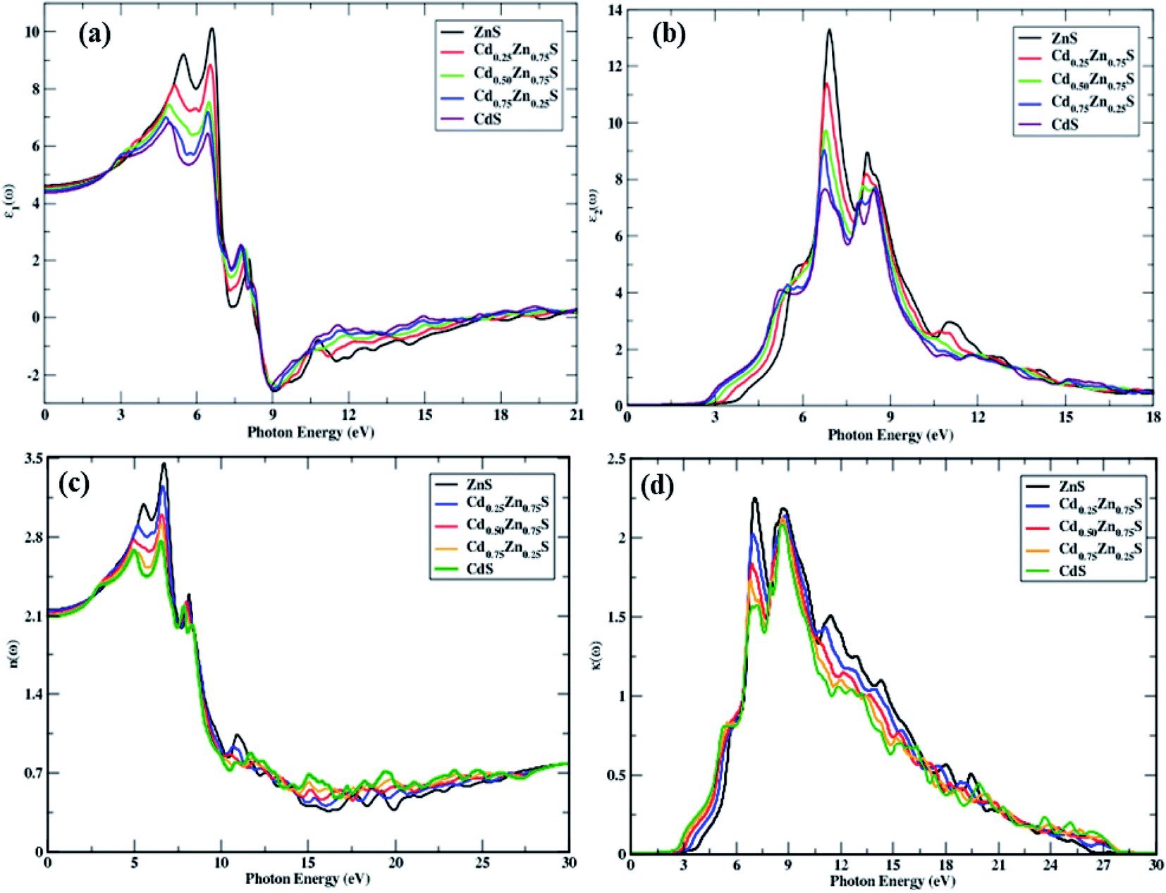 | ||
| Fig. 5 Complex dielectric function and optical parameters, (a) ε1(ω), (b) ε2(ω), (c) n(ω), and (d) k(ω) variation with Cd-component (0, 0.25, 0.50, 0.75, 1). | ||
 | ||
| Fig. 6 Optical parameters under the effect of compositional factor ‘x’, (a) absorption, (b) optical conductance, (c) reflectance, and (d) energy loss function with Cd-component (0, 0.25, 0.50, 0.75, 1). | ||
A trend of rapid increase, minor decline, and then again, a rise to the highest peak values for the real portion of the dielectric function can be observed in Fig. 5a. It is also apparent that ε1(ω) has more transitions in the energy range of 2.85–6.95 eV while the height of the peak decreases and moves to lower values with a rise in Cd-concentration. Because all incoming photons in the energy region of 8.3–18.6 eV are reflected, a metallic nature is visible below zero-unit values. As a result, these materials can be employed to shield the vacuum and extreme UV radiation. After 20 eV, the negative spectra becomes positive and stable, indicating that these alloys do not interact with high energy radiation and may thus be utilized for optical lenses. The static dielectric constant decreases with an increase in the Cd-component, and the obtained values are summarized in Table 2, along with their decreasing trend, which is portrayed in Fig. 3d.
The threshold energies of ε2(ω) are found to decrease with the Cd-component, and these points depict direct interband transitions from the uppermost valence band to the lowermost conduction band, whereas beyond these points, there is a quick increase in the imaginary portion of dielectric function spectra against incident radiation, up to 6.97 eV. In the energy range between the absorption threshold and 27 eV of incoming radiation, there are four main peaks that can be seen in this range, as depicted in Fig. 5b. The highest threshold value is observed for ZnS, and it decreases with the Cd-component. The peak height decreased from 13.22 to 7.58 units, and the Cd-component shifted their spectra to lower energies. A constant spectrum above 20 eV is seen that vanishes at 27.44 eV of incident photon energy. Hence, these materials have an ignorable absorption coefficient at energies of 27.44 eV and higher.
Optical absorptance is depicted in Fig. 6a, which is primarily attributed by ε2(ω) and larger absorption values correlate to larger values of the imaginary component of the dielectric function. Under study materials show an absorption decrease from 194.53 to 183.33 units with a Cd-component, while the extreme peak corresponds to ZnS. CdS has a high α(ω) above 19.9 eV of incoming photons in comparison to all other materials. Above 27.92 eV of entering photon energy, a steady trend is seen, whereas photons with energies much less than the bandgap energy show no absorption. These materials have high absorption in the energy region of 6.41–27.92 eV and new-fangled peaks in this section arise from electronic transitions from the valence band to the conduction band. Peak shifts towards lesser energies are also observed, with a blue shift with a Cd-component.
Solids have frequency-dependent optical characteristics, and because all CdZnS semiconductors are in cubic symmetry, the index of refraction is identical in both transverse directions. Fig. 5c portrays the static refractive index, which decreases with the Cd-component and novel peaks in the energy range of 6.46–25 eV are detected. The n(0) varies with the Cd-component, ranging from 3.48 to 2.74 units, and the steady response of these materials may be observed in the spectrum at 28 eV of entering radiation. Fig. 5d illustrates the quick rise in threshold energies and the decrease in maximum peak height with the Cd-component. The main peaks range from 2.26 to 1.57 with a Cd-component of x = 0, 0.25, 0.50, 0.75, 1. There is no spectrum seen above 27.50 eV of incoming photons as these materials do not relate to radiation having a higher energy of 27.50 eV, depicting ignorable absorption. A decreasing trend is observed in n(ω), and k(ω) with the Cd-component.
As σ(ω) can be shown in Fig. 6b, the optical conductivity is minimum (zero) as long as the arriving photons have less energy than the bandgap energy; however, as Cd-concentration increases, the peak height reduces from 11.09 to 6.24 values. In the energy range of 5–12.5 eV, there are more peaks, and a steady response may be seen at 27.80 eV of incoming light. CdS has high optical conductance in the 19.50–26.90 eV energy range, and these materials show a high conductance value in the region of 5–12.5 eV of incident radiation, indicating that they are optically active in this part.
A rapid increase can be seen in the reflectance spectrum with an increase in incoming photon energy as shown in Fig. 6c. A peak shift towards lower energy values is also observed in conjunction with a broader spectrum, while the height of the peak decreases with Cd-component with disseminative humps, which are seen in the incoming energy range of 5–25 eV. The maximum reflectance value corresponds to ZnS, and it decreases as Cd substitutes Zn atoms. The R(0) values are observed to decrease from 0.133 to 0.124 units as the Cd-component increases, and new peaks are also witnessed in the incoming energy range of 5–20 eV.
When the energy of the entering light is less than the bandgap energy, no electron energy loss occurs. As a result, there is no scattering of electrons below the bandgap energy, while inelastic scattering of electrons happens above the bandgap energy, resulting in a spectrum which is proportionate to the received light. It may be seen from Fig. 6d that the high value of the electron energy loss function links to ZnS at an entering energy of 20.09 eV and it decreases with the Cd-component. The loss function of interacting electrons is found to be negligible under 5 eV and significant above 27 eV of entering photons, with main peaks detected in the 10.29–28 eV energy range. As the concentration of Cd rises, the peak height appears to be shifting towards lower values.
4. Conclusions
This research explored structural and optoelectronic properties of Cd-substituted ZnS semiconductors using the FP-LAPW method within DFT, in which all of these compounds are found to exhibit a cubic symmetry, with the lattice constant increasing linearly and the bulk modulus decreasing with Cd-component. The predicted band structures and density of states imply that these materials have semiconductor characteristics, whereas the bandgap decreases with the Cd-component. These Zn1−xCdxS (x = 0, 0.25, 0.50, 0.75, 1) semiconductors have cubic symmetry for all Cd-concentrations, resulting in an isotropic optical response. The optical spectrum is observed in the range of visible blue to near-ultra violet radiation, and these alloys are found to be optically active in the 5–12.5 eV range of incident radiation, with potential applications as optical detectors and optical lenses in the photonic, photovoltaic, and optoelectronic industries.Author contributions
Conceptualization, M. A. I.; methodology, M. A. I.; formal analysis, M. A. I.; writing—original draft preparation, M. A. I.; software, M. A. I.; writing—review and editing, M. A. I., M. M., A. Z., M. R. I., and I. D. A. R.; project administration, M. A. I. All authors have read and agreed to the published version of the manuscript.Conflicts of interest
The authors declare no conflict of interests.References
- S. Colak, in II-VI Semiconductor Compounds, World Scientific, 1993, pp. 397–426 Search PubMed.
- M. C. Tamargo, II-VI semiconductor materials and their applications, CRC Press, 2002, vol. 12 Search PubMed.
- S. M. Mosavi and H. Kafashan, Superlattices Microstruct., 2019, 126, 139–149 CrossRef CAS.
- M. A. Iqbal, M. Malik, W. Shahid, S. Irfan, A. C. Alguno, K. Morsy, R. Y. Capangpangan, P. V. Pham and J. R. Choi, Sci. Rep., 2022, 12, 1–12 CrossRef PubMed.
- L. Hannachi and N. Bouarissa, Superlattices Microstruct., 2008, 44, 794–801 CrossRef CAS.
- M. A. Iqbal, M. Malik, W. Shahid, S. Z. U. Din, N. Anwar, M. Ikram and F. Idrees, Thin Films Photovoltaics, 2022, 5 Search PubMed.
- V. D. Vankar, S. R. Das, P. Nath and K. L. Chopra, Phys. Status Solidi A, 1978, 45, 665–669 CrossRef CAS.
- Y. Yamada, Y. Masumoto and T. Taguchi, Phys. B, 1993, 191, 83–89 CrossRef CAS.
- M. P. Valkonen, S. Lindroos and M. Leskelä, Appl. Surf. Sci., 1998, 134, 283–291 CrossRef CAS.
- Y. Raviprakash, K. V Bangera and G. K. Shivakumar, Sol. Energy, 2009, 83, 1645–1651 CrossRef CAS.
- P. Kumar, A. Misra, D. Kumar, N. Dhama, T. P. Sharma and P. N. Dixit, Opt. Mater., 2004, 27, 261–264 CrossRef CAS.
- N. Korozlu, K. Colakoglu and E. Deligoz, Phys. Status Solidi B, 2010, 247, 1214–1219 CrossRef CAS.
- V. Ramasamy, K. Praba and G. Murugadoss, Spectrochim. Acta, Part A, 2012, 96, 963–971 CrossRef CAS.
- N. A. Noor, N. Ikram, S. Ali, S. Nazir, S. M. Alay-e-Abbas and A. Shaukat, J. Alloys Compd., 2010, 507, 356–363 CrossRef CAS.
- P. Iranmanesh, S. Saeednia and N. Khorasanipoor, Mater. Sci. Semicond. Process., 2017, 68, 193–198 CrossRef CAS.
- W. Kohn and L. J. Sham, Phys. Rev., 1965, 140, A1133 CrossRef.
- P. Blaha, K. Schwarz, G. K. H. Madsen, D. Kvasnicka and J. Luitz, An augmented plane wave + local orbitals program for calculating crystal properties, 2001 Search PubMed.
- M. A. Iqbal, N. Ashraf, W. Shahid, D. Afzal, F. Idrees and R. Ahmad, Density Functional Theory-Recent Advances, New Perspectives and Applications, 2021 Search PubMed.
- H. J. Monkhorst and J. D. Pack, Phys. Rev. B: Solid State, 1976, 13, 5188 CrossRef.
- S. De Waele, K. Lejaeghere, M. Sluydts and S. Cottenier, Phys. Rev. B: Condens. Matter Mater. Phys., 2016, 94, 235418 CrossRef.
- E. Engel and S. H. Vosko, Phys. Rev. B: Condens. Matter Mater. Phys., 1993, 47, 13164 CrossRef CAS.
- D. J. Singh, Phys. Rev. B: Condens. Matter Mater. Phys., 2010, 82, 205102 CrossRef.
- V. G. Tyuterev and N. Vast, Comput. Mater. Sci., 2006, 38, 350–353 CrossRef CAS.
- L. Vegard, J. Phys., 1921, 5, 393–395 CAS.
- O. Zakharov, A. Rubio, X. Blase, M. L. Cohen and S. G. Louie, Phys. Rev. B: Condens. Matter Mater. Phys., 1994, 50, 10780 CrossRef CAS PubMed.
- S. Nazir, N. Ikram, S. A. Siddiqi, Y. Saeed, A. Shaukat and A. H. Reshak, Curr. Opin. Solid State Mater. Sci., 2010, 14, 1–6 CrossRef CAS.
- F. Kootstra, P. L. De Boeij and J. G. Snijders, Phys. Rev. B: Condens. Matter Mater. Phys., 2000, 62, 7071 CrossRef CAS.
- M. Bilal, M. Shafiq, I. Ahmad and I. Khan, J. Semicond., 2014, 35, 72001 CrossRef CAS.
- P. Kumar, A. Misra, D. Kumar, N. Dhama, T. P. Sharma and P. N. Dixit, Opt. Mater., 2004, 27, 261–264 CrossRef CAS.
- M. A. Iqbal, A. Ahmad, M. Malik, J. R. Choi and P. V Pham, Materials, 2022, 15, 2617 CrossRef CAS.
- L. Novotny and C. Hafner, Phys. Rev. E: Stat. Phys., Plasmas, Fluids, Relat. Interdiscip. Top., 1994, 50, 4094 CrossRef CAS PubMed.
- D. W. Johnson, J. Phys. A: Math. Gen., 1975, 8, 490 CrossRef.
- M. Fox, Optical Properties of Solids, 2002 Search PubMed.
- D. R. Penn, Phys. Rev., 1962, 128, 2093 CrossRef CAS.
| This journal is © The Royal Society of Chemistry 2022 |