
 Open Access Article
 This Open Access Article is licensed under a Creative Commons Attribution-Non Commercial 3.0 Unported Licence
Critical current density improvement in CSD-grown high-entropy REBa2Cu3O7−δ films
Pablo Cayado†
 *ab,
Lukas Grünewald†*c,
Manuela Erbea,
Jens Hänisch*a,
Dagmar Gerthsenc and
Bernhard Holzapfela
*ab,
Lukas Grünewald†*c,
Manuela Erbea,
Jens Hänisch*a,
Dagmar Gerthsenc and
Bernhard Holzapfela
aKarlsruhe Institute of Technology (KIT), Institute for Technical Physics (ITEP), Hermann-von-Helmholtz-Platz 1, 76344 Eggenstein-Leopoldshafen, Germany. E-mail: pablo.cayado@unige.ch; jens.haenisch@kit.edu
bUniversity of Geneva, Department of Quantum Matter Physics (DQMP), Quai Ernest-Ansermet 24, 1211 Geneva, Switzerland
cKarlsruhe Institute of Technology (KIT), Laboratory for Electron Microscopy (LEM), Engesserstr. 7, 76131 Karlsruhe, Germany. E-mail: lukas.gruenewald@kit.edu
First published on 11th October 2022
Abstract
High-entropy oxide (HEO) superconductors have been developed since very recently. Different superconductors can be produced in the form of a high-entropy compound, including REBa2Cu3O7−δ (REBCO). However, until now, mainly bulk samples (mostly in polycrystalline form) have been reported. In this work, the first CSD-grown high-entropy (HE) REBCO nanocomposite films were successfully synthesized. In particular, high-quality Gd0.2Dy0.2Y0.2Ho0.2Er0.2Ba2Cu3O7−δ nanocomposite films with 12 mol% BaHfO3 nanoparticles were grown on SrTiO3 substrates. The X-ray diffraction patterns show a near-perfect c-axis oriented grain growth. Both Tc and 77 K Jsfc, 91.9 K and 3.5 MA cm−2, respectively, are comparable with the values of the single-RE REBCO films. Moreover, at low temperatures, specifically at 30 K, the Jc values are larger than those of the single-RE samples. A transmission electron microscopy (TEM) study, including energy-dispersive X-ray spectroscopy (EDXS) measurements, reveals that the different RE3+ ions are distributed homogeneously in the matrix without forming clusters. This distribution causes point-like pinning centres that explain the superior performances of these samples at low temperatures. Although still seen as a proof-of-concept for the feasibility of preparing such films, these results demonstrate that the HE REBCO films are a promising option for the future fabrication of high-performance coated conductors. In the investigated B–T range, however, their Jc values are still lower than those of other, medium-entropy REBCO films, which shows that an optimization of the composition of the HE REBCO films is needed to maximize their performance.
1. Introduction
In recent years, REBa2Cu3O7−δ (REBCO) compounds have been a subject of intense research due to their use as base materials for Coated Conductors (CCs). Their remarkably high critical temperature (Tc) and high critical current density (Jc) in a large range of temperatures and magnetic fields predestined them as the most suitable compounds for the preparation of CCs. These notable properties of the CCs imply that they can be employed in various applications such as fault current limiters (FCLs), generators, or high-field magnets.1–3In general, the use of these compounds in commercial CC fabrication by different companies is restricted to a few of them with YBa2Cu3O7−δ (YBCO) and GdBa2Cu3O7−δ (GdBCO) being by far the most commonly used.4,5 This limited number is mainly explained by difficulties in synthesizing other REBCO compounds due to the ill-fitting of the RE ions in the crystal structure, which increases the instability of the compound significantly.6–9 On the one hand, larger RE ions, like Sm3+ or Nd3+, have a certain tendency to substitute the Ba2+ ions and, on the other hand, smaller RE ions, such as Lu3+ or Yb3+, lead to strong and detrimental lattice distortions and a larger defect density through vacancies on the RE site.10 This complicates the synthesis of these other REBCO compounds since both factors contribute to decreasing phase stability. However, once successfully synthesized, these alternative REBCO compounds could offer excellent properties even superior to YBCO.6,11–13
Considering these difficulties, a new strategy based on mixing several REBCO compounds started to play an important role. It was developed to benefit from improved properties of alternative REBCO compounds but, at the same time, reduce the complexity of the synthesis. By mixing REBCO, their individual synthesis windows (especially in deposition temperature Tdep and oxygen partial pressure pO2) can be merged, and hence the available final synthesis window enlarged. The approach of mixing REBCO combining two or three compounds was employed multiple times in the past.10,14–20 The improvement in the superconducting properties reported for these mixed compounds is mainly related to the distribution of the different RE3+ ions in the matrix creating strained regions in localized areas and concomitant Tc fluctuations.14,21,22
In the last five years, another step forward in the mixing strategy was taken with the appearance of the so-called High-Entropy Alloy (HEA) superconductors (for a review, see e.g. Sun and Cava23 and Kitagawa et al.24). A HEA is generally defined as an alloy made of five or more constituent elements with a concentration range between 5 and 35 at%. This concept of high entropy has been generalized to other material classes, such as intermetallics and ceramics,25 especially oxides.26 In these high-entropy oxides (HEO), the elemental mixing is restricted to one or some of the atomic positions.
The first HEA-type superconductor was discovered in the Ti–Zr–Hf–Nb–Ta system.27 Later, the concept of mixing multiple compounds inside the same matrix was extended to other types of superconductors like BiS2-based,28 van-der-Waals,29 rock-salt-type,30,31 A15-type32 and transition-metal-zirconide (TrZr2)-type superconductors,33 and hence extended to intermetallics and compounds with non-metallic constituents. Only in the last couple of years was this approach also applied to the oxide REBCO compounds.34–36 However, all these early studies on “HEO-type” REBCO compounds (HE REBCO) were undertaken on bulk samples, and only recently a work about HE REBCO films prepared by Pulsed Laser Deposition (PLD) was published.37 Interestingly, superconductivity has not been found in high-entropy Ruddlesden–Popper-type cuprates, the so-called 214 phases so far.38
In this work, we used chemical solution deposition (CSD), particularly the well-known TFA-MOD route,39 to prepare HE REBCO nanocomposite films by CSD for the first time. We included BaHfO3 (BHO) nanoparticles following the so-called “in situ” approach.12,40 As references served a single-RE (Gd) film and two “medium-entropy oxides” (MEO) films with two (2MEO, Y0.5Gd0.5Ba2Cu3O7−δ) and three (3MEO, Y0.33Er0.33Ho0.33Ba2Cu3O7−δ) RE elements. MEO may refer to mixtures of 2–4 components.
The results show that the preparation of this type of films by CSD with excellent quality is possible and demonstrate their potential at low temperatures.
2. Results and discussion
2.1. Optimisation of the growth
One of the main challenges when using CSD to prepare superconducting films is the optimization of the parameters for the growth process. As well established and shown in a recent publication of our group,41 every REBCO has its own set of parameters to obtain films of good quality. In the case of HEO films, no references were available, so an optimization of the growth process was necessary.To delimit the variability of the parameters, we decided to prepare a HEO film using REBCO compounds already studied in detail by our group.41 The strategy was to use GdBCO as a reference compound and use four other compounds with smaller ion sizes (DyBCO, YBCO, HoBCO, and ErBCO). The mixture was created by same amounts of each compound, i.e. 20%, so that the final compound has the chemical formula Gd0.2Dy0.2Y0.2Ho0.2Er0.2Ba2Cu3O7−δ + 12% BHO (HEO from now on). Under the hypothesis that the optimum parameters for the growth of a HEO film would be an “average” of those of the individual constituents, with the chosen mixture, we delimit the ranges of growth temperature (Tg) and oxygen partial pressure (pO2) to the lowest and highest optimum values for growing the individual REBCO compounds. These extreme values were 770 °C (optimum for YBCO) and 810 °C (optimum for GdBCO) as well as 50 ppm (optimum for GdBCO) and 200 ppm O2 (optimum for YBCO). By varying Tg and pO2 within these limits, we determined 810 °C and 100 ppm to be the optimum.
Fig. 1 compares the XRD patterns of a HEO film grown at optimized parameters with a medium-entropy oxide film (3MEO) and a standard GdBCO film. The three diffraction patterns are very similar and prove that using the optimized set of parameters, it is indeed possible to obtain HE REBCO films with intense (00l)REBCO reflections, indicating strong c-axis orientation. Only the low-intensity (103)REBCO reflection is detected indicating a minor fraction of non-c-axis oriented grains, but this is also present in the other two films and rather typical for our films. Reflections associated with RE2O3 are also visible. This is also not uncommon in REBCO films and can be seen in the patterns of the other films, too.
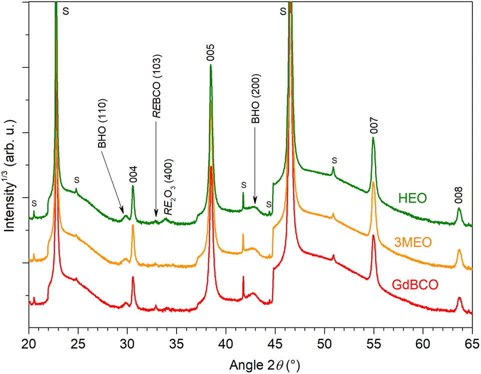 | ||
| Fig. 1 XRD θ–2θ scans of three 12 mol% BHO-containing films: Gd0.2Dy0.2Y0.2Ho0.2Er0.2Ba2Cu3O7−δ (HEO, green), Y0.33Er0.33Ho0.33Ba2Cu3O7−δ (3MEO, orange) and GdBCO (red). Except for a tiny (103) peak, only (00l) reflections are visible for the REBCO phase. BHO and RE2O3 reflections are indicated as well; S: substrate and setup-related peak. | ||
2.2. Superconducting properties
Fig. 2 compares the films' magnetic field dependencies of Jc at 77 K and 30 K as well as the corresponding pinning force densities (Fp). At 77 K, 2MEO shows the largest Jsfc with 6.9 MA cm−2, while HEO reaches 3.5 MA cm−2, which is slightly below the values of other REBCO films but still remarkable. However, all samples, including HEO, show rather similar Jc values for medium applied fields around 1 T. The Fp curves at 77 K show that GdBCO presents the largest maximum value of ∼13 GN m−3. This is closely followed by 2MEO with ∼11.5 GN m−3 and HEO with ∼10 GN m−3, both surpassing the value of 3MEO, which is mainly due to its lower Tc value. | ||
| Fig. 2 Comparison of the magnetic field dependencies of the critical current density Jc and corresponding pinning force density Fp for B‖c at 77 K and 30 K. R(T) curves of the samples are included as an inset in the bottom right panel. | ||
The situation drastically changes at 30 K. There, 3MEO shows the largest values of Jc and Fp. The 2MEO film has the second-largest values of both quantities, while the HEO film has lower values than these two, yet, is still overcoming the values of GdBCO. The slopes of Fp(B) at the maximum magnetic field available (14 T), however, indicate that the HEO sample might overtake the MEO samples at even higher fields (and or lower temperatures). These results suggest that by mixing different REBCO, i.e., by creating ME or HE REBCO films, certain types of pinning centers (i.e. point-like defects with associated strain states) are introduced that are more effective at lower temperatures and higher fields, and HE mixing might be a way to even further improve especially the high-field properties. Furthermore, not all mixtures seem to work equally well, and simply mixing more and more REBCO phases will not automatically lead to better results. It is rather a matter of selecting the appropriate compounds to be mixed. For example, the mixture of the chosen three components seems more effective at medium fields than the mixture of five, and this is probably also a result of the compound selection. YBCO, ErBCO and HoBCO are compounds with similar RE3+ ion sizes and CSD growth conditions. Therefore, when selecting the mixture's growth parameters, they will be near the ones for every individual phase favoring the final quality of the MEO film. In the case of the HEO film, the RE3+ ion size of GdBCO is quite different from the rest of the constituents, and so are the growth parameters. These differences certainly define the efficiency of ME or HE mixing in REBCO films. Therefore, it is crucial to make an appropriate selection of the compounds in the mixture to optimize the final properties of the films. Further important factors for the final performance of MEO and HEO films are the average RE ion size and its variance.19,42 This aspect has not been considered in this work, yet should be studied in detail for HE REBCO films (and bulks) in future work.
The superconducting properties presented above in Fig. 2 and the Tc values of the films are summarised in Table 1. Tc of the HEO sample reaches 91.9 K, which is very similar to the 2MEO film, whereas GdBCO shows 94.4 K and the 3MEO film has a somewhat lower Tc of 89.2 K, which may be due to the highest Y content in this sample of 50%. ΔTc was in the range of 1.0–1.2 K for the four different samples. In general, our pure YBCO films have lower Tc values than REBCO films with lanthanoid RE elements.41 So, the final Tc value can be considered an average of the ones of the REBCO compounds included in the mixture at the chosen deposition conditions. This averaging effect was already described for Y1−xGdxBa2Cu3O7−δ MEO films.14
| Compound | Tc (K) | Jsfc (77 K) (MA cm−2) | Jc (3 T, 30 K) (MA cm−2) |
|---|---|---|---|
| GdBCO | 94.4 | 5.3 | 3.7 |
| 2MEO | 91.8 | 6.9 | 4.7 |
| 3MEO | 89.2 | 5.5 | 5.7 |
| HEO | 91.9 | 3.5 | 4.1 |
2.3. Microstructural characterization by TEM
To understand the evolution of the superconducting properties with temperature and to explain the possible changes in the pinning landscape in the HEO films with respect to the standard REBCO nanocomposites, we carried out a comprehensive TEM study of the GdBCO, MEO (i.e. 3MEO) and HEO BHO-nanocomposite films to investigate the film quality and to compare the RE distribution. Note that the GdBCO film investigated by TEM was grown on a LaAlO3(001) (LAO) instead of a SrTiO3(001) (STO) single-crystalline substrate (under otherwise same conditions, see experimental section). The different substrates should not influence the Gd distribution in GdBCO but could lead to differences in the defect structure (e.g., in the concentration of misoriented GdBCO grains) between LAO and STO. Due to the possible influence of the substrate material, we do not compare the defect structure of the MEO/HEO and GdBCO films but focus only on the RE distributions.Microstructural analyses by STEM are presented in the following. In general, low-magnification LAADF-STEM overview images reveal that the HEO film can be grown with a rather homogeneous thickness and quality (∼220 nm, Fig. 3a). The GdBCO film has a thickness of ∼200 nm (Fig. 3b). The dark regions in Fig. 3b result from FIB-induced damage during TEM sample preparation and are not present in the as-deposited GdBCO film. Randomly oriented BHO nanoparticles appear dark in LAADF-STEM imaging (some particles are encircled in Fig. 3a and b with a blue line, and are marked in Fig. 3d with solid arrows). In contrast, BHO particles close to a zone-axis orientation appear bright. This is caused by more intense Bragg scattering close to a zone-axis orientation, which leads to a higher intensity on the LAADF detector. These particles are in epitaxial alignment with respect to the substrate close to the film/substrate interface (dashed arrows in Fig. 3d). At higher magnification (Fig. 3c–e), stacking faults (SFs) appear as dark, horizontal lines in the LAADF-STEM images. A high, medium, and low SF density is observed for MEO (Fig. 3d), HEO (Fig. 3e), and GdBCO (Fig. 3c), respectively. Such stacking faults strongly influence the pinning behavior for fields close to the ab-planes (not shown here). The strong diffraction-contrast variations in Fig. 3d may be caused by a slightly larger sample thickness of the MEO film. As a result, more BHO particles are imaged simultaneously along the viewing/beam direction in the thicker TEM sample, leading to more complex image contrasts. In addition, intensity variations are observed along the [001] direction (e.g. green arrow in Fig. 3d). These defects are probably 〈110〉-type twin-boundaries, which are disrupted by the presence of nanoparticles and stacking faults.43
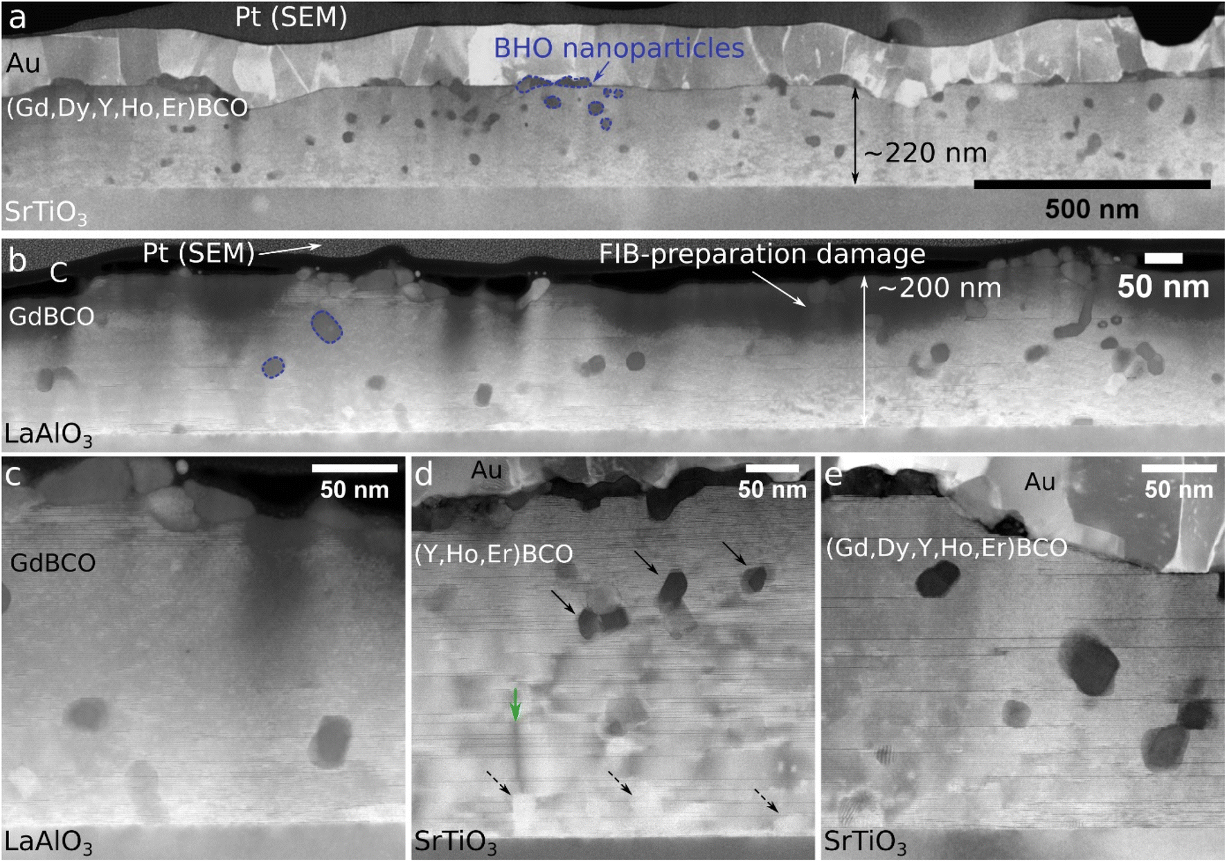 | ||
| Fig. 3 Representative LAADF-STEM overview images of the investigated CSD-grown REBCO + 12 mol% BaHfO3 nanocomposite films. The large field-of-view LAADF-STEM images of (a) HEO and (b) GdBCO show that the HEO film can be grown with comparable film quality as single-RE films (albeit the GdBCO film shown here was grown on LAO). The BaHfO3 nanoparticles (a few particles are marked with dashed blue lines in (a and b)) appear mostly dark in random orientation in the film (solid arrows in (d)). They appear bright in epitaxial orientation with respect to the substrate (dashed arrows in (d)). The dark regions near the surface for (b) GdBCO stem from FIB-induced preparation damage (amorphization of GdBCO). The higher magnification LAADF-STEM images of (c) GdBCO, (d) MEO, and (e) HEO reveal stacking faults, which appear as dark, horizontal lines. The film is protected during FIB preparation by an evaporated C layer and an electron-beam deposited Pt/C layer, here denoted as “Pt (SEM)”. | ||
High-resolution HAADF-STEM images of the film/substrate interface reveal epitaxial growth of the MEO (Fig. 4a) and the HEO film (Fig. 4b) on STO with the orientation (001)[100]REBCO‖(001)[100]STO. The dark, horizontal lines are SFs, i.e., extra CuO planes. The resulting double CuO chains are found in the REBa2Cu4O8 (RE124) or RE2Ba4Cu7O15−δ (RE247) phases, which are structurally related to REBCO.44 A higher SF density is observed for MEO (Fig. 4a) compared to HEO (Fig. 4b) as already observed in the lower-magnification STEM images (Fig. 3d and e). The associated b/2- or [010]/2-shift of the REBCO unit cell at a SF45 can lead to a glide (Fig. 4c, interrupted vertical lines) or mirror symmetry (Fig. 4d, continuous vertical line) at the SF (marked by arrows), depending on the orientation of the orthorhombic REBCO structure.43,46 The [100] or [010] orientation can switch along the [001] direction43,46–49 which can be observed in Fig. 4c and d. These images are color-coded and magnified from the overview image shown in Fig. 4a. All other visible SFs in Fig. 4a and b show glide symmetry.
 | ||
| Fig. 4 Representative high-resolution HAADF-STEM images of the (a) MEO and (b) HEO film near the film/substrate interface. In general, cube-on-cube epitaxial growth is observed for both films, which is also visible in the magnified insets in (d) and (e). The dark horizontal lines correspond to stacking faults (extra CuO planes). The arrows in (b) point towards small, damaged regions, probably caused by FIB preparation or TEM-sample degradation. The magnified insets from (a) shown in the color-coded high-resolution HAADF-STEM images (c) and (d) show stacking faults with glide and mirror symmetry, respectively. (e) Magnified view from (b) showing a substrate step (marked by a vertical arrow) and a small epitaxially grown BaHfO3 nanoparticle. | ||
One can observe small disturbed regions in the REBCO films (cf. arrows in Fig. 4b), which are probably caused by FIB-induced damage during sample preparation. Alternatively, these defects could also be attributed to a degradation of the thin REBCO TEM sample,50,51 resulting in the formation of RE124-type defects.50 These cause a local buckling of the REBCO structure similar to the shown defects. We note that the investigated TEM samples were directly observed in the TEM after FIB preparation with a ∼20 min exposure to air during the sample transfer between the microscopes. Atomically sharp film/substrate interfaces with cube-on-cube growth for the MEO and the HEO film are observed at higher magnification (Fig. 4d and e). A syntaxially grown BHO particle is visible in Fig. 4e with the orientation (001)[100]BHO‖(001)[100]REBCO. The growth of BHO starts at the first CuO plane with dark contrast after one unit cell of REBCO, which was also observed by Molina-Luna et al.52 In addition, an atomic step is visible at the substrate surface (marked by a vertical arrow). These steps are compensated by a SF or – as shown here – by BHO formation.
We use the chemical sensitivity of HAADF-STEM Z-contrast imaging53 to approximate the composition by evaluating the HAADF-STEM intensities in undisturbed regions of the REBCO films (Fig. 5). The as-acquired, unfiltered HAADF-STEM images are shown in Fig. 5a–c for GdBCO, MEO, and HEO, respectively. The marked regions (about 10 nm by 10 nm) were used for further analysis (Fig. 5d–f). The as-acquired HAADF-STEM images show low-frequency intensity modulations (especially in Fig. 5c) attributed to FIB-preparation artifacts and possible contamination layers on the TEM sample surface. These unwanted background-intensity modulations were removed in Fig. 5d–f by subtracting a background image. The latter is created by blurring an HAADF-STEM image with an anisotropic-diffusion filter until the atomic-structure details completely vanish. Line profiles along the [001] direction were then extracted from the background-corrected images (marked regions in Fig. 5 d–f). We averaged the image intensities over almost the entire image width (along the [100] or [010] direction) to increase the signal-to-noise ratio. In Fig. 5d, a vertical shift of the GdBCO structure due to sample drift during STEM-image acquisition is visible roughly in the middle of the image. Therefore, only the left half of the image was averaged.
 | ||
| Fig. 5 Comparison of HAADF-STEM-intensity line profiles for GdBCO (left column), MEO (middle column) and HEO (right column). (a–c) Raw HAADF-STEM overview images with the ∼100 nm2 analyzed regions in (d–f) marked by yellow squares. (d–f) Background-subtracted representative, defect-free REBCO regions used for the analysis of (g–i) HAADF-STEM-intensity line profiles along the [001] direction. The line scans were horizontally averaged in the marked regions and the arrows indicate the line-profile direction (bottom to top). The intensity values were normalized between the minimum and maximum values for each profile. The horizontal lines mark the average intensities for the REs (dashed blue), Ba (dotted green), and Cu (solid red) as determined by evaluating the peak (RE and Ba)/trough (Cu) intensities. The shaded regions correspond to the standard deviation of the average values. | ||
The extracted line profiles (Fig. 5g–i) show the HAADF-STEM intensities of the RE- (highest peaks/blue dashed line), Ba- (second highest peaks/green dotted line), and Cu-planes (intensity minima/solid red line). Contributions from O to the HAADF intensities were neglected, as O is not visible in HAADF-STEM Z-contrast images in combination with heavier elements, which is due to the significant difference in atomic number. For clarity, the intensity values were normalized between the minimum and maximum intensity (0 and 1) in each line profile. The horizontal lines mark the average intensity values Ix (with x = RE, Ba, or Cu) for each element as determined by peak fitting. The shaded regions correspond to the standard deviation of the average values Ix.
The HAADF-STEM images were taken in different microscope sessions with different detector bias and gain settings. The latter affect the intensity ratios between the peaks. To evaluate the intensities Ix, we use the ratio

| Intensity | GdBCO | Y0.33Er0.33Ho0.33BCO (3MEO) | Gd0.2Dy0.2Y0.2Ho0.2Er0.2BCO (HEO) |
|---|---|---|---|
| IRE | 0.942 ± 0.012 | 0.960 ± 0.009 | 0.939 ± 0.014 |
| IBa | 0.669 ± 0.006 | 0.839 ± 0.014 | 0.777 ± 0.009 |
| ICu | 0.049 ± 0.008 | 0.117 ± 0.023 | 0.028 ± 0.006 |
| Rexp | 0.31 ± 0.01 | 0.14 ± 0.02 | 0.18 ± 0.02 |
For the qualitative HAADF-STEM composition analysis above, the HAADF-STEM intensity was averaged along the [100] or [010] directions to increase the signal-to-noise ratio. In this way, however, one loses the information about changes in the RE composition along the [100]/[010] direction. Hence, additional chemical analyses by STEM-EDXS were performed for MEO (Fig. 6a) and HEO (Fig. 6b) to overcome this problem. A relatively small region of a few nm2 was mapped with high spatial sampling to resolve the RE planes. A few SFs are visible in the field-of-view for HEO (Fig. 6b, arrows). In general, the RE-elemental maps for both MEO and HEO show a homogenous RE-intensity distribution along the [100]/[010] direction. The horizontally aligned RE planes are vertically separated by the lattice parameter c ≈ 1.17 nm as verified by the crystal structure shown in Fig. 6c for the HEO sample. From this observation and the analysis shown in Fig. 5, we conclude that the REs for MEO and HEO are homogeneously distributed within the REBCO films, i.e. the terms HEO and MEO are justified due to the apparent absence of clustering. This is in contrast to the findings of Araki et al.,54 who observed nano-clusters of the added RE's called clustered atom-replaced structure (CARS) in their TFA-MOD-grown REBCO films.
 | ||
| Fig. 6 High-resolution chemical analysis of (a) MEO and (b) HEO films by STEM-EDXS. The dashed lines mark the film/substrate interfaces. The RE signals are homogeneously distributed in the film for both samples as visible by the horizontal lines corresponding to the RE planes in all RE maps (vertical lattice-plane spacing about 1.17 nm). A crystal-structure model of Gd0.2Dy0.2Y0.2Ho0.2Er0.2BCO viewed along the [100] zone-axis is shown in (c). The structure model was created with VESTA.56 (a) At the interface, a small Ti signal is found (white arrow) in the REBCO region, which could be caused by Ti diffusion from SrTiO3 into REBCO. In (b), some stacking faults are visible and marked by arrows. The X-ray transitions used as chemical signals are given for each element above the corresponding map. | ||
Regarding the other elements, a slight Ba depletion/O enhancement is observed in Fig. 6a at the RE planes, as expected for the REBCO crystal structure (Fig. 6c). More O is measured near RE due to the CuO2 planes surrounding the RE compared to the CuO ribbons near the Ba sites. The signal in the Cu map is artificially increased by stray X-rays from the Cu-TEM grid, which increases the Cu signal in the RE planes. Therefore, the Cu map cannot be easily interpreted. A weak Ti signal at the film/substrate interface (dashed, white line) is visible (see arrow in the Ti map in Fig. 6a), which slowly decays along the c-direction. This may be caused by Ti diffusion from STO into REBCO, which was already observed by us40 and other groups.52,55
The EDXS spectra from the REBCO region were summed up and quantified to get an approximation for the average film composition (Table 3). The results agree with the expected film composition within the experimental errors associated with standardless EDXS quantification. The only exception is the Gd content, which is higher than the nominal content in the analyzed region. However, this effect was not observed in other EDXS datasets from the same sample (not shown here). Therefore, the increased Gd concentration is probably an artifact of limited X-ray-count statistics in the dataset.
| Element | MEO/at% | HEO/at% |
|---|---|---|
| Ba (Lα) | 16.6 (15.4) | 14.9 (15.4) |
| Cu (Lα) | 24.5 (23.1) | 24.5 (23.1) |
| O (Kα) | 50.6 (54.0) | 52.2 (54.0) |
| Gd (Lα) | — | 2.4 (1.5) |
| Dy (Lα) | — | 1.7 (1.5) |
| Y (Kα) | 2.3 (2.5) | 1.1 (1.5) |
| Ho (Lα) | 3.2 (2.5) | 1.7 (1.5) |
| Er (Lα) | 2.8 (2.5) | 1.5 (1.5) |
3. Conclusion
In this work, we present the first successful synthesis of High-Entropy (HE) superconducting REBCO nanocomposite films by CSD. These films contain 12 mol% BHO nanoparticles. After growth optimization, we obtained highly c-axis-textured Gd0.2Dy0.2Y0.2Ho0.2Er0.2Ba2Cu3O7−δ films on STO substrates. Both Tc and Jsfc at 77 K, 91.9 K and 3.5 MA cm−2, respectively, are similar to other, more standard single-RE REBCO films. The properties of this HEO film improved significantly at 30 K with respect to the other REBCO films. However, Tc and Jc(B) are still not exceeding those of the medium-entropy film Y0.33Er0.33Ho0.33Ba2Cu3O7−δ (3MEO), while promising better performance at high fields and lowest temperatures. There could be several reasons for this difference but selecting the appropriate REBCO compounds is crucial. It is not only a matter of mixing but mixing the most pertinent compounds to optimize the properties of the final films.An extensive TEM study was carried out for these films to investigate the microstructure. Here, we observed a good film quality for HEO Gd0.2Dy0.2Y0.2Ho0.2Er0.2Ba2Cu3O7−δ, comparable to GdBCO with homogeneously distributed BHO nanoparticles. High-resolution HAADF-STEM and STEM-EDXS analyses showed a homogeneous distribution of REs for Y0.33Er0.33Ho0.33Ba2Cu3O7−δ and Gd0.2Dy0.2Y0.2Ho0.2Er0.2Ba2Cu3O7−δ at the atomic level for the chosen REBCO fabrication method, hence a true HEO, respectively MEO, compound.
4. Experimental methods
4.1 Sample preparation
The procedure to prepare the solutions used for the deposition of the HE REBCO films consists of two main steps: preparing the individual solutions of every REBCO used in the mixture and mixing them according to the desired stoichiometry of the HEO films. The preparation routine for the different REBCO-TFA solutions is explained in detail in ref. 41. In short, the RE, Ba, and Cu precursor salts (acetates; purity >99.99%, Alfa Aesar) and the hafnium precursor salt (hafnium(IV) 2,4-pentanedionate (Hf(acac)4); 97+%, Alfa Aesar) are put together in a mixture of deionized water and trifluoroacetic acid (99.5+%, Alfa Aesar) with a stoichiometric ratio of 1![[thin space (1/6-em)]](https://www.rsc.org/images/entities/char_2009.gif) :2:3 for RE, Ba, and Cu and the required amount of Hf(acac)4 for a 12 mol% BHO concentration with regard to RE. Using a rotary evaporator, this mixture is dried and then re-dissolved in anhydrous methanol (99.9%). The volume of the final solution is adjusted with methanol for a final RE cation concentration of 0.25 mol l−1.
:2:3 for RE, Ba, and Cu and the required amount of Hf(acac)4 for a 12 mol% BHO concentration with regard to RE. Using a rotary evaporator, this mixture is dried and then re-dissolved in anhydrous methanol (99.9%). The volume of the final solution is adjusted with methanol for a final RE cation concentration of 0.25 mol l−1.
These mixed solutions are deposited on 10 × 10 mm2 (100)-oriented SrTiO3 single-crystal substrates via spin coating (6000 rpm for 30 s). The as-deposited samples are then placed in a tubular furnace for pyrolysis and film growth (including the oxygenation process). The thermal profiles used in this work are detailed in ref. 57. The GdBCO + BHO sample used as a reference in the TEM section was grown on a LaAlO3 single-crystal substrate under otherwise similar conditions. This type of nanocomposite film shows certain growth differences between LAO and STO, in particular a larger amount of misoriented grains on LAO, specially, near the interface. However, the fact that this sample is not used to compare the microstructure but only the distribution of the RE3+ ions makes these possible changes in the microstructure irrelevant for our study.
4.2 Characterisation of the films
Crystallographic orientation and crystallinity of the films were analyzed by X-ray diffraction (XRD) using a Bruker D8 diffractometer with Cu Kα radiation. Self-field critical current density, Jsfc, at 77 K was measured inductively with a Cryoscan (THEVA, 50 μV criterion, corresponding to 1 μV cm−1 in transport measurements). The values of Jc at different magnetic fields, Jc(B), were measured on a 14-T Quantum Design Physical Property Measurement System (PPMS) with a 1 μV cm−1 criterion. Also, the critical temperature Tc (defined as Tc,90, i.e. the temperature at which the resistance is 90% of the value above the transition) was measured by transport in the same PPMS. The transport data were measured on 10–20 μm wide and 1 mm long tracks prepared by photolithography with wet-chemical etching.4.3 TEM measurements
A FEI Strata 400S focused-ion-beam (FIB)/scanning electron microscope (SEM) system was used to prepare cross-section samples for scanning transmission electron microscopy (STEM) by an in situ lift-out technique.58 A low Ga+-ion energy of 2 keV was used for the final polishing step to minimize amorphous surface layers on the TEM samples.59,60 High- and low-angle annular dark-field (HAADF/LAADF) STEM images with inner collection semi-angles of 40 mrad/11.5 mrad, respectively, were acquired with a FEI Titan3 80–300 transmission electron microscope operated at 300 kV with a spherical aberration coefficient Cs = 1.2 mm for the probe-forming lens. A probe convergence semi-angle of 9 mrad was used. The signal was collected with a Fischione Model 3000 ADF detector. High-resolution HAADF-STEM images were partly filtered with an average-background subtraction filter61 using the “HRTEM Filter” plugin for DigitalMicrograph.62 A background-intensity image created by image blurring with an anisotropic diffusion filter63 in Fiji64 was used to remove low-frequency background modulations in some images.A FEI Tecnai Osiris operated at 200 kV with ChemiSTEM technology65 was used for chemical analysis with energy-dispersive X-ray spectroscopy (EDXS). A probe convergence semi-angle of 10.7 mrad was used in combination with a numerical spot-size (gun lens) value of 8 (5) to obtain a small probe (<0.4 nm full width at half maximum) with a beam current of about 100 pA. The acquisition was controlled by the Bruker Esprit 1.9 software with drift correction by the simultaneously acquired HAADF-STEM signal (collection semi-angle roughly 53–200 mrad). The acquired STEM-EDXS spectrum images were denoised with principal component analysis66 before extracting the X-ray peak intensities as chemical signals using the HyperSpy Python package.67,68 EDXS quantification was performed with the Bruker Esprit 2.1 software using the standardless Cliff–Lorimer approach.69 The Cu Lα X-ray line was used instead of Cu Kα for quantification of the Cu content to minimize the influence of spurious Cu Kα X-rays from the Cu grid penetrating the thin TEM samples. A correction for X-ray absorption was applied with an assumed sample thickness of 75 nm and a calculated REBCO density of 6.9 g cm−3.
Data availability
All relevant data are included in the paper. Raw data are available from the corresponding authors upon request.Author contributions
P. C. conceptualized the idea, prepared the films and characterized them. L. G. carried out the TEM analysis. M. E. and J. H. participated in the physical characterization of the samples. D. G. and B. H. supervised the work. All authors were involved in writing the original and the revised manuscript.Conflicts of interest
The authors declare no competing interests.Acknowledgements
We acknowledge support by the KIT-Publication Fund of the Karlsruhe Institute of Technology.References
- Y. Shiohara, M. Yoshizumi, Y. Takagi and T. Izumi, Future Prospects of High Tc Superconductors-Coated Conductors and Their Applications, Phys. C, 2013, 484, 1–5, DOI:10.1016/j.physc.2012.03.058.
- D. Larbalestier, A. Gurevich, D. M. Feldmann and A. Polyanskii, High-Tc Superconducting Materials for Electric Power Applications, Nature, 2001, 414(6861), 368–377, DOI:10.1038/35104654.
- X. Obradors and T. Puig, Coated Conductors for Power Applications: Materials Challenges, Supercond. Sci. Technol., 2014, 27(4), 044003, DOI:10.1088/0953-2048/27/4/044003.
- A. Molodyk, S. Samoilenkov, A. Markelov, P. Degtyarenko, S. Lee, V. Petrykin, M. Gaifullin, A. Mankevich, A. Vavilov, B. Sorbom, J. Cheng, S. Garberg, L. Kesler, Z. Hartwig, S. Gavrilkin, A. Tsvetkov, T. Okada, S. Awaji, D. Abraimov, A. Francis, G. Bradford, D. Larbalestier, C. Senatore, M. Bonura, A. E. Pantoja, S. C. Wimbush, N. M. Strickland and A. Vasiliev, Development and Large Volume Production of Extremely High Current Density YBa2Cu3O7 Superconducting Wires for Fusion, Sci. Rep., 2021, 11(1), 2084, DOI:10.1038/s41598-021-81559-z.
- S. Fujita, S. Muto, W. Hirata, T. Yoshida, K. Kakimoto, Y. Iijima, M. Daibo, T. Kiss, T. Okada and S. Awaji, Flux-Pinning Properties of BaHfO3-Doped EuBCO-Coated Conductors Fabricated by Hot-Wall PLD, IEEE Trans. Appl. Supercond., 2019, 29(5), 1–5, DOI:10.1109/TASC.2019.2896535.
- M. Murakami, N. Sakai, T. Higuchi and S. I. Yoo, Melt-Processed Light Rare Earth Element-Ba-Cu-O, Supercond. Sci. Technol., 1996, 9(12), 1015–1032, DOI:10.1088/0953-2048/9/12/001.
- C. Andreouli and A. Tsetsekou, Synthesis of HTSC Re(Y)Ba2Cu3Ox Powders: The Role of Ionic Radius, Phys. C, 1997, 291(3), 274–286, DOI:10.1016/S0921-4534(97)01636-5.
- M. S. Islam and R. C. Baetzold, Atomistic Simulation of Dopant Substitution in YBa2Cu3O7, Phys. Rev. B: Condens. Matter Mater. Phys., 1989, 40(16), 10926–10935, DOI:10.1103/PhysRevB.40.10926.
- J. L. Macmanus-Driscoll, Materials Chemistry and Thermodynamics of REBa2Cu3O7-x, Adv. Mater., 1997, 9(6), 457–473, DOI:10.1002/ADMA.19970090602.
- J. L. MacManus-Driscoll, J. A. Alonso, P. C. Wang, T. H. Geballe and J. C. Bravman, Studies of Structural Disorder in ReBa2Cu3O7-x Thin Films (Re=rare Earth) as a Function of Rare-Earth Ionic Radius and Film Deposition Conditions, Phys. C, 1994, 232(3), 288–308, DOI:10.1016/0921-4534(94)90789-7.
- Y. Yoshida, T. Ozaki, Y. Ichino, Y. Takai, K. Matsumoto, A. Ichinose, M. Mukaida and S. Horii, Progress in Development of Advanced PLD Process for High Jc REBCO Film, Phys. C, 2008, 468(15), 1606–1610, DOI:10.1016/j.physc.2008.05.082.
- P. Cayado, M. Erbe, S. Kauffmann-Weiss, C. Bühler, A. Jung, J. Hänisch and B. Holzapfel, Large Critical Current Densities and Pinning Forces in CSD-Grown Superconducting GdBa2Cu3O7−x-BaHfO3 Nanocomposite Films, Supercond. Sci. Technol., 2017, 30(9), 094007, DOI:10.1088/1361-6668/aa7e47.
- S. H. Wee, A. Goyal, P. M. Martin and L. Heatherly, High In-Field Critical Current Densities in Epitaxial NdBa2Cu3O7−δ Films on RABiTS by Pulsed Laser Deposition, Supercond. Sci. Technol., 2006, 19(8), 865–868, DOI:10.1088/0953-2048/19/8/031.
- P. Cayado, M. Erbe, S. Kauffmann-Weiss, A. Jung, J. Hänisch and B. Holzapfel, Chemical Solution Deposition of Y1−xGdxBa2Cu3O7−δ–BaHfO3 Nanocomposite Films: Combined Influence of Nanoparticles and Rare-Earth Mixing on Growth Conditions and Transport Properties, RSC Adv., 2018, 8(74), 42398–42404, 10.1039/C8RA09188A.
- M. Muralidhar and M. Murakami, Effect of Eu/Gd Ratio on Flux Pinning in (Nd, Eu, Gd)-Ba-Cu-O, Supercond. Sci. Technol., 2000, 13(9), 1315–1321, DOI:10.1088/0953-2048/13/9/306.
- H. Jian, D. Shao, Z. Yang, X. Zhu and Y. Sun, Jc Enhancement and Flux Pinning in Y1-xGdxBCO and (Gd,Eu) Codoped Y0.9-yEuyGd0.1BCO Thin Films by TFA-MOD, Phys. C, 2013, 488, 39–45, DOI:10.1016/j.physc.2013.03.001.
- P. Cayado, H. Rijckaert, M. Erbe, M. Langer, A. Jung, J. Hänisch and B. Holzapfel, CSD-Grown Y1−xGd xBa2Cu3O7−δ-BaHfO3 Nanocomposite Films on Ni5W and IBAD Technical Substrates, Nanomaterials, 2019, 10(1), 21, DOI:10.3390/nano10010021.
- C. Cai, J. Hänisch, T. Gemming and B. Holzapfel, Anisotropic Enhancement of Flux Pinning in Mixed Rare Earth 123-Type Thin Films, IEEE Trans. Appl. Supercond., 2005, 15(2), 3738–3741, DOI:10.1109/TASC.2005.849418.
- J. L. MacManus-Driscoll, S. R. Foltyn, B. Maiorov, Q. X. Jia, H. Wang, A. Serquis, L. Civale, Y. Lin, M. E. Hawley, M. P. Maley and D. E. Peterson, Rare Earth Ion Size Effects and Enhanced Critical Current Densities in Y2/3Sm1/3Ba2Cu3O7−x Coated Conductors, Appl. Phys. Lett., 2005, 86(3), 032505, DOI:10.1063/1.1851006.
- P. Cayado, M. Li, M. Erbe, Z. Liu, C. Cai, J. Hänisch and B. Holzapfel, REBCO Mixtures with Large Difference in Rare-Earth Ion Size: Superconducting Properties of Chemical Solution Deposition-Grown Yb1-xSmxBa2Cu3O7-δ Films, R. Soc. Open Sci., 2020, 7(11), 201257, DOI:10.1098/rsos.201257.
- T. J. Haugan, J. C. Tolliver, J. M. Evans and J. W. Kell, Crystal chemical substitutions of YBa2Cu3O7-δ to enhance flux pinning, in Studies of High Temperature Superconductors, ed. A. Narlikar, Nova Science Publishers, 2006, vol. 49 Search PubMed.
- Y. Li and Z.-X. Zhao, Stress-Field Pinning Induced by the Lattice Mismatch in 123 Phase, Phys. C, 2001, 351(1), 1–4, DOI:10.1016/S0921-4534(00)01677-4.
- L. Sun and R. J. Cava, High-Entropy Alloy Superconductors: Status, Opportunities, and Challenges, Phys. Rev. Mater., 2019, 3(9), 090301, DOI:10.1103/PhysRevMaterials.3.090301.
- J. Kitagawa, S. Hamamoto and N. Ishizu, Cutting Edge of High-Entropy Alloy Superconductors from the Perspective of Materials Research, Metals, 2020, 10(8), 1078, DOI:10.3390/met10081078.
- M. C. Gao, D. B. Miracle, D. Maurice, X. Yan, Y. Zhang and J. A. Hawk, High-Entropy Functional Materials, J. Mater. Res., 2018, 33(19), 3138–3155, DOI:10.1557/jmr.2018.323.
- A. Sarkar, Q. Wang, A. Schiele, M. R. Chellali, S. S. Bhattacharya, D. Wang, T. Brezesinski, H. Hahn, L. Velasco and B. Breitung, High-Entropy Oxides: Fundamental Aspects and Electrochemical Properties, Adv. Mater., 2019, 31(26), 1806236, DOI:10.1002/adma.201806236.
- P. Koželj, S. Vrtnik, A. Jelen, S. Jazbec, Z. Jagličić, S. Maiti, M. Feuerbacher, W. Steurer and J. Dolinšek, Discovery of a Superconducting High-Entropy Alloy, Phys. Rev. Lett., 2014, 113(10), 107001, DOI:10.1103/PhysRevLett.113.107001.
- R. Sogabe, Y. Goto and Y. Mizuguchi, Superconductivity in REO0.5F0.5BiS2 with High-Entropy-Alloy-Type Blocking Layers, Appl. Phys. Express, 2018, 11(5), 053102, DOI:10.7567/APEX.11.053102.
- T. Ying, T. Yu, Y. S. Shiah, C. Li, J. Li, Y. Qi and H. Hosono, High-Entropy van Der Waals Materials Formed from Mixed Metal Dichalcogenides, Halides, and Phosphorus Trisulfides, J. Am. Chem. Soc., 2021, 143(18), 7042–7049, DOI:10.1021/jacs.1c01580.
- Y. Mizuguchi, Superconductivity in High-Entropy-Alloy Telluride AgInSnPbBiTe5, J. Phys. Soc. Jpn., 2019, 88(12), 124708, DOI:10.7566/JPSJ.88.124708.
- A. Yamashita, R. Jha, Y. Goto, T. D. Matsuda, Y. Aoki and Y. Mizuguchi, An Efficient Way of Increasing the Total Entropy of Mixing in High-Entropy-Alloy Compounds: A Case of NaCl-Type (Ag,In,Pb,Bi)Te1-xSex (x = 0.0, 0.25, 0.5) Superconductors, Dalton Trans., 2020, 49(26), 9118–9122, 10.1039/d0dt01880e.
- A. Yamashita, T. D. Matsuda and Y. Mizuguchi, Synthesis of New High-Entropy Alloy-Type Nb3 (Al, Sn, Ge, Ga, Si) Superconductors, J. Alloys Compd., 2021, 868, 159233, DOI:10.1016/j.jallcom.2021.159233.
- M. R. Kasem, A. Yamashita, T. Hatano, K. Sakurai, N. Oono-Hori, Y. Goto, O. Miura and Y. Mizuguchi, Anomalous Broadening of Specific Heat Jump at Tc in High-Entropy-Alloy-Type Superconductor TrZr2, Supercond. Sci. Technol., 2021, 34(12), 6, DOI:10.1088/1361-6668/ac2554.
- Y. Shukunami, A. Yamashita, Y. Goto and Y. Mizuguchi, Synthesis of RE123 High-Tc Superconductors with a High-Entropy-Alloy-Type RE Site, Phys. C, 2020, 572, 1353623, DOI:10.1016/j.physc.2020.1353623.
- A. Yamashita, Y. Shukunami and Y. Mizuguchi, Improvement of Critical Current Density of REBa2Cu3O7-δ by Increase in Configurational Entropy of Mixing, R. Soc. Open Sci., 2022, 9(3), 211874, DOI:10.1098/rsos.211874.
- K. Wang, Q. Hou, A. Pal, H. Wu, J. Si, J. Chen, S. Yu, Y. Chen, W. Lv, J. Y. Ge, S. Cao, J. Zhang and Z. Feng, Structural and Physical Properties of High-Entropy REBa2Cu3O7-δ Oxide Superconductors, J. Supercond. Novel Magn., 2021, 34(5), 1379–1385, DOI:10.1007/s10948-021-05855-5.
- A. Yamashita, K. Hashimoto, S. Suzuki, Y. Nakanishi, Y. Miyata, T. Maeda and Y. Mizuguchi, Fabrication of High-Entropy REBa2Cu3O7-δ Thin Films by Pulsed Laser Deposition, Jpn. J. Appl. Phys., 2022, 61(5), 050905, DOI:10.35848/1347-4065/ac5b39.
- A. R. Mazza, X. Gao, D. J. Rossi, B. L. Musico, T. W. Valentine, Z. Kennedy, J. Zhang, J. Lapano, V. Keppens, R. G. Moore, M. Brahlek, C. M. Rost and T. Z. Ward, Searching for Superconductivity in High Entropy Oxide Ruddlesden–Popper Cuprate Films, J. Vac. Sci. Technol., A, 2022, 40(1), 013404, DOI:10.1116/6.0001441.
- A. Gupta, R. Jagannathan, E. I. Cooper, E. A. Giess, J. I. Landman and B. W. Hussey, Superconducting Oxide Films with High Transition Temperature Prepared from Metal Trifluoroacetate Precursors, Appl. Phys. Lett., 1988, 52(24), 2077–2079, DOI:10.1063/1.99752.
- M. Erbe, J. Hänisch, R. Hühne, T. Freudenberg, A. Kirchner, L. Molina-Luna, C. Damm, G. Van Tendeloo, S. Kaskel, L. Schultz and B. Holzapfel, BaHfO3 Artificial Pinning Centres in TFA-MOD-Derived YBCO and GdBCO Thin Films, Supercond. Sci. Technol., 2015, 28(11), 114002, DOI:10.1088/0953-2048/28/11/114002.
- M. Erbe, P. Cayado, W. Freitag, K. Ackermann, M. Langer, A. Meledin, J. Hänisch and B. Holzapfel, Comparative Study of CSD-Grown REBCO Films with Different Rare Earth Elements: Processing Windows and Tc, Supercond. Sci. Technol., 2020, 33(9), 094002, DOI:10.1088/1361-6668/ab9aa0.
- J. L. MacManus-Driscoll, S. R. Foltyn, Q. X. Jia, H. Wang, A. Serquis, B. Maiorov, L. Civale, Y. Lin, M. E. Hawley, M. P. Maley and D. E. Peterson, Systematic Enhancement of In-Field Critical Current Density with Rare-Earth Ion Size Variance in Superconducting Rare-Earth Barium Cuprate Films, Appl. Phys. Lett., 2004, 84(26), 5329–5331, DOI:10.1063/1.1766394.
- V. Rouco, A. Palau, R. Guzman, J. Gazquez, M. Coll, X. Obradors and T. Puig, Role of Twin Boundaries on Vortex Pinning of CSD YBCO Nanocomposites, Supercond. Sci. Technol., 2014, 27(12), 125009, DOI:10.1088/0953-2048/27/12/125009.
- K. Yvon and M. François, Crystal Structures of High-Tc Oxides, Z. Phys. B: Condens. Matter, 1989, 76(4), 413–444, DOI:10.1007/BF01307892.
- H. W. Zandbergen, R. Gronsky, K. Wang and G. Thomas, Structure of (CuO)2 Double Layers in Superconducting YBa2Cu3O7, Nature, 1988, 331(6157), 596–599, DOI:10.1038/331596a0.
- J. Gazquez, R. Guzman, R. Mishra, E. Bartolomé, J. Salafranca, C. Magén, M. Varela, M. Coll, A. Palau, S. M. Valvidares, P. Gargiani, E. Pellegrin, J. Herrero-Martin, S. J. Pennycook, S. T. Pantelides, T. Puig and X. Obradors, Emerging Diluted Ferromagnetism in High-Tc Superconductors Driven by Point Defect Clusters, Adv. Sci., 2016, 3(6), 1500295, DOI:10.1002/advs.201500295.
- H. Zhang, N. Gauquelin, G. A. Botton and J. Y. T. Wei, Attenuation of Superconductivity in Manganite/Cuprate Heterostructures by Epitaxially-Induced CuO Intergrowths, Appl. Phys. Lett., 2013, 103(5), 052606, DOI:10.1063/1.4813840.
- A. Palau, F. Vallès, V. Rouco, M. Coll, Z. Li, C. Pop, B. Mundet, J. Gàzquez, R. Guzman, J. Gutierrez, X. Obradors and T. Puig, Disentangling Vortex Pinning Landscape in Chemical Solution Deposited Superconducting YBa2Cu3O7-x Films and Nanocomposites, Supercond. Sci. Technol., 2018, 31(3), 034004, DOI:10.1088/1361-6668/aaa65e.
- V. Pinto, A. Vannozzi, A. Angrisani Armenio, F. Rizzo, A. Masi, A. Santoni, A. Meledin, F. M. Ferrarese, S. Orlanducci and G. Celentano, Chemical Solution Deposition of YBCO Films with Gd Excess, Coatings, 2020, 10(9), 860, DOI:10.3390/coatings10090860.
- H. W. Zandbergen, ABa2Cu4O8 and ABa2Cu5O10 Formed by Intercalation in ABa2Cu3O7 at 20°C in Air, Phys. C, 1992, 193(3), 371–384, DOI:10.1016/0921-4534(92)90959-G.
- N. D. Zakharov, G. Kästner, D. Hesse and M. Lorenz, Observation of Cu Vacancies and Their Ordering in YBa2Cu4O8, Appl. Phys. Lett., 1996, 69(8), 1151–1153, DOI:10.1063/1.117088.
- L. Molina-Luna, M. Duerrschnabel, S. Turner, M. Erbe, G. T. Martinez, S. V. Aert, B. Holzapfel and G. V. Tendeloo, Atomic and Electronic Structures of BaHfO3-Doped TFA-MOD-Derived YBa2Cu3O7-δ Thin Films, Supercond. Sci. Technol., 2015, 28(11), 115009, DOI:10.1088/0953-2048/28/11/115009.
- S. J. Pennycook, Z-Contrast STEM for Materials Science, Ultramicroscopy, 1989, 30(1), 58–69, DOI:10.1016/0304-3991(89)90173-3.
- T. Araki, M. Hayashi, H. Ishii, D. Yokoe, R. Yoshida, T. Kato, G. Nishijima and A. Matsumoto, Clustered Atom-Replaced Structure in Single-Crystal-like Metal Oxide, Supercond. Sci. Technol., 2018, 31(6), 065008, DOI:10.1088/1361-6668/aabb4b.
- T. Nakamura and M. I. M. Iiyama, Characterization of Interdiffusion in SrTiO3/YBa2Cu3O7-x Multilayers by In Situ Auger Electron Spectroscopy, Jpn. J. Appl. Phys., 1995, 34(9R), 4765, DOI:10.1143/JJAP.34.4765.
- K. Momma and F. Izumi, VESTA 3 for Three-Dimensional Visualization of Crystal, Volumetric and Morphology Data, J. Appl. Crystallogr., 2011, 44(6), 1272–1276, DOI:10.1107/S0021889811038970.
- M. Erbe, J. Hänisch, T. Freudenberg, A. Kirchner, I. Mönch, S. Kaskel, L. Schultz and B. Holzapfel, Improved REBa2Cu3O7−x (RE = Y, Gd) Structure and Superconducting Properties by Addition of Acetylacetone in TFA-MOD Precursor Solutions, J. Mater. Chem. A, 2014, 2(14), 4932–4944, 10.1039/C3TA15243J.
- R. M. Langford and C. Clinton, In Situ Lift-out Using a FIB-SEM System, Micron, 2004, 35(7), 607–611, DOI:10.1016/j.micron.2004.03.002.
- J. Mayer, L. A. Giannuzzi, T. Kamino and J. Michael, TEM Sample Preparation and FIB-Induced Damage, MRS Bull., 2007, 32(5), 400–407, DOI:10.1557/mrs2007.63.
- M. Schaffer, B. Schaffer and Q. Ramasse, Sample Preparation for Atomic-Resolution STEM at Low Voltages by FIB, Ultramicroscopy, 2012, 114, 62–71, DOI:10.1016/j.ultramic.2012.01.005.
- R. Kilaas, Optimal and Near-Optimal Filters in High-Resolution Electron Microscopy, J. Microsc., 1998, 190(1–2), 45–51, DOI:10.1046/j.1365-2818.1998.3070861.x.
- D. R. G. Mitchell and B. Schaffer, Scripting-Customised Microscopy Tools for Digital Micrograph™, Ultramicroscopy, 2005, 103(4), 319–332, DOI:10.1016/j.ultramic.2005.02.003.
- D. Tschumperle and R. Deriche, Vector-Valued Image Regularization with PDEs: A Common Framework for Different Applications, IEEE Trans. Pattern Anal. Mach. Intell., 2005, 27(4), 506–517, DOI:10.1109/TPAMI.2005.87.
- J. Schindelin, I. Arganda-Carreras, E. Frise, V. Kaynig, M. Longair, T. Pietzsch, S. Preibisch, C. Rueden, S. Saalfeld, B. Schmid, J. Y. Tinevez, D. J. White, V. Hartenstein, K. Eliceiri, P. Tomancak and A. Cardona, Fiji: An Open-Source Platform for Biological-Image Analysis, Nat. Methods, 2012, 9(7), 676–682, DOI:10.1038/nmeth.2019.
- P. Schlossmacher, D. O. Klenov, B. Freitag and H. S. von Harrach, Enhanced Detection Sensitivity with a New Windowless XEDS System for AEM Based on Silicon Drift Detector Technology, Microsc. Today, 2010, 18(4), 14–20, DOI:10.1017/s1551929510000404.
- I. T. Jolliffe and J. Cadima, Principal Component Analysis: A Review and Recent Developments, Philos. Trans. R. Soc., A, 2016, 374(2065), 20150202, DOI:10.1098/rsta.2015.0202.
- F. d. l. Peña, T. Ostasevicius, V. T. Fauske, P. Burdet, P. Jokubauskas, M. Nord, M. Sarahan, E. Prestat, D. N. Johnstone, J. Taillon, J. Caron, T. Furnival, K. E. MacArthur, A. Eljarrat, S. Mazzucco, V. Migunov, T. Aarholt, M. Walls, F. Winkler, G. Donval, B. Martineau, A. Garmannslund, L.-F. Zagonel and I. Iyengar, Electron Microscopy (Big and Small) Data Analysis With the Open Source Software Package HyperSpy, Microsc. Microanal., 2017, 23(S1), 214–215, DOI:10.1017/S1431927617001751.
- F. d. l. Peña, E. Prestat, V. T. Fauske, P. Burdet, T. Furnival, P. Jokubauskas, J. Lähnemann, M. Nord, T. Ostasevicius, K. E. MacArthur, D. N. Johnstone, M. Sarahan, J. Taillon, T. Aarholt, pquinn-dls, V. Migunov, A. Eljarrat, J. Caron, T. Poon, S. Mazzucco, B. Martineau, actions-user, S. Somnath, T. Slater, C. Francis, N. Tappy, M. Walls, N. Cautaerts, F. Winkler and G. Donval, Hyperspy/Hyperspy: Release v1.6.4, Zenodo, 2021, DOI:10.5281/zenodo.5082777.
- G. Cliff and G. W. Lorimer, The Quantitative Analysis of Thin Specimens, J. Microsc., 1975, 103(2), 203–207, DOI:10.1111/j.1365-2818.1975.tb03895.x.
Footnote |
| † P. C. and L. G. contributed equally in this work. |
| This journal is © The Royal Society of Chemistry 2022 |