
 Open Access Article
 This Open Access Article is licensed under a Creative Commons Attribution-Non Commercial 3.0 Unported Licence
Structural, optical and magnetic properties of pure and 3d metal dopant-incorporated SnO2 nanoparticles†
Supin K Ka,
Anson Georgeb,
Y. Ranjith Kumarac,
Thejas K. K.bc,
Guruprasad Mandald,
Anupama Chanda*e and
M. Vasundhara *abc
*abc
aPolymers and Functional Materials Department, CSIR-Indian Institute of Chemical Technology, Hyderabad 500007, Telangana, India. E-mail: mvas@iict.res.in
bMaterials Science and Technology Division, CSIR-National Institute for Interdisciplinary Science and Technology, Trivandrum 695 019, Kerala, India. E-mail: mvas@niist.res.in
cAcademy of Scientific and Innovative Research (AcSIR), Ghaziabad-201002, India
dCentre for Rural and Cryogenic Technologies, Jadavpur University, Kolkata 700032, India
eDepartment of Physics, Dr Hari Singh Gour Central University, Sagar, 470003, India. E-mail: anupamamatsc@gmail.com
First published on 20th September 2022
Abstract
Dilute magnetic oxide semiconductors doped with transition metals have attracted significant attention both theoretically and experimentally due to their interesting and debatable magnetic behavior. In this work, we investigated the influence of Fe, Co and Ni doping on the structural, optical and magnetic properties of SnO2 nanoparticles, which were produced via a simple sol–gel technique. Raman spectroscopy, XRD, XPS, TEM, FT-IR characterizations were performed to study the crystal structure and morphology of the pure and doped nanoparticles, which confirmed the tetragonal rutile structure of the SnO2 nanoparticles. The XPS analysis revealed the incorporation of divalent dopant ions in the host matrix. The Raman plots indicated the generation of the cassiterite crystal structure, structural disorder and oxygen vacancies in the pure and doped SnO2 nanoparticles. The UV-visible plots indicated a decrease in the bandgap for the doped SnO2 nanoparticles because doping introduced defect levels in the band gap. The photoluminescence study showed the creation of oxygen vacancies due to the doping of different charge states of dopants. The magnetic study based on varying the temperature and field of magnetization revealed the diamagnetic nature of SnO2 at 300 K and 5 K respectively, and the concurrence of ferromagnetic (FM) and paramagnetic (PM) nature in doped SnO2 nanoparticles. The bound polaron model was used to explain the co-existence of FM and PM behavior in all the doped SnO2 nanoparticles.
1 Introduction
Recently, diluted magnetic semiconductors (DMSs), where a minute quantity of magnetic dopants are doped in the parent semiconductor lattice have captivated tremendous interest because of their promising applications in spintronics and spin build electronics.1,2 Spintronic devices use both the charge and spin of electrons, which may revolutionize information technology due to their potential for storage and progressing speed, low electronic power consumption and high integration densities in comparison to the conventional semiconductor devices. However, for practical applications, these devices should exhibit room-temperature ferromagnetism (RTFM). The observation of RTFM in thin films of ZnO and TiO2 has sparked huge interest in oxide-based DMSs.3,4 The occurrence of ferromagnetism in nanocrystalline and nonmagnetic materials is an interesting research field. In oxide semiconductors, the observed ferromagnetic (FM) ordering is called “d0” ferromagnetism, where weak FM ordering is observed with neither the d orbitals nor f orbitals partially filled, have attracted great attention. Oxide-based DMSs have been largely explored both theoretically and experimentally due to their remarkable application in photonic, nanoelectronic, optoelectronic and spintronic devices.Tin oxide (SnO2) has inspired great curiosity among the numerous oxide-based DMSs due to its high transmittance in the visible region, wide bandgap, low electrical resistance, high carrier density, high thermal and chemical stabilities. Among the various n-type semiconductors, SnO2 has a wide bandgap of 3.65 eV at room temperature and finds promising applications in solar cells, gas sensors, transparent conducting electrodes, spintronics, flat panel displays, etc.5–9 It has a structure similar to TiO2 and a lattice in which a high Curie temperature (TC) was first discovered.10 The discovery of RTFM in thin films of Co-doped TiO2 led to the extensive study of rutile-type oxide DMS. The presence of oxygen vacancies (OV) and high carrier density in SnO2 has attracted interest in this material for applications in which a high TC is required. Accordingly, transition metal (TM) ions doping can enhance its magnetic properties, while tuning its optical and electrical properties. Much effort has been devoted to the production of SnO2-based DMSs with RTFM. However, the mechanism of high TC is still under debate, i.e., whether it is due to secondary phases or it is intrinsic to the system. Ogale et al.11 reported a high TC ferromagnetism in thin films of Co-doped SnO2 deposited by pulsed laser deposition; however, paramagnetism was observed in a subsequent study by Fitzgerald et al.12 on similar thin films. Simultaneously, the same authors found RTFM in bulk Mn-, Fe- and Co-doped SnO2 and they attributed this magnetism to the substitution of tin by the dopants despite the presence of a slight amount of impurity.12 Punnoose et al. observed enhanced ferromagnetism in Co-doped SnO2 nanoparticles, where OV played a vital role in obtaining RTFM.13 They also reported the highest TC of 850 K in 1% Fe-doped SnO2 and found that Sn0.95Fe0.05O2 powder was ferromagnetism above the synthesis temperature of 350 °C and showed paramagnetic (PM) behavior above 600 °C.14 Hays et al. studied Fe-doped SnO2 nanoparticles synthesized chemically and they observed a close relation between their structural and magnetic properties.15 Coey et al. observed the FM nature of Fe-doped SnO2 with a TC at around 610 K.16 Kimura et al. confirmed RTFM in thin films of Ni-doped SnO2 settled by pulsed laser deposition on different substrates.17 Sharma et al. reported a decrease in bandgap energy with an increase in Ni concentration and a higher saturation magnetization for the lowest Ni concentration in Ni-doped SnO2 nanoparticles.18 Adhikari et al. reported antiferromagnetic (AFM) interaction in 3% and 5% Fe-doped SnO2 compounds synthesized by a chemical method and FM interaction in 7.5% Fe-doped sample, where ferromagnetism was observed because of the evolution of secondary phases.19 Due to the critical role of defects created during synthesis and due to the dopants incorporated in the lattice, the understanding of magnetism in oxide DMSs is complicated. Despite the abundant research done on SnO2, controversy persists on the root of RTFM, whether it is extrinsic or intrinsic. Several studies have been reported on TM ions doping in SnO2 to tailor its bandgap and to enhance its magnetic properties; however, the explanations regarding the unusual magnetic and optical behavior in these materials are highly debated. Different methods such as hydrothermal, co-precipitation spin coating, pulsed laser deposition, solid-state reaction, and flash evaporation have been adopted to synthesize SnO2 nanoparticles,20–26 where their structural and morphological properties are highly dependent on their synthetic routes and post-synthesis treatment. The solubility limit of Co in SnO2 is ∼2%12 and Ni in SnO2 is 3%,27 whereas that of Fe in SnO2 is 10%.28,29 Some studies have also shown that at lower Fe doping concentration (x ≤ 0.07), no secondary phase forms but impurity phases were identified with a higher doping concentration of Fe.30 Also, some studies have already been reported with a content of these dopants of up to 3%. Thus, inspired by this, we investigated their concentration at the solubility limit and studied their effect on the structural, optical and magnetic properties of SnO2. Co, Ni, and Fe are TM elements and SnO2 is a non-magnetic. DMSs obtained by doping TM ions in non-magnetic oxide semiconductors have potential applications in spin electronics. TM doping in oxide semiconductors modifies their structural, optical and magnetic properties, and thus the motivation of this study was to explore the basic behavior of Co-, Fe-, and Ni-doped SnO2 and how the magnetic behavior of SnO2 changes with the incorporation of these TM dopants into the host non-magnetic lattice. Although transition metal-doped SnO2 has been studied, there has been little work done on a systematic and correlation study of three dopants, i.e., Fe, Co and Ni, to date. This systematic study can find multifaceted applications in photocatalysis,31,32 solar cells,33 gas sensing34 and biomedical applications.35 Thus, the present work focused on the effect of TM (Co, Fe, and Ni) ions substitution on the structural, optical and magnetic properties of SnO2 nanoparticles synthesized via the sol–gel method. In this work, initially, we aimed to synthesize SnO2 via the sol–gel method, and then optimized the post-synthesis treatment by changing the calcination time to get phase-pure SnO2 nanoparticles with good crystalline properties. Then, TM ions-doped SnO2 nanocrystals were synthesized using the optimized conditions and their structural, optical and magnetic properties were studied to determine the mechanism of their magnetic properties.
2 Experimental details
2.1 Synthesis of pure and doped SnO2 nanoparticles
The sol–gel process was used for the preparation of SnO2 nanoparticles. Tin tetrachloride penta-hydrate (SnCl4·5H2O), ammonia and ethylene glycol solution were used for the synthesis of SnO2 nanoparticles. Double-distilled water was used as a solvent for the synthesis. 0.1 M of tin-tetrachloride penta-hydrate was prepared in double-distilled water and mixed with 50 mL of ethylene glycol to get the 100 mL precursor mixture. Double-distilled water and ethylene glycol were taken in a 1![[thin space (1/6-em)]](https://www.rsc.org/images/entities/char_2009.gif) :1 ratio. Ethylene glycol was beneficial for the formation of a gel. The obtained precursor mixture was stirred continuously using a magnetic stirrer. Aqueous ammonia solution was added to the mixture dropwise while stirring until the pH reached 8. The gel was formed during this process. The obtained gel was filtered using a Whatman filter paper (grade-42) and then washed with double-distilled water 3–4 times to remove the excess ammonia. Then the residue on the filter paper was transferred carefully to a crucible. The residue in the crucible was dried at 150 °C for few hours to remove the moisture. A black-brown colored tin oxide nano-powder was produced after the drying process. Finally, it was ground well with agate mortar and pestle and further calcined at 400 °C for various times ranging from 1–8 h to get phase-pure SnO2 nanoparticles with good crystalline properties. The samples were named according to the calcination time including Sn-1, Sn-2, Sn-4, Sn-6 and Sn-8 for 1 h, 2 h, 4 h, 6 h and 8 h, respectively. To prepare 3% Fe-, Co- and Ni-doped samples, the corresponding chlorides were weighed and added together with SnCl4·5H2O. These samples were calcined at 400 °C for 2 h, which was employed as the optimized condition for the synthesis of SnO2 synthesis. The obtained powder after calcination was ground well to maintain a uniform particle size, and henceforth denoted as SnFe-3, SnCo-3 and SnNi-3 for the Fe-, Co- and Ni-doped SnO2 nanoparticles, respectively.
:1 ratio. Ethylene glycol was beneficial for the formation of a gel. The obtained precursor mixture was stirred continuously using a magnetic stirrer. Aqueous ammonia solution was added to the mixture dropwise while stirring until the pH reached 8. The gel was formed during this process. The obtained gel was filtered using a Whatman filter paper (grade-42) and then washed with double-distilled water 3–4 times to remove the excess ammonia. Then the residue on the filter paper was transferred carefully to a crucible. The residue in the crucible was dried at 150 °C for few hours to remove the moisture. A black-brown colored tin oxide nano-powder was produced after the drying process. Finally, it was ground well with agate mortar and pestle and further calcined at 400 °C for various times ranging from 1–8 h to get phase-pure SnO2 nanoparticles with good crystalline properties. The samples were named according to the calcination time including Sn-1, Sn-2, Sn-4, Sn-6 and Sn-8 for 1 h, 2 h, 4 h, 6 h and 8 h, respectively. To prepare 3% Fe-, Co- and Ni-doped samples, the corresponding chlorides were weighed and added together with SnCl4·5H2O. These samples were calcined at 400 °C for 2 h, which was employed as the optimized condition for the synthesis of SnO2 synthesis. The obtained powder after calcination was ground well to maintain a uniform particle size, and henceforth denoted as SnFe-3, SnCo-3 and SnNi-3 for the Fe-, Co- and Ni-doped SnO2 nanoparticles, respectively.
3 Characterization techniques
To determine the crystal structure of the synthesised samples, X-ray powder diffraction (XRD) was performed using a PANalytical-Empyrean diffractometer equipped with Cu Kα radiation at λ = 1.5404 Å with the 2θ step size of 0.02°. A PHY 5000 Versa Probe II, ULVAC-PHI, Inc. instrument with an Al Kα X-ray source was employed for the X-ray photoelectron spectroscopy (XPS) characterization to determine the oxidation states of the samples. The pressure inside the chamber during the analysis was 5 × 10⁻¹⁰ mbar and the C 1s peak located at 284.6 eV was used as the reference peak for the binding energy (BE) corrections.The morphology and size of the nanoparticles were investigated using transmission electron microscopy (TEM), FEI Tecnai F20, operated at 300 kV. The crystal lattice was investigated using selected area electron diffraction (SAED) patterns. The micro Raman scattering study was performed using a T64000 triple monochromator Horiba Jobin Yvon system having a 514 nm laser in backscattering geometry, equipped with a liquid nitrogen-cooled CCD detector. The identification of the functional groups in the samples was carried out using a Bruker Fourier transform-infrared (FT-IR) spectrometer The optical properties studies were carried out using a Shimadzu (model UV2401 ultra-violet-visible (UV-vis)) spectrophotometer equipped with an integrating sphere to perform absorbance measurements. Further optical properties were studied using a Varian fluorescence spectrometer (Fluorolog Jobin Yvon, Horiba, JAPAN) equipped with a xenon lamp. An excitation wavelength of 325 nm was employed to study the steady-state photoluminescence (PL) properties. Magnetic measurements were carried out using a vibrating sample magnetometer (VSM) linked to a physical property measurement system supplied by Quantum Design Inc., USA. Magnetic data were recorded as a function of temperature and applied magnetic field.
4 Results and discussion
4.1 XRD analysis
The XRD patterns of the SnO2 samples calcined for a time ranging from 1 to 8 h at 400 °C (denoted as Sn-1, Sn-2, Sn-4, Sn-6 and Sn-8 for 1 h, 2 h, 4 h, 6 h and 8 h annealing durations, respectively) are presented in the ESI (S Fig. 2a)† and the corresponding crystallite size obtained for the various samples is also plotted in the ESI (S Fig. 2b).† The XRD patterns showed distinct peaks, which confirms the crystalline nature of the samples, and the broadening of the peaks indicates the small crystallite size. All the XRD peaks are ascribed to the tetragonal rutile-type phase of SnO2 with the P42/mnm space group, which agrees well with the standard JCPDS data file (card no. 77-0450). The synthesized samples were phase pure given that no characteristic peaks corresponding to impurities were found. The average crystallite size of samples Sn-1, Sn-2, Sn-4, Sn-6, and Sn-8 was calculated using the Scherrer equation, as follows: D = 0.9λ/(βcosθ), where D is the crystallite size in nm, β is the full width at half maximum (FWHM) expressed in radian, λ is the X-ray wavelength used and θ is the Bragg's angle expressed in radian. The most intense peak (110) was employed to calculate the crystallite size. All the particles fall in the size range ∼4.7–5.3 nm. According to the average crystallite size values obtained, it can be inferred that with an increase in the calcination time, the average crystallite size of the SnO2 NPs also increased slightly. The change in the crystallite size with calcination time is shown in the S Fig. 2b.† According to the XRD patterns, no change in the crystal structure was obtained with an increase in the calcination time. Therefore, for the transition metal-doped SnO2 samples, 2 h was taken as the calcinations time. The XRD Rietveld refined plots of the Co-, Fe- and Ni-doped SnO2 samples are presented in Fig. 1. The Rietveld refinement of all the samples was done using the Fullprof software. All the XRD peaks are attributed to the tetragonal rutile-type phase of SnO2 with the P42/mnm space group. No traces of metal, other metal oxides and binary tin-metal compound phases were observed within the detection limit of XRD, indicating that the tetragonal unit cell of SnO2 was not disturbed due to transition metal ions doping. These results confirm the single-phase and tetragonal rutile crystalline nature of the TM ions-doped SnO2 nanoparticles and their successful synthesis.
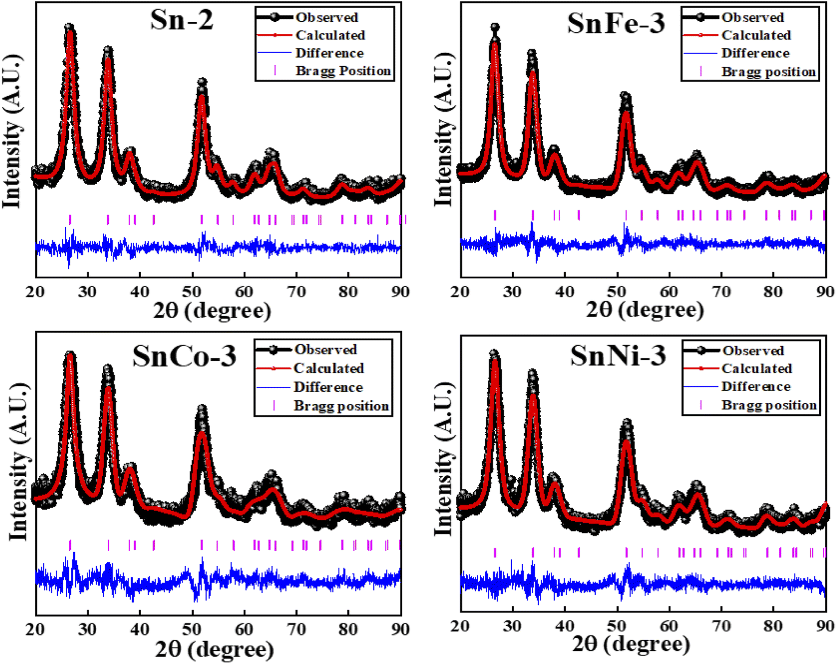 | ||
| Fig. 1 XRD patterns of pure and doped SnO2 nanocrystals. | ||
There was a slight change in the diffraction peak position and FWHM, giving rise to a slight change (increase/decrease) in the lattice parameters, which is due to the different cationic radii of Sn4+ (0.71 Å), Ni2+ (0.69 Å), Fe2+ (0.74 Å) and Co2+ (0.54 Å). The obtained crystallite size, lattice parameters and refined parameters of the SnCo-3, SnFe-3 and SnNi-3 samples are presented in the ESI (S Table 1).† Broadening of the (110) peak (FWHM) was observed for the Co- and Ni-doped samples, while the FWHM decreased for the Fe-doped sample, giving rise to a decrease and increase in the crystallite size of the corresponding samples, respectively, in comparison to the pure Sn-2 sample. The evolution of OV may affect the average size of the crystallite.36 With the aim to maintain the charge balance of the host lattice, some oxygen vacancies may have evolved due to the replacement of the lower oxidation state ions such as Co2+, Ni2+ and Fe2+.37 Thus, the slight shrinkage or expansion of the unit cell volume may have been related to the sizes of the substituted ions and the coordination effect related to the replacement of the Sn4+ ions by metal ions.
4.2 XPS analysis
To further understand the ionic states of the doped elements and to study the observed changes in the near surface chemical composition of the doped SnO2 samples, we performed XPS measurements. SnFe-3, SnCo-3 and SnNi-3 consist of well-recognized Sn 3d core level peaks, O 1s peaks and peaks of the doped (Fe, Co and Ni) elements. The wide XPS spectra of the doped SnO2 samples are shown in Fig. 2a, which confirm the presence of Co, Fe and Ni with the appearance of Co 2p, Fe 2p and Ni 2p peaks.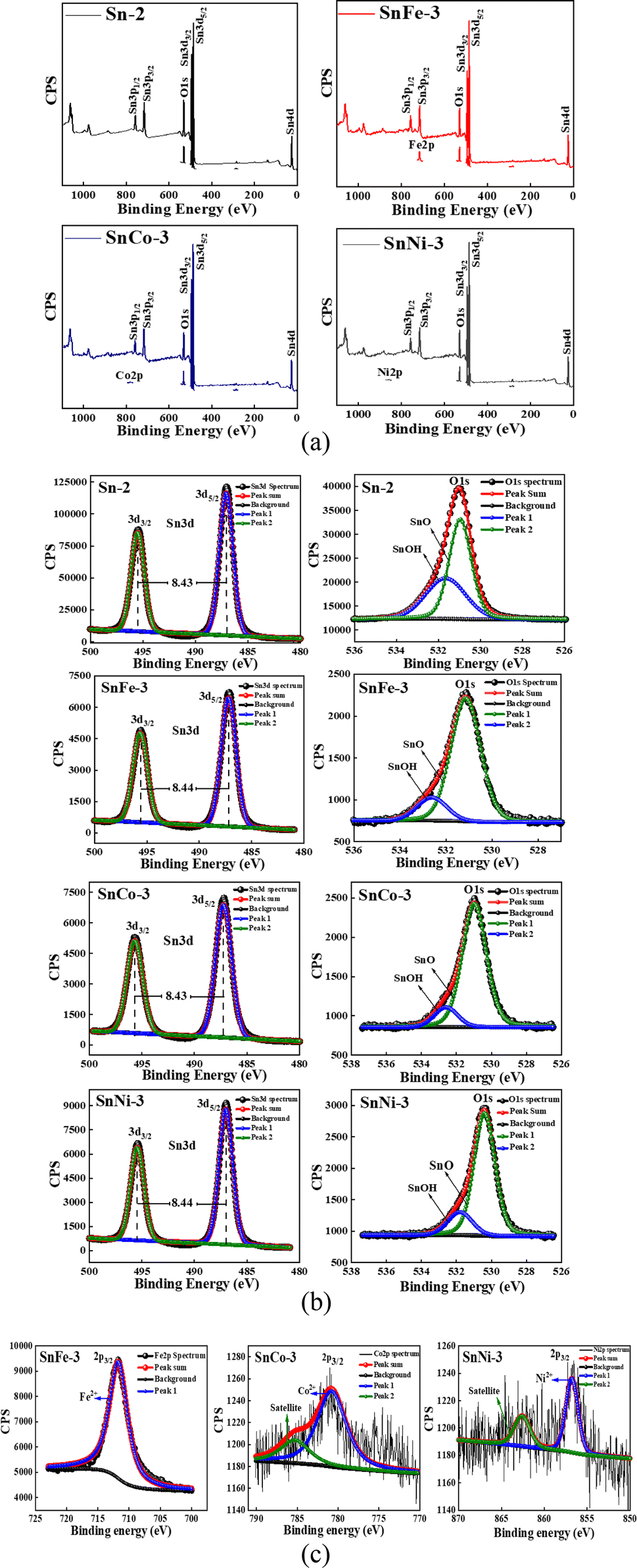 | ||
| Fig. 2 (a) Wide XPS spectra of pure and doped SnO2 samples. (b) High-resolution XPS spectra of pure and doped SnO2 samples corresponding to Sn 3d and O 1s orbitals. (c) High-resolution XPS spectra of doped SnO2 samples corresponding to the Fe 2p, Co 2p and Ni 2p orbitals. | ||
The Sn 3d energy levels and O 1s peaks of the parent and doped samples are shown in Fig. 2b. The Sn 3d spectra consist of a doublet located at 495.5 eV and 487.1 eV, which are ascribed to the BE of Sn 3d3/2 and Sn 3d5/2 respectively, with the peak separation (spin–orbit splitting) of around 8.4 eV. The obtained values are ascribed to the presence of Sn4+ ions in SnO2, which are in accordance with the earlier report.38 The high-resolution O 1s band was deconvoluted into two peaks located at 530.95 eV and 531.85 eV (Sn-2), 531.17 eV and 532.67 eV (SnFe-3), 531.03 eV and 532.67 eV (SnCo-3), 530.45 eV and 531.85 eV (SnNi-3), which may be due to the oxygen present in the lattice of SnO and hydroxyl group (–OH) oxygen.
It is interesting to note that the intensity of the Sn 3d and O 1s peaks was reduced in the doped SnO2 compared to the undoped sample. The reduction in the Sn 3d peak intensity can be ascribed to the substitution of Sn4+ ions with the doped ions. According to Fig. 2c, it is clear that all the doped ions carried a +2 charge, and thus we can conclude that two dopant ions may replace one parent Sn4+ ion. This replacement compensated the charge neutrality but still there was a shortage of Sn atoms which resulted in a reduction in the Sn 3d peak intensity. However, the highest Sn 3d peak reduction was observed for the SnFe-3 sample, indicating that the replacement of Sn4+ ions by Fe2+ ions is more in comparison to that of the Co and Ni dopants. Similarly, the reduction of the O 1s peak intensity in the doped SnO2 samples can be attributed to the OV created due to the defects caused by the dopants (Fe, Co, and Ni). Given that the highest replacement of Sn atoms was obtained for the SnFe-3 sample, the highest OV was also be seen for this sample because the O 1s peak intensity was reduced more compared to the other two doped samples. The deconvolution of the high-resolution O 1s spectra of all the samples is tabulated in the ESI (S Table 2)† and the corresponding (OV) quantification of the doped samples is presented in S Table 3† with respect to the O 1s spectrum of the parent SnO2. Moreover, it is interesting that more OV was created in all the doped samples give that there was a 10 times reduction in the peak intensity value of O 1s in comparison to the pure SnO2. However, the O 1s peak width was also observed to be increase with the doping of transition metal ions. This may be due to the difference in atoms at the surface or the adsorbed oxygen species such as hydroxyl groups or the oxygen deficiency created due to doping.
The high-resolution spectra of the dopants clearly show the presence of Fe 2p, Co 2p and Ni 2p, appearing at 711.52 eV, 780.66 eV and 856.53 eV, respectively, which are represented by the BE of 2p3/2, as shown in Fig. 2c. The deconvolution of the plots showed that all the dopants have one peak corresponding to the Fe2+, Co2+, and Ni2+ ions together with satellite peaks in SnCo-3 and SnNi-3. This indicates that the SnO2 structure was perturbed by the dopants by forming FeO, CoO and NiO structures, as shown in Fig. 2c, leading to a change in the properties of the parent SnO2. These values are in good well agreement with the previously reported work.39–41 All the XPS results obtained are consistent with the XRD studies.
4.3 TEM and HR-TEM analysis
The microstructure and morphology of the pure and doped SnO2 samples were studied through TEM, high-resolution TEM (HR-TEM) and SAED patterns. Fig. 3 (top lane) shows the TEM images of all the samples, in which spherical-shaped nanoparticles can be seen. The particle size was found to be in the range of 4–6 nm. Agglomeration of the particles was observed, which resulted in a variation in the particle size. The HR-TEM images in Fig. 3 (middle lane) clearly indicate the lattice fringes without any deformation in each sample, indicating the high purity of the nanocrystals. The calculated interplanar spacing of the neighboring lattice planes corresponds to the (110) plane of rutile SnO2, which are shown in the figures together with other planes (not shown), which are consistent with the XRD patterns (S Fig. 2a).† The inset in Fig. 4 (middle lane) shows the FFT patterns of the samples, further suggesting the crystalline nature and quality of the prepared samples. Fig. 3 (bottom lane) shows the SAED patterns of the samples, which indicate clear and distinct rings belonging to different planes of rutile SnO2 structures. The planes pertaining to different rings were identified by assessing the d-spacing value using the Image-J software, which are consistent with that from XRD, again in agreement with the HR-TEM images and lattice fringes obtained earlier.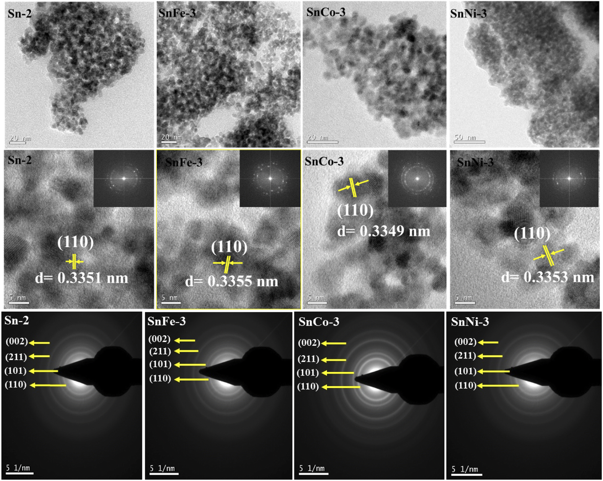 | ||
| Fig. 3 HRTEM data of pure and doped SnO2: (top lane) TEM images, (middle lane) HRTEM images with insets showing the FFT images and (bottom lane) SAED patterns. | ||
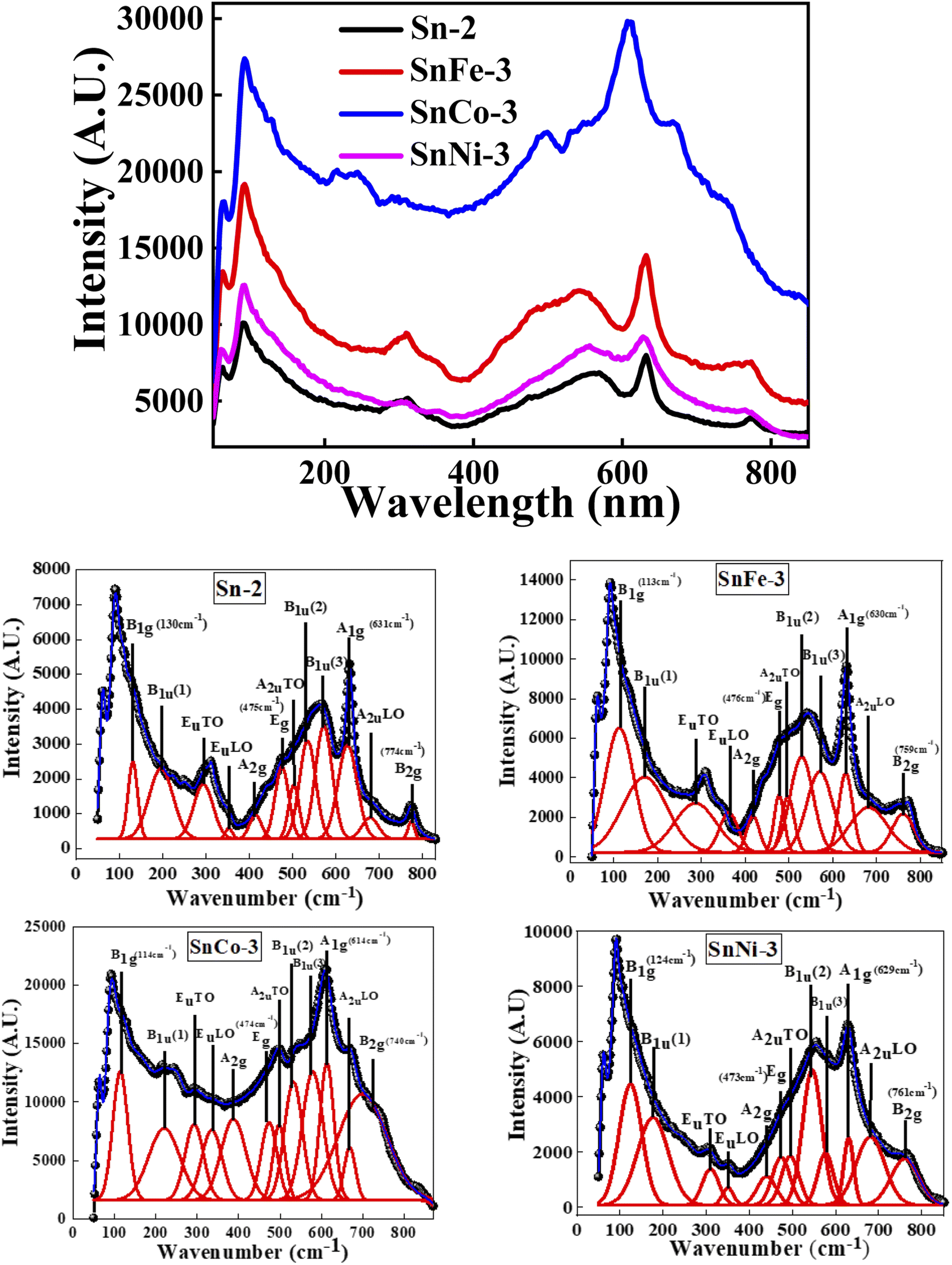 | ||
| Fig. 4 Raman spectra of pure and doped SnO2 nanocrystals in the top figure and the detailed fits are shown below for all the corresponding samples. | ||
4.4 Raman analysis
Raman spectroscopy was performed to determine the crystal structure, defects and disorder induced in the crystal because of the incorporation of the dopant in the host lattice. Fig. 4 (top) shows the micro-Raman spectra of all the samples and Fig. 4 (bottom) represents the corresponding plots of the individual samples together with the peak fitting using the Gaussian function taken at 300 K in the range of 0–800 cm−1. The optical exciton of the tetragonal rutile-type SnO2 crystal structure corresponds to the D4h point group. The irreducible representation of the D4h point group is A1g + A2g + A2u + B1g + B2g + 2B1u + Eg + 3Eu. Among them, the SnO2 crystal structure has four Raman-active modes (A1g, B1g, B2g and Eg), two IR-active vibrations (A2u, Eu) and two silent vibrations (A2g and B1u).42 The four active modes of single-crystal SnO2 are generally located at 130 (B1g), 475 (Eg), 631 (A1g) and 774 (B2g) cm−1,42,43 among which the A1g and Eg modes have a much higher intensity in comparison to B1g and B2g. The A1g, B1g and B2g vibrations belong to the expansion and contraction oscillation mode of the Sn–O bonds, while Eg corresponds to the vibrational motion of the oxygen atoms in the oxygen plane.44 The A1g, B1g and B2g modes oscillate perpendicular to the c-axis, whereas the Eg mode oscillates parallel to the c-axis. The Raman-active modes are due to the interior phonons, and thus are named the volume modes.45 The IR-active and silent vibrations are observed at 295 (EuTO), 354 (EuTO), 503 (AuTO), 680 (AuLO) and 197 (Bu(1)), 415 (A1g), 535 (Bu(2)), and 567 (Bu(3))cm−1, respectively. These additional modes besides the volume modes are due to the surface phonons, and thus are termed surface phonon modes.46 The feature at around 535 and 567 cm−1 is associated with the in-plane oxygen vacancies.47,48 Moreover, the surface properties of the nanocrystalline SnO2 are not only dependent on the crystallite size and distribution of the particles but also on the OV and disorder, which may result in the appearance of new modes in the Raman spectrum.49It can be observed that the most intense Raman band, i.e., A1g, together with the other peaks (B1g and B2g) shifted towards a lower wavenumber in the doped samples, where the shift in the peak orientation, intensity and FWHM is greater for the SnCO-3 sample. The A1g Raman mode is the highest mode of SnO2, which is associated with the vibration of the lattice oxygen atoms surrounding the Sn ions. Thus, the shift in this peak is peculiar to the change in O ions, and hence can be used as a measure of the existence of OV. The FWHM of this peak in all the doped samples was found to be higher in comparison to that of the parent SnO2 sample, giving an indication of the increase in OV in the doped samples. Thus, it is expected that the magnetic moment would be enhanced in the doped samples. The intensity and position of the peaks at 535 (Bu(2)) and 567 cm−1 (Bu(3)) also changed in the doped samples, indicating a large change in OV. Hence, all the results obtained clearly indicate that the dopants (Fe, Co and Ni) were finely incorporated in the host matrix.
4.5 FT-IR analysis
FT-IR spectroscopy was performed for the pure and doped SnO2 samples to examine the functional groups present in all the obtained product, as depicted in Fig. 5. All the spectra show the peaks in the range of 3300–3400 cm−1 (broad), 1625–1630 cm−1 and 1408 cm−1, corresponding to the O–H stretching and bending vibrations, which are ascribed to the adsorption of H2O molecules on the surface of SnO2.50 The broad peaks observed in the region of 670–550 cm−1 of the spectra for all the samples are attributed to the Sn–O–Sn stretching51 and Sn–O asymmetric stretching vibrations.52 However, in the present case, the value of the Sn–O–Sn stretching adsorption bands was found to be red-shifted for all the doped and undoped samples (i.e., stretching adsorption band is at 664 cm−1 for pure Sn-2 sample and at 655, 663 and 637 cm−1 for SnFe-3, SnCo-3 and SnNi-3, respectively). The change in the peak position of the SnO2 absorption bands suggests that the Sn–O–Sn network is perturbed with the presence of Co, Fe and Ni ions in its environment. Moreover, the shift in the peak position is much less, which may be due to the bond length differences that occur when the dopant ions replace the Sn ions. Therefore, the FT-IR results clearly confirm the incorporation of Co, Fe, and Ni ions in the SnO2 host matrix, as observed in the XRD, XPS and Raman measurements.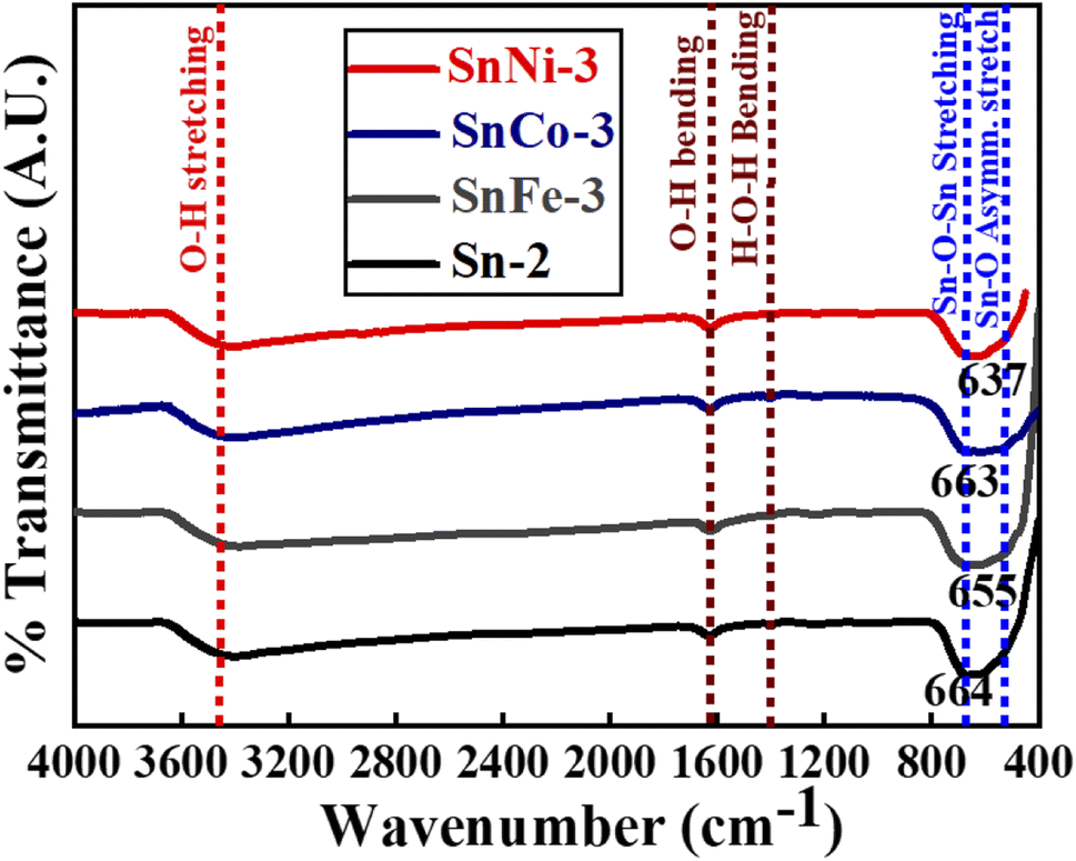 | ||
| Fig. 5 FT-IR spectra of pure and doped SnO2 nanocrystals. | ||
4.6 UV-vis spectroscopy analysis
To examine the influence of the dopants on the absorbance and optical bandgap of the parent nanocrystals, UV-visible absorbance spectra were measured for all the samples and the plots are given in Fig. 6a. The spectra show that in all the doped samples, the absorption peak position moved towards a higher wavelength or lower energies. It can also be noted that the Co-doped sample exhibited an additional peak between 385 and 475 nm, which can be related to the d–d electronic transition of Co2+ caused by crystal-field splitting in the six-coordination system (octahedral or pseudo-octahedral) and attributed to the 4T1g–4T1g(P) transition. Similar results have also been reported in ref. 53, where they noticed an equivalent peak in TiO2 nanoparticles doped with Co. The bandgap (Eg) of all the samples was determined using the Tauc plot, as showed in Fig. 6b. It was observed that the bandgap of SnFe-3, SnCo-3 and SnNi-3 decreased in comparison to SnO2. The reduction (red shift) in the bandgap of all the doped samples can be ascribed to the sp–d exchange interactions existing among the band (valence/conduction bands) electrons and the confined d electrons of the dopant ions (Co2+, Ni2+, and Fe2+) replacing the Sn4+ ions.54–56 Thus, the dopant played a key role in forming an impurity band in between the pure valence band and conduction band. Similarly, in ref. 57, a decrease in the bandgap of SnO2 doped with Fe3+ was reported due to the charge-transfer transition between the d-electrons of Fe3+ and conduction or valence band of SnO2. Similar work was also reported in ref. 58 and 59, where it was observed that the shift in the bandgap was due to the incorporation of cobalt and other transition metal ions. Hence, it is clear that the incorporation of dopant ions in the SnO2 crystal lattice is confirmed by the lowering of the bandgap.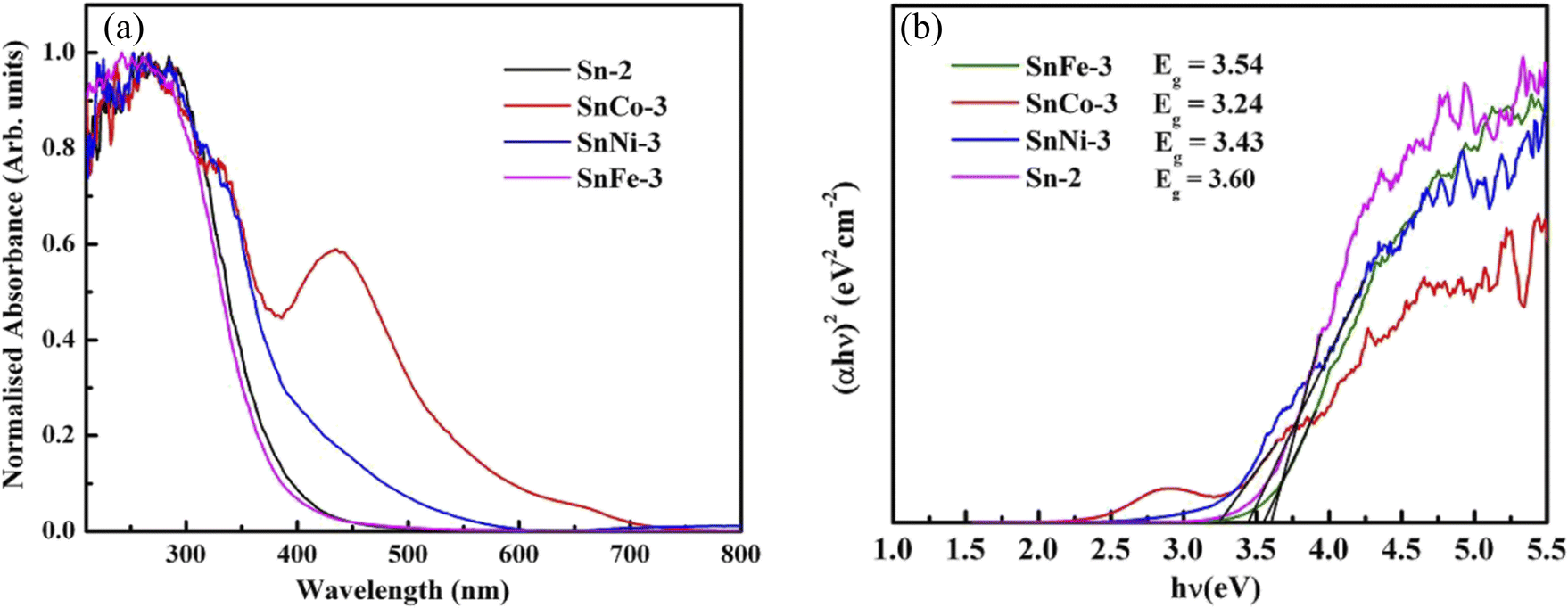 | ||
| Fig. 6 (a) UV-visible spectra of pure and doped SnO2 nanoparticles and (b) corresponding Tauc plots of the samples. | ||
4.7 PL spectroscopy analysis
PL spectroscopy was performed for all the samples at the excitation wavelength of 325 nm. PL is the most significant technique to determine the presence of impurities, excitons, surface defects, energy bands, etc. Fig. 7 shows the PL spectra and deconvoluted PL plots of the pure and doped SnO2 measured at room temperature. A broad feature was observed between 350 and 500 nm, which is attributed to the in-plane oxygen vacancies based on first principles calculations.60 When the broad peak was deconvoluted, it was seen to be composed of many peaks, where the peak at around 396 nm belongs to the electronic transition from the conduction band edge to the valence band edge, which can be due to the recombination of unbound excitons, i.e., electrons existing in the Sn 4p conduction band with their holes persisting in the O 2p valence band. The other emission band at around 420–480 nm corresponds to the blue emission, which may have arisen due to the generation of two-fold charged OV 61 It was observed from the spectra that Co, Ni, and Fe doping quenched the luminescence, due to which there was reduction in PL intensity. It was reported that Co ions act as luminescence quenchers for metal oxides such as TiO2 and ZnO, forming a large number of non-radiative recombination centres.62 Hence, here it can be inferred that Co, Ni, and Fe doping in the SnO2 nanocrystals increased the non-radiative recombination process.
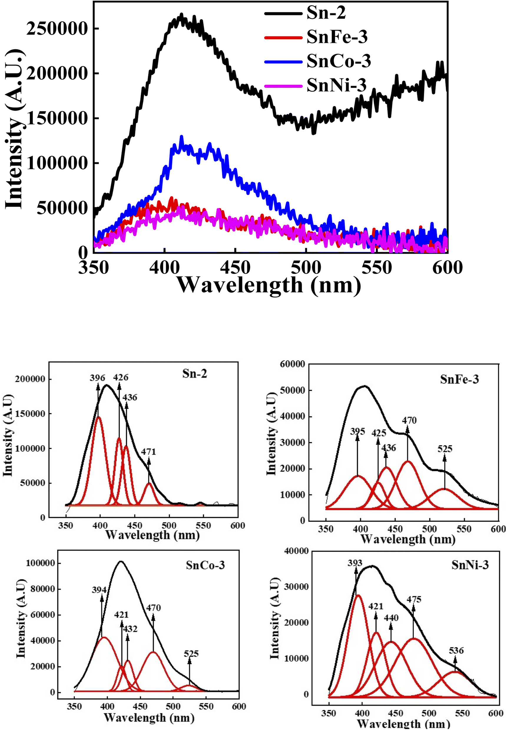 | ||
| Fig. 7 PL spectra of pure and doped SnO2 nanoparticles. | ||
4.8 Magnetic studies
The magnetic hysteresis loops of the pure and doped SnO2 samples were measured at 5 K and 300 K, as presented in Fig. 8. It was clearly observed that the pure SnO2 showed diamagnetism at both 5 K and 300 K, exhibiting a positive slope at the lower applied magnetic fields and a negative slope at a higher field of 5 K, whereas a negative slope at 300 K throughout the measured fields range. The diamagnetism in SnO2 is mainly due to the Sn ions existing in the +4 oxidation state (Sn4+), exhibiting a valence electronic configuration of [Kr] 5s2 4d10, which clearly shows that there is no unpaired electrons due to the existence of paramagnetism or ferromagnetism. However, when SnO2 was doped with Fe, Co and Ni, there was a clear change from diamagnetic behaviour to FM or PM behaviour at both 5 K and 300 K. The doped samples showed a positive slope at both 5 K and 300 K with a sharp increment in magnetisation at 5 K and a linear increment at 300 K. The results clearly show a good hysteresis loop with saturation magnetization at 5 K and lack of magnetic saturation at 300 K. The sharp increment in the magnetisation at 5 K with an increase in the applied field in the doped SnO2 may be due to the FM nature of the dopants. All the dopants, i.e., Fe, Co and Ni, are well-known FM elements due to the presence of unpaired electrons (domain ordering) in their valence shell, i.e., Fe2+ (d6), Co2+ (d7) and Ni2+ (d8), as confirmed by the XPS analysis. The sharp rise in the magnetisation up to the saturation point is due to the weakly coupled or uncoupled Fe2+, Co2+ and Ni2+ ions, suggesting the low-temperature magnetic ordering. Moreover, at low temperature (5 K, Fig. 9a), the thermal fluctuation of the domain (spin ordering) will be less, which allows the greater alignment of the spins in the ordered state with the applied field. The expanded version of the M–H loops at 5 K under low field (shown in Fig. 9c) shows that the coercivity of all the doped samples is almost the same at approximately 15 Oe, while the remanence of the SnFe-3, SnCo-3 and SnNi-3 samples is 0.014, 0.001 and 7.0 × 10⁻⁴ emu per g, respectively, which can be attributed to the weak FM or PM. In the case of the doped SnO2 samples at 300 K (Fig. 9b), the M–H loops are linear, with a linear increment in the magnetisation value with the applied field without any occurrence of magnetic saturation, suggesting PM or very weak FM behaviour. However, it is important to note that the M–H loops indicate very weak FM behavior at lower fields with almost zero coercivity and negligible remanence, as shown in Fig. 9d. Moreover, the very weak FM or PM at around 300 K can be attributed to the increase in the thermal fluctuation, resulting in the disturbance of domain ordering compared to FM behaviour at low temperature (5 K). Among the dopants, it can be seen that the magnetic moment of the Fe-doped sample is highest at 300 K and 5 K, which may be due to the greater amount of oxygen vacancies created in the sample, as inferred from the Raman spectra, as well as good alignment of the domains (spins) with the applied field given that there are less electrons in the valence shell (2 unpaired electrons), which will avoid repulsion for the correct alignment. However, in the case of SnCo-3 and SnNi-3, there are more electrons in their valence shell, which will interfere in the proper alignment of the domains with respect to the applied field due to repulsion.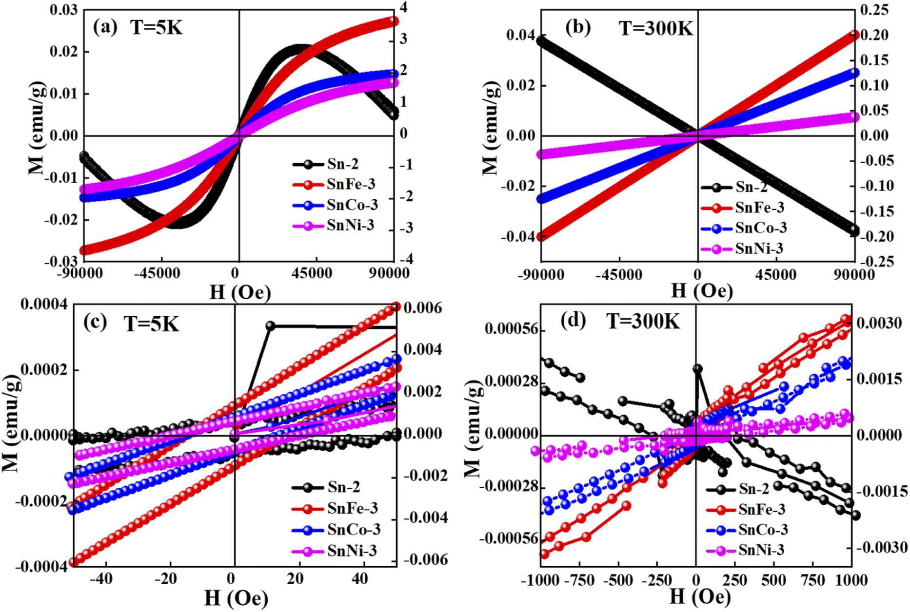 | ||
| Fig. 8 M–H curves of pure and doped SnO2 samples measured at (a) 5 K and (b) 300 K. (c) and (d) magnified view of (a) and (b), respectively, showing the hysteresis behavior. | ||
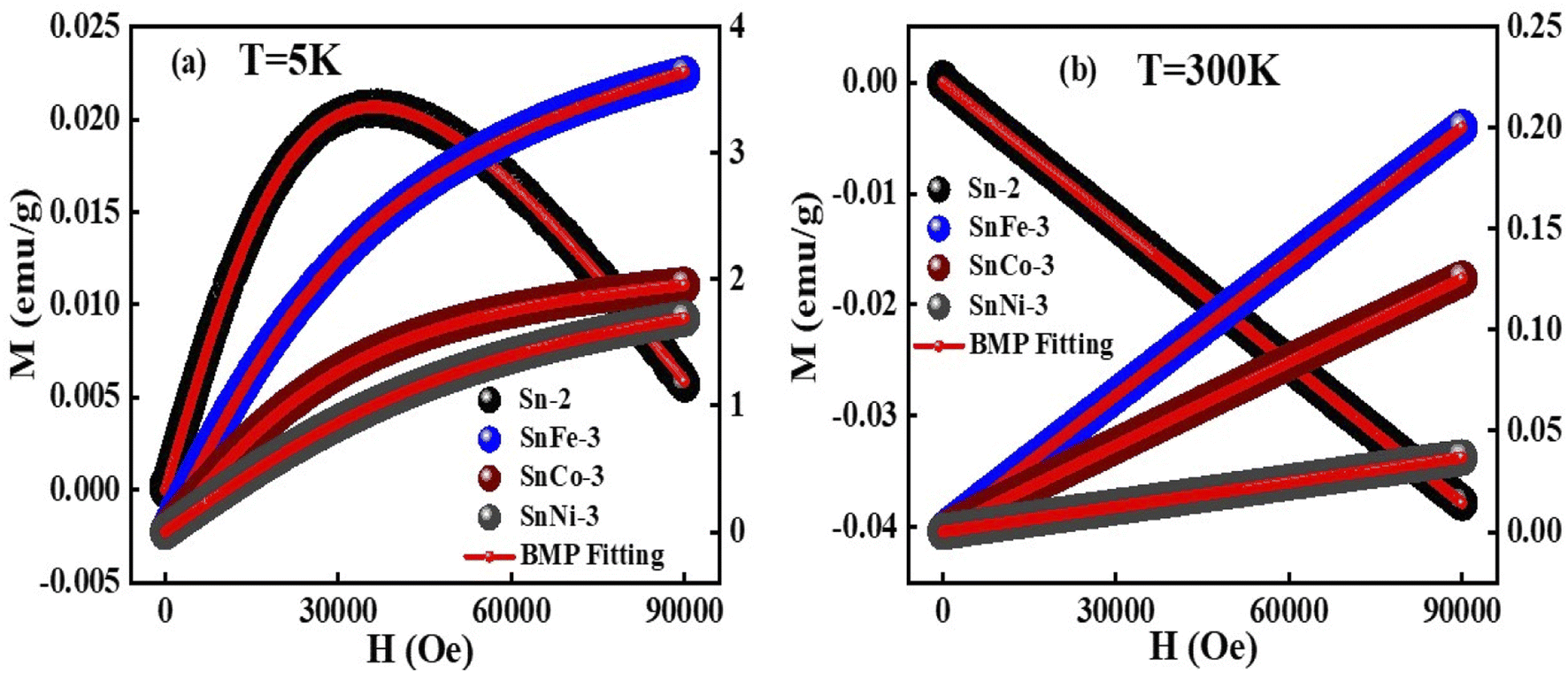 | ||
| Fig. 9 BMP-fitted M–H curves for SnFe-3, SnCo-3, SnNi-3 and SnO2 at (a) 5 K and (b) 300 K. Left axis represents the data related to the undoped sample (Sn-2), whereas the data on the right-axis belongs to the doped samples. | ||
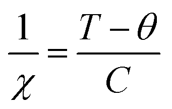
For a more in-depth understanding of the magnetic nature of the samples, the doped and undoped SnO2 samples were fitted with the bound magnetic polaron (BMP) model. The BMP model suggests that an electron gets trapped inside the vacant oxygen site or vacancy site and tries to interact with the applied field as well as neighbouring doped metal ions, constituting the BMP. BMP does not specify any electron, instead it is a combination of electrons and the surrounding strain field. Usually, a confined electron occupies an orbital that can overlap the d orbital of the doped metal ions. To study the FM nature, the BMP model was used given that its equation specifies both PM and FM natures. According to this model, the total magnetisation of the system is a combined effect of coordinated spins (i.e., overlapping of BMPs) and secluded spins. The corelated spin-induced magnetisation specifies FM and the magnetisation originating from the isolated spins specifies PM. Thus, the total magnetisation can be presented as Mtotal = MFM + MPM, where MPM can be given as χmH, χm is the PM susceptibility, H is the applied magnetic field and MFM can be given as M0L(x). M0 is the total spontaneous magnetic moment of the system, which is given by Nms, where ms corresponds to the definite spontaneous magnetic moment of all the BMP and N is the number of BMPs/volume. L(x) belongs to the Langevin function, which is given by [coth(x) − 1/x] where x = Hmeff/KBT, where meff is the productive spontaneous magnetic moment of all the BMP. Hence, Mtotal = M0L(x) + χmH.
The BMP model was used to fit the M–H curves, as presented in Fig. 9, and the BMP equation was fitted in the first quadrant of the hysteresis curve by taking M0, meff and χm as the variable parameters. It was clearly observed that the BMP model is exactly fits the M–H curves at 5 K for all the samples and the obtained variable parameters were tabulated in Table 1. At 5 K and 300 K, it was observed that the susceptibility of the undoped samples was negative, whereas that for the doped SnO2 samples was positive, which clearly suggests of diamagnetism and PM or FM, respectively. At 300 K, all the fitted curves are linear with respect to the doped samples, which clarifies the PM behavior in the doped samples. However, at a lower temperature, it seems that the number of BMPs is more, which governs the correlated spins, thus enhancing the magnetisation (FM) at low temperature compared to that at room temperature. Moreover, the saturation magnetisation obtained at 5 K was quite large at an applied field 9 T compared to that at 300 K, which did not reach saturation, and the increment in magnetisation was also small. The sharp increment and slightly higher values of saturation magnetisation at 5 K can be ascribed to the increase in the concentration of BMPs, which enhances the FM in the doped samples. Among the doped samples, SnFe-3 had the highest FM component at 5 K, which can be due to its greater number of BMPs. Moreover, the enhancement in magnetisation also depends on various factors such as the magnetic moment of the dopant, dopant concentration, and calcination conditions. However, the magnetisation of the doped SnO2 samples at 5 K cannot be purely FM, i.e., a mixture of PM and FM behavior, because the maximum saturation magnetisation obtained is 4 emu per g, which is significantly low to be FM. However, due to the contribution of the BMPs, sharp rise in magnetisation and uncoupled metal ions, a combination of PM and FM behaviours was observed.
| Sample | BMP fitted parameters | C–W fit parameters | ||||||
|---|---|---|---|---|---|---|---|---|
| N | At T = 5 K | At T = 300 K | C (emu per kOe per g) | TC (K) | ||||
| meff | χm | meff | χm | |||||
| Sn-2 | 1.02 × 10¹⁸ | 5.63 × 10⁻²⁰ | −4.86 × 10⁻⁷ ± 7.82 × 10⁻¹⁰ | 4.04 × 10⁻¹⁹ | −3.84 × 10⁻⁷ ± 2.06 × 10⁻⁷ | — | ||
| SnFe-3 | 7.45 × 10¹⁹ | 4.75 × 10⁻²⁰ | 7.51 × 10⁻⁶ ± 1.04 × 10⁻⁷ | 1.48 × 10⁻¹⁶ | 2.21 × 10⁻⁶ ± 1.55 × 10⁻¹⁰ | 7.4656 × 10⁻⁴ | −3.36274 ± 0.08338 | |
| SnCo-3 | 4.48 × 10¹⁹ | 4.93 × 10⁻²⁰ | 9.89 × 10⁻⁷ ± 1.58 × 10⁻⁸ | 3.23 × 10⁻¹⁷ | 1.38 × 10⁻⁶ ± 1.90 × 10⁻¹⁰ | 4.7804 × 10⁻⁴ | −4.13014 ± 0.0339 | |
| SnNi-3 | 6.06 × 10¹⁹ | 3.16 × 10⁻²⁰ | 2.66 × 10⁻⁶ ± 4.59 × 10⁻⁸ | 8.96 × 10⁻¹⁴ | 4.08 × 10⁻⁷ ± 9.48 × 10⁻¹¹ | 2.3492 × 10⁻⁴ | −1.97938 ± 0.03633 | |
Further details pertaining to the behavior of the magnetization phases with a decrease in temperature were analyzed using M vs. T measurements, which were taken in the field-cooled (FC) and zero field-cooled (ZFC) modes under a static magnetic field of 500 Oe. The FC–ZFC plots for all the samples overlapped, as shown in Fig. 10. Further, the magnetization values were observed to increase steadily with a decrease in temperature, followed by an abrupt increase at temperature below 100 K. It should be noted that in the case of pure SnO2 sample, negative magnetization was seen, which crossed to a positive value at a temperature around 25 K. This is because of the diamagnetic nature of the sample, where at lower temperatures, some of the spins get aligned due to the thermal fluctuation of the domains, thereby resulting in a positive magnetisation value. The Curie–Weiss (C–W) law was used to fit the M–T curves for all the samples and it was clearly observed that each doped-SnO2 sample was well-fitted from 300 K to 5 K, in contrast to the undoped SnO2 sample. This clearly suggests that SnO2 is diamagnetic and the doped samples are paramagnetic in nature.
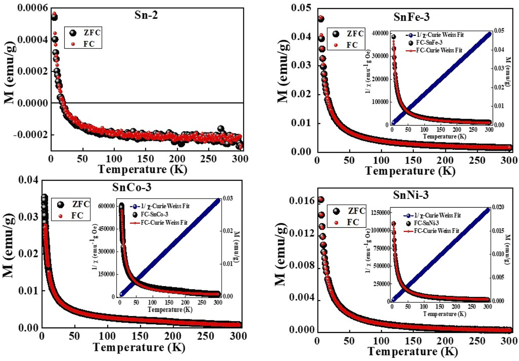 | ||
| Fig. 10 M–T curves of pure and doped SnO2 samples measured under a constant magnetic field of 500 Oe. | ||
5 Conclusion
The influence of Co, Fe and Ni dopants on the structural, optical and magnetic properties of SnO2 nanoparticles synthesized via a simple sol–gel method was studied. The XRD, Raman and TEM study indicated the formation of SnO2 without any secondary phases and confirmed the tetragonal rutile structure with P42/mnm space group. The clear lattice fringes seen in the high-resolution TEM images indicated the high crystallinity of the nanocrystals. The FWHM of the most intense Raman band, i.e., A1g, in all the doped samples, SnCo-3, SnFe-3 and SnNi-3, was found to be greater in comparison to that of the undoped SnO2 sample, giving indicating an increase in OV in all the doped compounds. The XPS analysis revealed the incorporation of divalent dopants (Fe2+, Co2+ and Ni2+) in the SnO2 host matrix together with the creation of OV. The UV-visible spectra indicate the lowering (redshift) of the bandgap in the doped samples, which is ascribed to the sp–d exchange interactions between the localized d electrons and the band electrons of the dopant ions (Co2+, Ni2+, and Fe2+), indicating the replacement of the Sn4+ ions by the dopant ions. The two emission peaks at around 395 nm are attributed to the electronic transition between the conduction band edge and valence band and the other at around 420–480 nm corresponds to the blue emission, which may have arisen due to the generation of two-fold charged OV as also noted from the photoluminescence spectra. The non-radiative recombination process increased due to Co, Ni and Fe doping in the SnO2 nanocrystals, as inferred from the PL study. The magnetic studies revealed the diamagnetic nature of pure SnO2 at room temperature and 5 K, whereas the coexistence of ferromagnetic and paramagnetic behavior in the doped SnO2 nanoparticles was observed, and the results were convincingly explained using the bound polaron model theory. Hence, the doped samples are a mix of FM and PM at 5 K and PM alone at 300 K. Thus, these materials have potential application in gas sensing, photocatalysis, and spin electronics.
Data availability
The authors confirm that the data supporting the findings of this study are available within the article.Author contributions
Supin K. K.: formal analysis, investigation, writing – rough draft. Anson George: synthesis, visualization, Y. Ranjith Kumar: partial analysis, Thejas: partial synthesis, Guruprasad Mandal: partial investigation. Anupama Chanda: writing – review and editing, M. Vasundhara: conceptualization, writing – review & editing, visualization, supervision, project administration, funding acquisition.Conflicts of interest
The authors declare that they have no known competing financial interests or personal relationships that could have appeared to influence the work reported in this paper. They also state that the manuscript is original and has not been published or not under consideration for publication elsewhere. All the authors are well aware of the content of the article and approved the submission.Acknowledgements
The authors would like to acknowledge the financial support received from Council of Scientific and Industrial Research (CSIR), Govt. of India. The authors would also like to thank the Department of Science and Technology sponsored project number CRG/2019/001574 for partially supporting this work. M. Vasundhara acknowledges the support offered by Department of K&IM (IICT/Pubs./2021/211).References
- G. A. Prinz, Science, 1998, 282, 1660–1663 CrossRef CAS PubMed.
- S. A. Wolf, D. D. Awschalom, R. A. Buhrman, J. M. Daughton, S. V. Molnar, M. L. Roukes, A. Y. Chtcheljanova and D. M. Treger, Science, 2001, 294, 1488–1495 CrossRef CAS PubMed.
- C. M. Wang, V. Shutthanandan, S. Thevuthasan, T. Droubay and S. A. Chambers, J. Appl. Phys., 2004, 95, 8185–8193 CrossRef CAS.
- K. C. Verma and R. K. Kotnala, J. Solid State Chem., 2017, 246, 150–159 CrossRef CAS.
- Y. Zhang, A. Kolmakov, S. Chretien, H. Metiu and M. Moskovits, Nano Lett., 2004, 4, 403–407 CrossRef CAS.
- Y. Wang, H. C. Zeng and J. Y. Lee, Adv. Mater., 2006, 18, 645–649 CrossRef CAS.
- Y. Wang, J. Y. Lee and H. C. Zeng, Chem. Mater., 2005, 17, 3899–3903 CrossRef CAS.
- D. Chu, Y. Masuda, T. Ohji and K. Kato, Chem. Eng. J., 2011, 168, 955–958 CrossRef CAS.
- A. Aslani, V. Oroojpour and M. Fallahi, Appl. Surf. Sci., 2011, 257, 4056–4061 CrossRef CAS.
- Y. Matsumoto, M. Murakami, T. Shono, T. Hasegawa, T. Fukumura, M. Kawasaki, P. Ahmet, T. Chikyow, S. Koshihara and H. Koinuma, Science, 2011, 291, 854–856 CrossRef.
- S. B. Ogale, R. J. Choudhary, J. P. Buban, S. E. Lofland, S. R. Shinde, S. N. Kale, V. N. Kulkarni, J. Higgins, C. Lanci, J. R. Simpson, N. D. Browning, S. Das Sarma, H. D. Drew, R. L. Greene and T. Venkatesan, Phys. Rev. Lett., 2003, 91, 077205 CrossRef CAS PubMed.
- C. B. Fitzgerald, M. Venkatesan, A. P. Douvalis, S. Huber, J. M. D Coey and T. Bakas, J. Appl. Phys., 2004, 95, 7390–7392 CrossRef CAS.
- A. Punnoose, J. Hays, V. Gopal and V. Shutthanandan, Appl. Phys. Lett., 2004, 85, 1559–1561 CrossRef CAS.
- A. Punnoose, J. Hays, A. Thurber, M. H. Engelhard, R. K. Kukkadapu, C. Wang, V. Shutthanandan and S. Thevuthasan, Phys. Rev. B: Condens. Matter Mater. Phys., 2005, 72, 054402 CrossRef.
- J. Hays, A. Punnoose, R. Baldner, M. H. Engelhard, J. Peloquin and K. M. Reddy, Phys. Rev. B: Condens. Matter Mater. Phys., 2005, 72, 075203 CrossRef.
- J. M. D. Coey, A. P. Douvalis, C. B. Fitzgerald and M. Venkatesan, Appl. Phys. Lett., 2004, 84, 1332–1334 CrossRef CAS.
- H. Kimura, T. Fukumura, M. Kawasaki, K. Inaba, T. Hasegawa and H. Koinuma, Appl. Phys. Lett., 2002, 80, 94–96 CrossRef CAS.
- A. Sharma, M. Varshney, S. Kumar, K. D. Verma and R. Kumar, Nanomater. Nanotechnol., 2011, 1, 6 CrossRef.
- R. Adhikari, A. K. Das, D. Karmakar, T. V. C. Rao and J. Ghatak, Phys. Rev. B: Condens. Matter Mater. Phys., 2008, 78, 024404 CrossRef.
- N. H. Hong, J. Sakai, N. T. Huong, N. Poirot and A. Ruyter, Phys. Rev. B: Condens. Matter Mater. Phys., 2005, 72, 045336 CrossRef.
- N. H. Hong, A. Ruyter, W. Prellier, J. Sakai and N. T. Huong, J. Phys.: Condens. Matter, 2005, 17, 6533 CrossRef CAS.
- L. S. Chuah, M. S. Yaacob and Z. Hassan, Optoelectron. Adv. Mater., Rapid Commun., 2012, 6, 149–153 CAS.
- Y. Chen, L. Yu, D. Feng, M. Zhuo, M. Zhang, E. Zhang, Z. Xu, Q. Li and T. Wang, Sens. Actuators, B, 2012, 166, 61–67 CrossRef.
- M. Dehbashi and M. A. Ahmad, Int. J. Phys. Sci., 2012, 7, 5415–5420 CAS.
- M. A. Ahmad and M. Dehbashi, Iran. J. Energy Environ., 2013, 4, 49–52 Search PubMed.
- A. Sharma, M. Varshney, S. Kumar, K. D. Verma and R. Kumar, Nanomater. Nanotechnol., 2011, 1, 6 CrossRef.
- F. H. Aragon, J. A. H. Coaquira, P. Hidalgo, S. W. Da Silva, S. L. Brito, D. Gouvêa and P. C. Morais, J. Raman Spectrosc., 2011, 42, 1081–1086 CrossRef CAS.
- Q. Ru, Appl. Phys. Lett., 1997, 71, 1792–1794 CrossRef CAS.
- S. Music, S. Popovic, M. Metikos-Hukovic and V. Gvozdic, J. Mater. Sci. Lett., 1991, 10, 197–200 CrossRef CAS.
- M. Kuppan, S. Kaleemulla, N. M. Rao, N. S. Krishna, M. R. Begam and D. S. Reddy, J. Supercond. Novel Magn., 2014, 27, 1315–1321 CrossRef CAS.
- G. Ramanathan and K. R. Murali, J. Appl. Electrochem., 2022, 52, 849–859 CrossRef CAS.
- B. P. Narasaiah, P. Banoth, A. Sohan, B. K. Mandal, A. G. B. Dominguez, L. De Los Santos Valladares and P. Kollu, ACS Omega, 2022, 7, 15423–15438 CrossRef CAS PubMed.
- P. Wu, S. Wang, X. Li, F. Zhang and F., J. Mater. Chem. A, 2021, 9, 19554–19588 RSC.
- Y. Masuda, Sens. Actuators, B, 2022, 364, 131876 CrossRef CAS.
- S. U. Din, S. H. Kiani, S. Haq, P. Ahmad, M. U. Khandaker, M. R. I. Faruque, A. M. Idris and M. I. Sayyed, Crystals, 2022, 12, 614 CrossRef CAS.
- N. Ahmad and S. Khan, J. Alloys Compd., 2017, 720, 502–509 CrossRef CAS.
- F. H. Aragon, J. A. H. Coaquira, I. Gonzalez, L. C. C. M. Nagamine, W. A. A. Macedo and P. C. Morais, J. Phys. D: Appl. Phys., 2016, 49, 155002 CrossRef.
- H. Cai, H. Liu, T. Ni, Y. Pan, Y. Zhao and Y. Zhu, Front. Chem., 2019, 7, 843 CrossRef CAS PubMed.
- J. Hu, Y. Wang, W. Wang, Y. Xue, P. Li, K. Lian, L. Chen, W. Zhang and S. Zhuiykov, J. Mater. Sci., 2017, 52, 11554–11568 CrossRef CAS.
- S. Malvankar, S. Doke, R. Gahlaut, E. Martinez-Teran, A. A. El-Gendy, U. Deshpande and S. Mahamuni, J. Electron. Mater., 2020, 49, 1872–1880 CrossRef CAS.
- S. Singkammo, A. Wisitsoraat, C. Sriprachuabwong, A. Tuantranont, S. Phanichphant and C. Liewhiran, ACS Appl. Mater. Interfaces, 2015, 7, 3077–3092 CrossRef CAS PubMed.
- P. S. Peercy and B. Morosin, Phys. Rev. B: Solid State, 1973, 7, 2779–2786 CrossRef CAS.
- D. Dutta and D. Bahadur, J. Mater. Chem., 2012, 22, 24545–24551 RSC.
- K. N. Yu, Y. Xiong, Y. Liu and C. Xiong, Phys. Rev. B: Condens. Matter Mater. Phys., 1997, 55, 2666–2671 CrossRef CAS.
- L. Abello, B. Bochu, A. Gaskov, S. Koudryavtseva, G. Lucazeauand and M. Roumyantseva, J. Solid State Chem., 1998, 135, 78–85 CrossRef CAS.
- J. X. Wang, D. F. Liu, X. Q. Yan, H. J. Yuan, L. J. Ci, Z. P. Zhou, Y. Gao, L. Song, L. F. Liu, W. Y. Zhou, G. Wang and S. S. Xie, Solid State Commun., 2004, 130, 89–94 CrossRef CAS.
- A. Kar, S. Kundu and A. Patra, J. Phys. Chem. C, 2011, 115, 118–124 CrossRef CAS.
- L. Z. Liu, J. Q. Xu, X. L. Wu, T. H. Li, J. C. Shen and P. K. Chu, Appl. Phys. Lett., 2013, 102, 031916 CrossRef.
- J. Kaur, J. Shah, R. K. Kotnala and K. C. Verma, Ceram. Int., 2012, 38, 5563–5570 CrossRef CAS.
- M. Faisal, A. A. Ibrahim, F. A. Harraz, H. Bouzid, M. S. Al-Assiri and A. A. Ismail, J. Mol. Catal. A: Chem., 2015, 397, 19–25 CrossRef CAS.
- S. Gnanam and V. Rajendran, J. Sol-Gel Sci. Technol., 2010, 56, 128–133 CrossRef CAS.
- S. H. Mohamed, J. Alloys Compd., 2012, 510, 119–124 CrossRef CAS.
- B. Choudhury and A. Choudhury, J. Lumin., 2012, 132, 178–184 CrossRef CAS.
- T. Entradas, J. F. Cabrita, S. Dalui, M. R. Nunes, O. C. Monteiro and A. J. Silvestre, Mater. Chem. Phys., 2014, 147, 563–571 CrossRef CAS.
- M. K. Lima, D. M. Fernandes, M. F. Silva, M. L. Baesso, A. M. Neto, G. R. Morais, C. V. Nakamura, A. O. Caleare, A. A. W. Hechenleitner and E. A. G. Pineda, J. Sol-Gel Sci. Technol., 2014, 72, 301–309 CrossRef CAS.
- D. H. Kim, H. S. Hong, S. J. Kim, J. S. Song and K. S. Lee, J. Alloys Compd., 2004, 375, 259–264 CrossRef CAS.
- L. M. Fang, X. T. Zu, Z. J. Li, S. Zhu, C. M. Liu, W. L. Zhou and L. M. Wang, J. Alloys Compd., 2008, 454, 261–267 CrossRef CAS.
- B. Santara, B. Pal and P. K. Giri, J. Appl. Phys., 2011, 110, 114322 CrossRef.
- B. Choudhury, M. Dey and A. Choudhury, Int. Nano Lett., 2013, 3, 1–8 CrossRef CAS.
- L. Z. Liu, J. Q. Xu, X. L. Wu, T. H. Li, J. C. Shen and P. K. Chu, Appl. Phys. Lett., 2013, 102, 031916 CrossRef.
- P. Chetri, B. Saikia and A. Choudhury, J. Appl. Phys., 2013, 113, 233514 CrossRef.
- S. Yamamot, J. Appl. Phys., 2012, 111, 094310 CrossRef.
- V. R. Akshay, B. Arun, G. Mandal and M. Vasundhara, New J. Chem., 2019, 43, 14786–14799 RSC.
- V. R. Akshay, B. Arun, G. Mandal and M. Vasundhara, Phys. Chem. Chem. Phys., 2019, 21, 12991–13004 RSC.
- V. R. Akshay, B. Arun, G. Mandal, G. R. Mutta, A. Chanda and M. Vasundhara, New J. Chem., 2019, 43, 6048–6062 RSC.
- V. R. Akshay, B. Arun, G. Mandal and M. Vasundhara, Phys. Chem. Chem. Phys., 2019, 21, 2519–2532 RSC.
- V. R. Akshay, B. Arun, S. Dash, A. K. Patra, G. Mandal, G. R. Mutta, A. Chanda and M. Vasundhara, RSC Adv., 2018, 8, 41994–42008 RSC.
- V. R. Akshay, B. Arun, G. Mandal, G. R. Mutta, A. Chanda and M. Vasundhara, J. Phys. Chem. C, 2018, 122, 26592–26604 CrossRef CAS.
- F. H. Aragan, J. A. H. Coaquira, P. Hidalgo, S. L. M Brito, D. Gouvea and R. H. R. Castro, J. Phys.: Condens. Matter, 2010, 22, 496003 CrossRef PubMed.
Footnote |
| † Electronic supplementary information (ESI) available. See https://doi.org/10.1039/d2ra03691f |
| This journal is © The Royal Society of Chemistry 2022 |