
 Open Access Article
 This Open Access Article is licensed under a Creative Commons Attribution-Non Commercial 3.0 Unported Licence
Strain coupling of ferroelastic domains and misfit dislocations in [101]-oriented ferroelectric PbTiO3 films
Y. P. Fengab,
R. J. Jiangcd,
Y. L. Zhu *a,
Y. L. Tangc,
Y. J. Wangc,
M. J. Zouab,
W. R. Gengab and
X. L. Maabe
*a,
Y. L. Tangc,
Y. J. Wangc,
M. J. Zouab,
W. R. Gengab and
X. L. Maabe
aBay Area Center for Electron Microscopy, Songshan Lake Materials Laboratory, Dongguan, Guangdong 523808, China. E-mail: zhuyinlian@sslab.org.cn
bInstitute of Physics, Chinese Academy of Sciences, Beijing 100190, China
cShenyang National Laboratory for Materials Science, Institute of Metal Research, Chinese Academy of Sciences, Wenhua Road 72, Shenyang 110016, China
dSchool of Materials Science and Engineering, University of Science and Technology of China, Wenhua Road 72, Shenyang 110016, China
eState Key Lab of Advanced Processing and Recycling on Non-ferrous Metals, Lanzhou University of Technology, Langongping Road 287, Lanzhou 730050, China
First published on 14th July 2022
Abstract
High-index perovskite ferroelectric thin films possess excellent dielectric permittivity, piezoelectric coefficient, and exotic ferroelectric switching properties. They also exhibit complications in the ferroelastic domains, misfit dislocations, and strain-relaxation behaviors. Exploring the relationship of the ferroelastic domains and misfit dislocations may be of benefit for promoting the high-quality growth of these thin films. Here, the strain field of the ferroelastic domains and misfit dislocations in [101]-oriented PbTiO3/(La, Sr)(Al, Ta)O3 epitaxial thin films were investigated by advanced aberration-corrected (scanning) transmission electron microscopy (TEM) combined with geometry phase analysis (GPA). Two types of misfit dislocations with projected Burgers vectors of a[001] or a[100] on the (010) plane were elucidated, whose strain fields included in-plane strain and lattice rotation coupled with the c domains above them. Besides, it was demonstrated that the coupling was kept inside the PbTiO3 films when the film thickness was increased. Furthermore, the polarization rotation was observed in both narrow c domains and around the misfit dislocation cores, which may be attributed to the flexoelectric effect. These results are expected to provide useful information for understanding the nucleation and propagation mechanism of ferroelastic domains and for further modifying the growth of high-index ferroelectric thin films.
1. Introduction
Perovskite ferroelectric oxide thin films have large potential for application in next-generation memory devices, advanced electromechanical devices, and field effect transistors due to their remarkable electromechanical responses and nonvolatile ferroelectricity.1–3 Strain engineering has been used to modify their electric properties with the careful selection of substrate materials.4,5 In general, lattice mismatch is inevitable when ferroelectric oxide thin films are grown on various substrates. However, once the lattice mismatch exceeds a critical value or the ferroelectric oxide thin film is up to a critical thickness, misfit dislocations are generated.6In the past decades, the effects of such dislocations on the physical properties were extensively researched. On the one hand, the misfit dislocations can reduce ferroelectric polarization and the piezoelectric responses. Chu et al. observed the polarization instability and a deterioration of the piezoelectric responses in Pb(Zr0.52Ti0.48)O3 nanoislands.7 Alpay et al. reported that the misfit dislocations can degrade the ferroelectricity in a region about several nanometers around the dislocation cores due to the depolarizing field induced by the coupling of the stress field of the dislocation and polarization.8 In particular, Jia et al. reported that a single dislocation can decrease the local spontaneous polarization by up to 48%.9 However, many researchers have reported contradictory results. For instance, the coercive field was reduced and meanwhile the remanent polarization was enhanced by introducing a proper density of dislocations in ferroelectric single-crystals.10 A giant strain gradient appeared and consequently the visible-light-absorption property was enhanced by introduced periodic misfit dislocations in BiFeO3/LaAlO3(001) nanostructures via high-flux deposition.11 Besides, the introduction of dislocation networks by a mechanically imprinting method in ferroelectric BaTiO3 single-crystals could largely enhance the dielectric and electromechanical responses, while the paraelectric SrTiO3 single-crystal exhibited enhanced superconductivity and ferroelectric quantum criticality by the modification of the self-organized dislocations.12,13
For ferroelectric PbTiO3 (PTO) thin films, the formation of a 180°/90° multidomain configuration could reduce the total energy of the system, which depended on the elastic strain energy, electrostatic energy, and domain wall energy.14 While the 180° domain wall with a slight wall thickness only showed lattice rotation, the 90° a/c domain walls with a non-negligible width possessed a considerable ferroelastic strain field, including lattice rotation and a lattice difference across the a/c domain walls.15–17 The introduction of misfit dislocations or dislocation networks in ferroelectric films will change the local strain field, which interacts with the strain field of ferroelastic domains and consequently results in changes in the polarization distribution and domain walls pinning.18,19 The elastic interaction between misfit dislocations and the domain walls was reported in [001]-oriented Pb(Zr0.4Ti0.6)O3 islands and PbTiO3/SrTiO3(001) epitaxial thin films.20,21 Recently, high-index-oriented ferroelectric thin films have been widely investigated due to their excellent dielectric, piezoelectric responses and exotic ferroelectric switching.22–24 Furthermore, the domain configurations, misfit dislocations, and strain-relaxation behaviors in [101]- and [111]-oriented ferroelectric films revealed significant differences compared with those in [001]-oriented ferroelectric films,25–29 which certainly complicates the relationship of the strain fields between ferroelastic domains and misfit dislocations. A giant strain gradient might be induced around dislocation cores, which can modify the ferroelectric polarization in high-index ferroelectric thin films.30
In this study, we investigated the strain field of ferroelastic 90° domains and misfit dislocations in [101]-oriented ferroelectric PTO thin films grown on the (La, Sr)(Al, Ta)O3 (LSAT) substrates by advanced aberration-corrected high-angle annular dark-field (HAADF) scanning transmission electron microcopy (STEM). We not only elucidated the strain field coupling of ferroelastic 90° domains and misfit dislocations but also demonstrated the changes in polarization distribution around dislocation cores.
2. Experimental
Film deposition
The PTO films were deposited on single-crystal [101]-oriented LSAT (LSAT(101)) substrates by pulsed laser deposition (PLD) with the wavelength of a Coherent ComPex PRO 201KrF excimer laser at a wavelength of λ = 248 nm. The sintered PTO target with 3 mol% Pb-enriched was used for the film deposition. The target–substrate distance was adjusted to 80 mm. Before PTO film deposition, the LSAT substrates were heated to 800 °C for 10 min and the PTO target was also pre-sputtered for 5 min to clean the substrate and target surfaces, respectively. During deposition, a deposition temperature of 700 °C, oxygen pressure of 10 Pa, laser energy density of 2 J cm−2, and repetition rate of 4 Hz were used. After deposition, the PTO films were kept at 700 °C for 5 min in an oxygen pressure of 3 × 10⁴ Pa, and then cooled down to room temperature at the cooling rate of 5 °C min−1.X-ray diffraction analysis
X-ray diffraction (XRD) with the 2θ range of 20°–80° was used to test the crystalline quality of the PTO films grown on [101]-oriented LSAT substrates using a Bruker D8 Advance X-ray diffractometer.TEM sample preparation
Cross-sectional TEM samples were prepared by a conventional method of gluing, grinding, dimpling, and ion milling. Before ion milling, the samples were dimpled down to about 10 μm. A precision ion polishing system (PIPS) 691 (Gatan Company, USA) was used for the final ion milling. Plane-view TEM samples were ground, dimpled, and ion milled only from the substrate side. During ion milling, a voltage of 5 kV and incident angle of 7° were used at first. Then, the angle was gradually reduced to 4.5°. For final ion milling, the voltage of 0.5 kV and the incident angle of 4.5° for 5–10 min were used to reduce the surface damage by the ion beam.TEM observation, HAADF-STEM imaging, strain field analysis, and determination of the position of the atom columns
Bright- and dark-field TEM images were acquired using a Tecnai F30 transmission electron microscope. Selected area electron diffraction (SAED) patterns were acquired using a JEM 2100 (JEOL, Japan) transmission electron microscope. All the cross-sectional HAADF-STEM images were acquired with a beam convergence angle of 25 mrad and collection angle of 50–250 mrad using a Titan G2 60–300 aberration-corrected scanning transmission electron microscope (ThemoFisher Scientific Company, USA) at 300 kV. The large-scale strain fields were extracted using geometry phase analysis (GPA), carried out by using Gatan Digital Micrograph software. The positions of the Pb and Ti atom columns in the HAADF-STEM images were determined accurately based on two-dimensional (2D) Gaussian fitting, which was performed in Matlab software.31–333. Results
At room temperature, the PTO crystal exhibited a tetragonal structure (P4mm) with the lattice parameters of a = b = 0.390 nm and c = 0.415 nm, and the LSAT crystal was a typical cubic structure (Pm![[3 with combining macron]](https://www.rsc.org/images/entities/char_0033_0304.gif) m) with lattice parameters of a = b = c = 0.3868 nm.34,35 Fig. 1 shows a typical XRD θ–2θ scan pattern of the PTO/LSAT(101) thin film. The two strong peaks were Kα peaks and were indexed to the (101) and (202) of LSAT, respectively. In general, the Kα radiation of the Cu target contains Kα1 and Kα2, which resulted in a split of the strong Kα peaks of LSAT. The weak peaks near the strong peaks labeled by red arrows were from the (101) and (202) of PTO, respectively. The blue arrows denote the Kβ peaks of (101) and (202) of LSAT. It could be seen that the PTO films exhibited good crystallinity with a single perovskite structure and no impurity phases could be identified. Fig. 2(a) is a cross-sectional bright-field TEM image of the PTO/LSAT(101) films. The film thickness was about 50 nm. A pair of opposite arrows denote the PTO/LSAT interface. Vertical stripe domains with bright and dark contrasts can be seen clearly in the PTO films. Besides, a little inclined domain labeled with a red arrow in Fig. 2(a) appeared in the PTO films. As reported previously, these domains were ferroelastic 90° c1/c2 and a/c domains, respectively.25 It may be noted that some dot-like defects could be seen at the PTO/LSAT interface. Fig. 2(b) presents a two-beam dark-field TEM image taken by the diffraction vector of g =
m) with lattice parameters of a = b = c = 0.3868 nm.34,35 Fig. 1 shows a typical XRD θ–2θ scan pattern of the PTO/LSAT(101) thin film. The two strong peaks were Kα peaks and were indexed to the (101) and (202) of LSAT, respectively. In general, the Kα radiation of the Cu target contains Kα1 and Kα2, which resulted in a split of the strong Kα peaks of LSAT. The weak peaks near the strong peaks labeled by red arrows were from the (101) and (202) of PTO, respectively. The blue arrows denote the Kβ peaks of (101) and (202) of LSAT. It could be seen that the PTO films exhibited good crystallinity with a single perovskite structure and no impurity phases could be identified. Fig. 2(a) is a cross-sectional bright-field TEM image of the PTO/LSAT(101) films. The film thickness was about 50 nm. A pair of opposite arrows denote the PTO/LSAT interface. Vertical stripe domains with bright and dark contrasts can be seen clearly in the PTO films. Besides, a little inclined domain labeled with a red arrow in Fig. 2(a) appeared in the PTO films. As reported previously, these domains were ferroelastic 90° c1/c2 and a/c domains, respectively.25 It may be noted that some dot-like defects could be seen at the PTO/LSAT interface. Fig. 2(b) presents a two-beam dark-field TEM image taken by the diffraction vector of g = ![[1 with combining macron]](https://www.rsc.org/images/entities/char_0031_0304.gif) 01c, where the subscript “c” denotes the cubic LSAT substrate. At this diffraction vector of g = 01c, the vertical stripe domains disappeared, which allows the dot-like defects (labeled as blue arrows) to be easily seen, as shown in Fig. 2(b). Fig. 2(c) is a selected area electron diffraction (SAED) pattern for the area including the PTO film and LSAT substrate taken along the [010] zone axis of a 50 nm PTO film. The inset is a magnified area showing the out-of-plane (101) spots corresponding to the white rectangle box in Fig. 2(c). Since d110 = 0.276 nm, d101 = 0.284 nm of PTO, and d110 = d101 = 0.274 nm of LSAT, the (101) spots could be easily identified, as shown in the inset of Fig. 2(c). To present the relationship between the stripe domains and interfacial misfit dislocation, plane-view TEM imaging was further performed. In Fig. 2(d), it can be seen that the stripe domains exhibited an alternate bright and dark arrangement, which evolved along the in-plane [010] direction. However, the misfit dislocations were along the in-plane [1] and [11] directions, as shown in Fig. 2(e).
01c, where the subscript “c” denotes the cubic LSAT substrate. At this diffraction vector of g = 01c, the vertical stripe domains disappeared, which allows the dot-like defects (labeled as blue arrows) to be easily seen, as shown in Fig. 2(b). Fig. 2(c) is a selected area electron diffraction (SAED) pattern for the area including the PTO film and LSAT substrate taken along the [010] zone axis of a 50 nm PTO film. The inset is a magnified area showing the out-of-plane (101) spots corresponding to the white rectangle box in Fig. 2(c). Since d110 = 0.276 nm, d101 = 0.284 nm of PTO, and d110 = d101 = 0.274 nm of LSAT, the (101) spots could be easily identified, as shown in the inset of Fig. 2(c). To present the relationship between the stripe domains and interfacial misfit dislocation, plane-view TEM imaging was further performed. In Fig. 2(d), it can be seen that the stripe domains exhibited an alternate bright and dark arrangement, which evolved along the in-plane [010] direction. However, the misfit dislocations were along the in-plane [1] and [11] directions, as shown in Fig. 2(e).
 | ||
| Fig. 1 XRD θ–2θ scan pattern of a PTO/LSAT(101) thin film. Red arrows denote the peaks of the PTO films, while blue arrows denote the Kβ peaks of the LSAT substrate. | ||
 | ||
| Fig. 2 (a) Bright-field TEM image of a 50 nm PTO/LSAT(101) thin films obtained near the [010] zone axis, showing vertical stripe 90° domains that appeared in this PTO thin film. (b) Two-beam dark-field image obtained near the [010] zone axis of LSAT taken by g = 01c, showing the high density of defects at the PTO/LSAT(101) interface. (c) Selected area electron diffraction (SAED) patterns taken from the areas including the PTO film and LSAT substrate along the [010] zone axis. The inset is the magnified spots corresponding to the white rectangular box in (c). (d) Plane-view bright-field TEM images of the 50 nm PTO/LSAT(101) thin film showing the stripe 90° domain configuration. (e) Plane-view dark-field TEM images of the 50 nm PTO/LSAT(101) thin film showing the misfit dislocation morphology. | ||
HAADF-STEM imaging was used to further reveal the details of the misfit dislocations. Fig. 3(a) shows a low-magnification high-resolution HAADF-STEM image obtained along the in-plane [010] direction with the single stripe domain of 50 nm PTO/LSAT(101) thin films. The blue dashed lines denote 90° domain walls. A white arrow denotes the PTO/LSAT(101) interface. The dot-like contrast can be obviously observed at the PTO/LSAT(101) interface. To better reveal the details around the dot contrast, two typical areas marked by two white rectangle boxes labeled as “1” and “2” were magnified and shown in Fig. 3(b) and (c), respectively. By drawing Burgers circuit surrounding dislocation cores, the projected Burgers vectors on the (010) plane were determined as b = a[100] in Fig. 3(b) and b = a[001] in Fig. 3(c). As reported previously, these two dislocations were both mixed dislocations with Burgers vectors of a〈011〉 and dislocation lines along 〈111〉.28 Besides, the dislocation cores in Fig. 3(b) and (c) are a little blurry, which is likely because the HAADF-STEM images obtained along the [010] direction are not under an edge-on condition. The strain distribution in Fig. 3(a) was extracted by geometry phase analysis (GPA), which is a powerful method to display large-scale strain distributions in films.15 Fig. 3(d)–(f) present the in-plane strain (εxx), out-of-plane strain (εyy), and lattice rotation (Rx) maps, respectively. In these maps, many bright dots could be observed at the PTO/LSAT(101) interface, which indicate the strain field of the misfit dislocations. The two typical dislocation cores shown in Fig. 3(b) and (c) had the similar in-plane strains εxx. That is, the bigger εxx at the upside of the dislocation core, the smaller εxx at the downside of the dislocation core. However, there were evident differences in the out-of-lane strain εyy and lattice rotation Rx for these two typical dislocation cores. In detail, the bigger εyy appeared at the right side and the smaller εyy appeared at the left side for the type I dislocation, labeled as yellow arrows. On the contrary, the bigger εyy appeared at the left side and the smaller εyy appeared at the right side for type II dislocation, labeled as red arrows. In Fig. 3(f), it can be seen that the lattice rotation Rx for the upside of the type I dislocation (labeled as the yellow arrow) was smaller, while the lattice rotation Rx for the upside of the type II dislocation (labeled as the red arrow) was bigger. This means that the film side of the type I dislocation had a clockwise lattice rotation, while the film side of the type II dislocation exhibited an anticlockwise lattice rotation. Besides, in Fig. 3(f), it can be seen that an evident contrast difference existed between the c1 and c2 domains, which indicated a large lattice rotation across the 90° domain wall. Importantly, the lattice rotations for the wide two c1 domains were anticlockwise with respect to the LSAT(101) substrates, while the dislocations (labeled as red arrows) at the interface between the c1 domain and LSAT(101) substrate also exhibited the same anticlockwise lattice rotation. Similarly, the lattice rotations for the narrow c2 domains were clockwise to the LSAT(101) substrate, while the dislocations (labeled as yellow arrows) at the interface between the c2 domain and the LSAT(101) substrate also exhibited the same clockwise lattice rotation. This reveals that the lattice rotation of the misfit dislocations was consistent with that of the c domains above them.
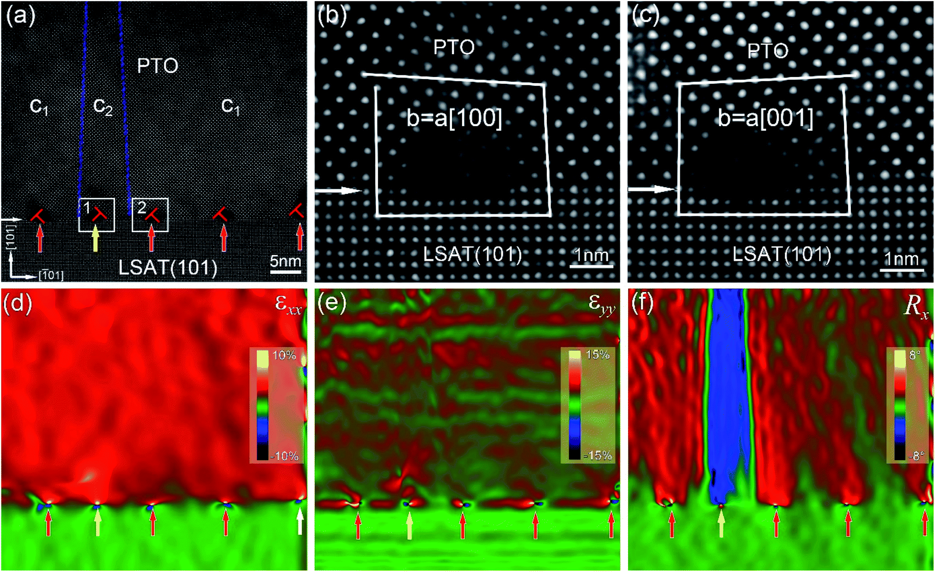 | ||
| Fig. 3 Atomic-scale dislocation cores and strain field analysis. (a) Low-magnification high-resolution HAADF-STEM image of a 50 nm PTO/LSAT(101) thin film. (b) and (c) Atomic-resolved HAADF-STEM images corresponding to two rectangle boxes labeled as “1” and “2” in (a), respectively. Note the two types of dislocation cores. (d)–(f) Strain distribution corresponding to the area of (a). (d) In-plane strain (εxx), (e) out-of-plane strain (εyy), and (f) lattice rotation (Rx). Note the same lattice rotation direction between the stripe 90° domains and misfit dislocations. | ||
For a more general view, a HAADF-STEM image including periodic stripe 90° c1/c2 domains in 50 nm PTO/LSAT(101) films was acquired and is shown in Fig. 4(a). Similarly, the blue dashed lines denote the 90° domain walls. The white arrow denotes the PTO/LSAT(101) interface. It can be seen that this area included four wide c1 domains and three narrow c2 domains. Fig. 4(b) and (c) show the in-plane strain (εxx) and lattice rotation (Rx) maps corresponding to the area in Fig. 4(a), respectively. In Fig. 4(b), many bright dots displaying strain fields of the interfacial misfit dislocations appear at the PTO/LSAT(101) interface. In Fig. 4(b), there is an obvious contrast difference between the wide c1 and narrow c2 domains, which is similar to the lattice rotation in Fig. 3(f). Besides, misfit dislocations existed at the bottom of each c domain, as shown in Fig. 4(c). With respect to the LSAT substrate, the wide c1 domains displayed a clockwise lattice rotation, while the narrow c2 domains featured an anticlockwise lattice rotation. The misfit dislocation cores (labeled as yellow arrows) exhibited a same clockwise lattice rotation with each wide c1 domain, while the misfit dislocation cores (labeled as red arrows) exhibited a same clockwise lattice rotation with each narrow c2 domain. It was surprising that the lattice rotation of the misfit dislocations behaved like it did in Fig. 3, which was consistent with the c domains above them, indicating that the phenomenon was ubiquitous. To further investigate the relationship between the polarization direction and Burgers vectors, an atomic-scale HAADF-STEM image of the area labeled as the white dashed rectangle box in Fig. 4(a) was recorded and is shown in Fig. 4(d). Two blue dashed lines denote the 90° domain walls. The yellow and red circles denote the Pb and Ti atom columns, respectively, based on the principle of HAADF-STEM imaging.36 The yellow arrows denote the reversed Ti-displacement (δTi). Fig. 4(e) gives the polarization map of PTO unit cells corresponding to the area of Fig. 4(d). The arrows denote reversed δTi, which was consistent with the polarization direction of PTO unit cells. It could be clearly seen that the polarization directions had an almost 90° rotation across the c1/c2 domain walls, forming a “head-to-tail” polarization configuration. Besides, the ferroelectric polarization in the narrow c2 domain exhibited a little rotation toward the in-plane direction, as shown in Fig. 4(e). Fig. 4(f) shows the polarization distribution of the stripe domains in Fig. 4(a). The polarization directions of the wide c1 domains were along the up left, while the polarization directions of the narrow c2 domains were along the down left. By drawing a Burgers circuit surrounding each dislocation core, the projected Burgers vectors on the (010) plane of the interfacial misfit dislocations were determined and are shown in Fig. 4(f). It was found that the Burgers vectors of all the misfit dislocations were parallel to the polarization directions of their above c domains.
 | ||
| Fig. 4 Periodic stripe 90° domains and interfacial misfit dislocation arrays. (a) Low-magnification high-resolution HAADF-STEM image of a 50 nm PTO/LSAT(101) thin film. (b) and (c) Strain distribution of the 50 nm PTO/LSAT(101) thin films corresponding to the area of (a). (b) In-plane strain (εxx), (c) lattice rotation (Rx). (d) Atomic-resolved HAADF-STEM images corresponding to the rectangle box in (a). Blue dashed lines denote the 90° domain walls. Yellow and red circles denote Pb and Ti atoms, respectively. Yellow arrows denote the reversed Ti-displacements (δTi), which were consistent with the polarization directions of PTO. (e) Polarization map of PTO unit cells corresponding to the area of (d). (f) Schematic diagram showing the relationship between the Burgers vectors of the misfit dislocations and the polarization directions of the 90° domains. | ||
Fig. 5(a) presents a low-magnification high-resolution HAADF-STEM image of the 70 nm PTO/LSAT(101) films. A white arrow denotes the PTO/LSAT(101) interface. The area labeled as a white rectangle box in Fig. 5(a) was selected and magnified, as shown in Fig. 5(b). The projected Burgers vectors of b = a[100] on the (010) plane were determined. Fig. 5(c) and (d) present the in-plane strain (εxx) and lattice rotation (Rx) maps corresponding to the area of Fig. 5(a), respectively. It can be seen that the domain walls were bent and ended at the inside of the PTO films when the PTO films were thicker, as shown in Fig. 5(d). Besides, at the bottom of the “V”-type c domain, a dislocation labeled as a yellow arrow was formed in the PTO films. Importantly, the upside of the dislocation displayed the same clockwise lattice rotation with the “V”-type c domain, indicating that the strain field coupling between the ferroelastic domains and dislocations in the PTO films remained.
 | ||
| Fig. 5 Dislocation core and strain field analysis in a 70 nm PTO/LSAT(101) film. (a) Low-magnification high-resolution HAADF-STEM image of the 70 nm PTO/LSAT(101) thin film. (b) Atomic-resolved HAADF-STEM images corresponding to the rectangle box in (a), showing the dislocation core inside the PTO films. (c) and (d) Strain distribution of the 70 nm PTO/LSAT(101) thin film, (c) in-plane strain (εxx), (d) lattice rotation (Rx). | ||
For exploring the effect of the misfit dislocations on the ferroelectric polarization, atomic-resolved HAADF-STEM images at dislocation cores corresponding to these areas labeled as rectangle boxes “1” and “2” in Fig. 4(a) were acquired and are displayed in Fig. 6(a) and (b), respectively. The two blue dashed lines in Fig. 6(a) denote the 90° domain walls. Fig. 6(c) shows the polarization configuration corresponding to the area above the misfit dislocation core marked by the red rectangle box in Fig. 6(a). The yellow arrows denote the polarization direction of the PTO unit cells. It could be seen that the polarizations of the PTO unit cells near the misfit dislocation (marked by red dashed ellipse) generated rotation toward the in-plane direction, while the polarizations of the above PTO unit cells marked by the blue dashed ellipse were still along the [00] direction, which revealed that the formation of this misfit dislocation influenced the ferroelectric polarization. Similarly, Fig. 6(d) shows the polarization configuration corresponding to the area above the misfit dislocation core marked by the red rectangle box in Fig. 6(b). The yellow arrows denote the polarization direction of the PTO unit cells. It could be noted that the polarizations of almost all the PTO unit cells in this area pointed to the [100] direction. Only a few PTO unit cells near the misfit dislocation exhibited a slight polarization deviation away from the [100] direction, as marked by the red dashed ellipse in Fig. 6(d).
 | ||
| Fig. 6 (a) and (b) Two atomic-resolved HAADF-STEM images corresponding to the white rectangular boxes labeled as “1” and “2” in Fig. 4(a), respectively. (c) and (d) Polarization maps corresponding to the red dashed rectangular boxes in (a) and (b), respectively. | ||
4. Discussion
For the [101]-oriented PTO/LSAT film system, the lattice mismatches along the in-plane two perpendicular directions of [01] and [010] were deduced to be −4.1% and −0.8%, respectively, which indicates the PTO films grown on the LSAT(101) substrates were constrained by asymmetric biaxial compressive strain.25 The inhomogeneous distribution of dislocation lines could be clearly seen in Fig. 2(e), which might be attributed to the inhomogeneous interface strain due to the asymmetric biaxial compressive strain imposed by the substrates.37 The formation of misfit dislocations plays an important role in the PTO/LSAT(101) film system. First, the in-plane strain field εxx of the PTO films (Fig. 3(d) and 4(b)) was up to about 4.0% compared with the LSAT(101) substrate, which indicates that the in-plane compressive strain of the PTO film was better relaxed by the formation of misfit dislocations. Second, the in-plane strain field εxx around the misfit dislocations exhibited a tensile and compressive state at the film and substrate side, respectively. At room temperature, the interplanar spacing d101 of PTO was larger than the d101 of the LSAT substrate. The in-plane strain field εxx of the misfit dislocations could be well matched with the lattice difference of the PTO films and LSAT(101) substrate. Last, the lattice rotation Rx of the misfit dislocations was consistent with their above c domains, as shown in Fig. 3(f) and 4(c). In general, lattice rotation is accompanied by shear strain in perovskite oxide thin films.15 Thus, it is evident that strain coupling between the ferroelastic 90° domains and misfit dislocations existed in the PTO/LSAT(101) thin film system.
As reported previously, the formation of misfit dislocations is a main approach for strain relaxation for [101]-/[111]-oriented ferroelectric films.28,29 In this work, we further reveal the strain coupling of ferroelastic domains and misfit dislocations, which may help to explore the nucleation and propagation mechanism of ferroelastic domains and further modify the high-quality growth of [101]-/[111]-oriented ferroelectric films. Besides, the thickness-dependent evolution of piezoelectric response with a critical size effect in the PTO/LSAT(101) thin film system was reported previously.25 Generally, the formation of misfit dislocations can induce polarization instability and degradation of the out-of-plane piezoelectric responses.7,38 On the one hand, the strain field around the dislocation cores generates a largely localized polarization gradient and leads to a strong depolarizing field to suppress the ferroelectric polarization near dislocation cores.38 On the other hand, the strain coupling of ferroelastic domains and misfit dislocations could lead to the pinning of the ferroelastic domain walls, which can restrict the ferroelastic domain walls motion under an applied electric field and hence reduce the extrinsic contribution to piezoelectric responses.38 Importantly, the strain coupling of ferroelastic domains and misfit dislocations could be used to modify the physical properties of perovskite oxide thin films in the future. For instance, the introduction of dislocation networks with alternate arrangements of these two types of dislocations may trigger ferroelectric polarization in [110]-oriented paraelectric STO films.
In addition, the polarization rotation of the PTO unit cells in the narrow near c2 domain in Fig. 4(e) may be attributed to a flexoelectric effect. The flexoelectric effect involves a coupling between the polarization and strain gradient.39 Fig. 7(a) shows a high-resolution HAADF-STEM image of the typical area including wide c1 and narrow c2 domains. The left red line denotes the (101) plane near the substrate. The left orange and yellow lines denote the (101) plane in the middle and near surface of the PTO films, respectively. It was found that the (101) planes in the wide c1 domain have a clockwise rotation from the substrate to surface side. Similarly, the (101) planes in the narrow c2 domain have an anticlockwise rotation from the substrate to surface side. The difference is that the rotation angle in the narrow c2 domain was larger than in the wide c1 domain. The different rotation angle of the (101) plane from the substrate to surface side may result from the constraints imposed by the LSAT substrates.40 Fig. 7(b) is a schematic of the stripe 90° c1/c2 domains with a wide c1 domain and a narrow c2 domain. The lattice rotation could generate a strain gradient along the in-plane direction of the out-of-plane strain εyy, which is denoted as  , as schematized in Fig. 7(b). The c1 domain was wider and the rotation angle smaller, which made that the strain gradient
  for the c1 domain be very small. On the contrary, the c2 domain was narrower and the rotation angle was larger, indicating that the strain gradient
  for the c2 domain was large. The flexoelectric polarization along the in-plane direction (Px(flexo)) was calculated by the following formula:41
 | (1) |
 | ||
| Fig. 7 (a) HAADF-STEM image including the wide c1 and narrow c2 domains of a 50 nm PTO/LSAT(101) film. (b) Schematic of the stripe 90° c1/c2 domains with a wide c1 domain and a narrow c2 domain. Yellow and red arrows denote the ferroelectric polarization and flexoelectric polarization, respectively. | ||
Importantly, the formation of misfit dislocation can generate a larger strain gradient (∼106/m) around a dislocation core, which triggers a larger flexoelectric polarization. Thus, the polarization of PTO unit cells in the narrow c2 domain was almost rotated to the in-plane directions around the misfit dislocation core (Fig. 6(c)). Besides, the flexoelectric polarization also induced a slight polarization rotation in the wide c1 domain around the misfit dislocation core (Fig. 6(d)). A similar phenomenon has been reported in multiferroic BiFeO3 films.30
5. Conclusions
In summary, [101]-oriented PTO films were deposited on LSAT(101) substrates by pulsed laser deposition (PLD). The strain fields and polarization configurations in the stripe 90° domains and nearby misfit dislocations were investigated using (scanning) transmission electron microscopy (TEM) and geometry phase analysis (GPA). Two types of mixed dislocations with the opposite lattice rotation were found to exist at the PTO/LSAT(101) interfaces, which generated different strain fields around dislocation cores. It was clarified that the strain fields of the two types of misfit dislocations coupled with the c domains above them. The flexoelectric-induced polarization rotation was revealed in the narrow c domains and nearby interfacial dislocation cores. These results may provide useful information for understanding the formation of ferroelastic domains and for the further high-quality growth of high-index ferroelectric thin films.Author contributions
Y. L. Z. and X. L. M. conceived the project of interfacial characterization in oxides by using aberration-corrected STEM. Y. P. F., Y. L. Z., and X. L. M. designed the experiments. Y. P. F. performed the thin-film growth and STEM observations. R. J. J. performed the XRD test of thin films. Y. L. T., M. J. Z. and W. R. G. participated in the thin-film growth and STEM imaging. Y. J. W. participated in data analysis. All authors contributed to the discussions and manuscript preparation.Conflicts of interest
There are no conflicts to declare.Acknowledgements
This work is supported by the National Natural Science Foundation of China (No. 51971223, 51922100 and 52122101), the Guangdong Basic and Applied Basic Research Foundation (No. 2021A1515110064), the Key Research Program of Frontier Sciences CAS (QYZDJ-SSW-JSC010) and Shenyang National Laboratory for Materials Science (L2019R06, L2019R08, L2019F01, L2019F13). Y. P. F. acknowledges the China National Postdoctoral Program for Innovative Talents (No. BX2021348) and the project funded by China Postdoctoral Science Foundation (No. 2021M703455). Y. L. T. acknowledges the Scientific Instrument Developing Project of CAS (YJKYYQ20200066). Y. J. W., Y. L. T. acknowledge the Youth Innovation Promotion Association CAS (No. 2021187, Y202048).References
- J. F. Scott, Science, 2007, 315, 954–959 CrossRef CAS PubMed
.
- N. Setter, D. Damjanovic, L. Eng, G. Fox, S. Gevorgian, S. Hong, A. Kingon, H. Kohlstedt, N. Y. Park, G. B. Stephenson, I. Stolitchnov, A. K. Taganstev, D. V. Taylor, T. Yamada and S. Streiffer, J. Appl. Phys., 2006, 100, 051606 CrossRef
- L. W. Martin and A. M. Rappe, Nat. Rev. Mater., 2016, 2, 16087 CrossRef
- D. G. Schlom, L.-Q. Chen, C.-B. Eom, K. M. Rabe, S. K. Streiffer and J.-M. Triscone, Annu. Rev. Mater. Res., 2007, 37, 589–626 CrossRef CAS
- D. G. Schlom, L.-Q. Chen, C. J. Fennie, V. Gopalan, D. A. Muller, X. Pan, R. Ramesh and R. Uecker, MRS Bull., 2014, 39, 118–130 CrossRef CAS
- S. C. Jain, A. H. Harker and R. A. Cowley, Philos. Mag. A, 1997, 75, 1461–1515 CAS
- M. W. Chu, I. Szafraniak, R. Scholz, C. Harnagea, D. Hesse, M. Alexe and U. Gosele, Nat. Mater., 2004, 3, 87–90 CrossRef CAS PubMed
- S. P. Alpay, I. B. Misirlioglu, V. Nagarajan and R. Ramesh, Appl. Phys. Lett., 2004, 85, 2044–2046 CrossRef CAS
- C. L. Jia, S. B. Mi, K. Urban, I. Vrejoiu, M. Alexe and D. Hesse, Phys. Rev. Lett., 2009, 102, 117601 CrossRef CAS PubMed
- H. H. Wu, J. Wang, S. G. Cao and T. Y. Zhang, Appl. Phys. Lett., 2013, 102, 232904 CrossRef
- Y. L. Tang, Y. L. Zhu, Y. Liu, Y. J. Wang and X. L. Ma, Nat. Commun., 2017, 8, 15994 CrossRef CAS PubMed
- M. Hofling, X. Zhou, L. M. Riemer, E. Bruder, B. Liu, L. Zhou, P. B. Groszewicz, F. Zhuo, B. X. Xu, K. Durst, X. Tan, D. Damjanovic, J. Koruza and J. Rodel, Science, 2021, 372, 961–964 CrossRef PubMed
- S. Hameed, D. Pelc, Z. W. Anderson, A. Klein, R. J. Spieker, L. Yue, B. Das, J. Ramberger, M. Lukas, Y. Liu, M. J. Krogstad, R. Osborn, Y. Li, C. Leighton, R. M. Fernandes and M. Greven, Nat. Mater., 2022, 21, 54–61 CrossRef CAS PubMed
- Y. L. Li, S. Y. Hu, Z. K. Liu and L. Q. Chen, Acta Mater., 2002, 50, 395–411 CrossRef CAS
- Y. L. Tang, Y. L. Zhu and X. L. Ma, Ultramicroscopy, 2016, 160, 57–63 CrossRef CAS PubMed
- J. Ma, Y. Zhu, Y. Tang, M. Han, Y. Wang, N. Zhang, M. Zou, Y. Feng, W. Geng and X. Ma, RSC Adv., 2019, 9, 13981–13990 RSC
- G. Catalan, A. Lubk, A. H. Vlooswijk, E. Snoeck, C. Magen, A. Janssens, G. Rispens, G. Rijnders, D. H. Blank and B. Noheda, Nat. Mater., 2011, 10, 963–967 CrossRef CAS PubMed
- D. Su, Q. Meng, C. A. F. Vaz, M.-G. Han, Y. Segal, F. J. Walker, M. Sawicki, C. Broadbridge and C. H. Ahn, Appl. Phys. Lett., 2011, 99, 102902 CrossRef
- P. Gao, C. T. Nelson, J. R. Jokisaari, S. H. Baek, C. W. Bark, Y. Zhang, E. Wang, D. G. Schlom, C. B. Eom and X. Pan, Nat. Commun., 2011, 2, 591 CrossRef PubMed
- M.-W. Chu, I. Szafraniak, D. Hesse, M. Alexe and U. Gösele, Phys. Rev. B: Condens. Matter Mater. Phys., 2005, 72, 174112 CrossRef
- T. Kiguchi, K. Aoyagi, Y. Ehara, H. Funakubo, T. Yamada, N. Usami and T. J. Konno, Sci. Technol. Adv. Mater., 2011, 12, 034413 CrossRef PubMed
- J. Ouyang, J. Slusker, I. Levin, D. M. Kim, C. B. Eom, R. Ramesh and A. L. Roytburd, Adv. Funct. Mater., 2007, 17, 2094–2100 CrossRef CAS
- R. J. Xu, J. Karthik, A. R. Damodaran and L. W. Martin, Nat. Commun., 2014, 5, 3120 CrossRef PubMed
- R. J. Xu, S. Liu, I. Grinberg, J. Karthik, A. R. Damodaran, A. M. Rappe and L. W. Martin, Nat. Mater., 2015, 14, 79–86 CrossRef CAS PubMed
- Y. P. Feng, Y. L. Tang, D. S. Ma, Y. L. Zhu, M. J. Zou, M. J. Han, J. Y. Ma and X. L. Ma, ACS Appl. Mater. Interfaces, 2018, 10, 24627–24637 CrossRef CAS PubMed
- M. J. Zou, Y. L. Tang, Y. L. Zhu, Y. P. Feng, Y. J. Wang, M. J. Han, N. B. Zhang, J. Y. Ma, B. Wu and X. L. Ma, Acta Mater., 2019, 166, 503–511 CrossRef CAS
- W. R. Geng, X. W. Guo, Y. L. Zhu, Y. L. Tang, Y. P. Feng, M. J. Zou, Y. J. Wang, M. J. Han, J. Y. Ma, B. Wu, W. T. Hu and X. L. Ma, ACS Nano, 2018, 12, 11098–11105 CrossRef CAS PubMed
- Y. Feng, Y. Tang, Y. Zhu, M. Zou and X. Ma, J. Mater. Res., 2018, 33, 4156–4164 CrossRef CAS
- Y. B. Xu, Y. L. Tang, Y. L. Zhu, Y. Liu, S. Li, S. R. Zhang and X. L. Ma, Sci. Rep., 2016, 6, 35172 CrossRef CAS PubMed
- W. R. Geng, Y. J. Wang, Y. L. Tang, Y. L. Zhu, B. Wu, L. X. Yang, Y. P. Feng, M. J. Zou and X. L. Ma, Nano Lett., 2021, 21, 9601–9608 CrossRef CAS PubMed
- S. M. Anthony and S. Granick, Langmuir, 2009, 25, 8152–8160 CrossRef CAS PubMed
- Y. L. Tang, Y. L. Zhu, X. L. Ma, A. Y. Borisevich, A. N. Morozovska, E. A. Eliseev, W. Y. Wang, Y. J. Wang, Y. B. Xu, Z. D. Zhang and S. J. Pennycook, Science, 2015, 348, 547–551 CrossRef CAS PubMed
- Y. J. Wang, Y. P. Feng, Y. L. Zhu, Y. L. Tang, L. X. Yang, M. J. Zou, W. R. Geng, M. J. Han, X. W. Guo, B. Wu and X. L. Ma, Nat. Mater., 2020, 19, 881–886 CrossRef PubMed
- A. M. Glazer and S. A. Mabud, Acta Crystallogr., Sect. B: Struct. Crystallogr. Cryst. Chem., 1978, 34, 1065–1070 CrossRef
- D. Mateika, H. Kohler, H. Laudan and E. Volkel, J. Cryst. Growth, 1991, 109, 447–456 CrossRef CAS
- S. J. Pennycook and D. E. Jesson, Ultramicroscopy, 1991, 37, 14–38 CrossRef
- Y. L. Tang, Y. L. Zhu, H. Meng, Y. Q. Zhang and X. L. Ma, Acta Mater., 2012, 60, 5975–5983 CrossRef CAS
- V. Nagarajan, C. L. Jia, H. Kohlstedt, R. Waser, I. B. Misirlioglu, S. P. Alpay and R. Ramesh, Appl. Phys. Lett., 2005, 86, 192910 CrossRef
- P. Zubko, G. Catalan and A. K. Tagantsev, Annu. Rev. Mater. Res., 2013, 43, 387–421 CrossRef CAS
- Y. Feng, H. Zhang, Y. Zhu, Y. Wang, Y. Tang, M. Zou, M. Han, W. Geng, J. Ma and X. Ma, J. Phys. Chem. C, 2019, 123, 19602–19609 CrossRef CAS
- Y.-J. Wang, J. Li, Y.-L. Zhu and X.-L. Ma, J. Appl. Phys., 2017, 122, 224101 CrossRef
| This journal is © The Royal Society of Chemistry 2022 |