DOI:
10.1039/D2RA03411E
(Paper)
RSC Adv., 2022,
12, 22984-22995
Efficient and stable perovskite solar cells using manganese-doped nickel oxide as the hole transport layer†
Received
1st June 2022
, Accepted 9th August 2022
First published on
16th August 2022
Abstract
Organic/inorganic hybrid perovskite solar cells (PSCs) have represented a promising field of renewable energy in recent years due to the compelling advantages of high efficiency, facile fabrication process and low cost. The development of inorganic p-type metal oxide materials plays an important role in the performance and stability of PSCs for commercial purposes. Herein a facile and effective way to improve hole extraction and conductivity of NiOx films by manganese (Mn) doping is demonstrated in this study. A Mn-doped NiOx layer was prepared by the sol–gel process and served as the hole transport layer (HTL) in inverted PSCs. The results suggest that Mn-doped NiOx is helpful for the growth of perovskite layers with larger grains and higher crystallinity compared with the pristine NiOx. Furthermore, the perovskite films deposited on Mn-doped NiOx exhibit lower recombination and shorter carrier lifetime. The device based on 0.5 mol% Mn-doped NiOx as the HTL displayed the best power conversion efficiency (PCE) of 17.35% and a high fill factor (FF) of 81%, which were significantly higher than those of the one using the pristine NiOx HTL (PCE = 14.71%, FF = 73%). Moreover, the device retained 70% of its initial efficiency after 35 days' storage under a continuous halogen lamp matrix exposure with an illumination intensity of 1000 W m−2. Our results widen the development of PSCs for future production.
1. Introduction
Photovoltaic cells based on perovskite materials have attracted a great deal of attention from academic and industrial researchers owing to their advantageous features of high absorption behavior in the visible spectrum, long carrier diffusion length, high carrier mobility, low exciton binding energy, tunable bandgaps by exchanging materials composition, and low fabrication cost.1–5 The power conversion efficiency (PCE) of perovskite solar cells (PSCs) has been remarkably developed from 3.8% to 25.5% within a decade.6,7 The PCE of PSCs has exceeded that of inorganic thin-film photovoltaics on a laboratory scale and is comparable to that of commercialized silicon solar cells by miscellaneous techniques, including optimization of device structure, interface engineering, and passivation of materials.8–10
The chemical formula of perovskite absorbing materials is ABX3, where A stands for an organic–inorganic monovalent cation, B symbolizes a divalent metal cation, and X represents a monovalent anion.11 Single cationic perovskite materials like methylammonium lead iodide (MAPbI3) and formamidinium lead iodide (FAPbI3) have been utilized as the active layer in PSCs with PCE values up to 18.7% and 17.11%, respectively.12,13 However, the PSCs based on single cationic perovskite materials usually encounter unavoidable drawback of poor thermal and humidity stability that limits their further development in photovoltaic application.14 In order to solve these problems and achieve high device performance, Yi et al. proposed a mixed cation perovskite CsxFA1−xPbX3 as the light absorber in PSCs.15 The material possesses good thermal stability over the investigated temperature range of 20 to 250 °C and the optimized device exhibited a high PCE of 17.35% as well as long-term stability of 1000 hours in the dark under ambient environment without encapsulation. Saliba et al. incorporated a mixture of a triple Cs/MA/FA cation into perovskite absorbing layer, confirming an initial PCE of 21.1% and a stabilized PCE of 18% after 250 hours of aging under full illumination in a nitrogen atmosphere at room temperature.16 Obviously, the adoption of multiple cation perovskite materials is essential for PSCs to enter global photovoltaic market in the future.
The inverted PSC with p–i–n structure of anode/hole transport layer (HTL)/perovskite/electron transport layer (ETL)/cathode has been extensively developed within a decade because of its simple device structure, little hysteresis effect and free of high-temperature processing.17 Besides, PSCs can be combined with silicon-based, copper indium gallium selenide, or other kinds of solar cells to construct high-efficiency solar cells with tandem structures.18–20 Poly(3,4-ethylenedioxythiophene):poly(styrene sulfonate) (PEDOT:PSS) has been widely used as the HTL in inverted PSCs owing to the advantages of easy processing and matched energy level with the perovskite.21,22 However, it is also reported that the hygroscopic and acidic nature of PEDOT:PSS may deteriorate the transparent conducting oxide electrode, such as fluorine-doped tin oxide (FTO) and indium tin oxide (ITO), leading to degradation of device performance.23,24 In contrast to organic PEDOT:PSS, inorganic p-type nickel oxide (NiOx) has been extensively employed as the HTL because of its superior hole extraction ability, high transmittance in the visible range, and environmental stability.25,26 Until now, there have been several methods to prepare NiOx HTL for inverted PSCs, such as sol–gel deposition, atomic layer deposition, spray pyrolysis, and nanoparticle dispersion.27–30 The intrinsic hole mobility of solution-processed NiOx is reported to be 10−5 to 10−3 cm2 V−1 s−1,31 and therefore doping process is usually adopted to increase holes mobility and hole extraction ability associated with reduced carrier recombination to achieve higher device performance of PSCs.32 Teo et al. reported inverted PSCs using La-doped NiOx as the HTL and the reduction in internal resistance resulted in enhanced conductivity of the HTL after La doping.33 The PSC based on 3 mol% La-doped NiOx displayed a promising PCE of 15.46% and retained 95% of its initial PCE after 50 days storage in a moisture-free desiccator. Park et al. demonstrated solution-processed Li-doped NiOx as the HTL in PSCs.34 The improved electrical conductivity of NiOx was confirmed by conductive atomic force microscope, and the device based on 5% Li-doped NiOx exhibited an average PCE of 14.66%, which was improved by 21% compared to the pristine NiOx. Thiruchelvan et al. utilized the solution-processed Zn-doped NiOx as the HTL for fabricating inverted PSCs with an average PCE of 14.67%.35 They found that Zn doping is able to improve carrier extraction and conductivity without any negative effect on the optical properties of NiOx. Apart from single doping, some researchers select co-doping to further improve conductivity of NiOx layers. For example, Zn–Ce, Li–Co or Li–Co–Mg dopants have been incorporated into NiOx as the HTL and the corresponding PSCs showed enhanced PCE values from 7.47–17.4% to 13.22–20.1%.36–38 The introducing amounts of different dopants should be carefully controlled to prevent overdosed doping that usually reduces device performance.
In this study, manganese(II) acetate tetrahydrate was firstly chosen as an additive to form Mn-doped NiOx film as the HTL in PSCs. Different molar ratio of the Mn dopant from 0.5 to 2 mol% was incorporated to investigate the effect of Mn doping on the morphological, optical and electrical properties of the NiOx HTL. As mentioned in the previous part, ion doping can enhance carrier extraction ability and conductivity of metal oxide semiconductors. Besides, Mn-containing perovskite materials have been reported to serve as the light absorbing layer for the fabrication of PSCs,39 implying that Mn ions would not damage the perovskite layer even if Mn ions are released from NiOx lattice. To fabricate highly efficient inverted PSCs, 6,6-phenyl-C61-butyric acid methyl ester (PC61BM) was chosen as the ETL and tetrabutylammonium tetrafluoroborate (TBABF4) was doped to improve electron extraction of PC61BM. Furthermore, polyethylenimine (PEI) was incorporated as the interfacial layer between PC61BM and Ag electrode. The inverted devices with the architecture of FTO/un-doped or Mn-doped NiOx/perovskite/PC61BM + TBABF4/PEI/Ag were fabricated and evaluated. The best PCE value of 17.35% was obtained using 0.5 mol% Mn-doped NiOx as the HTL. Moreover, the device under the halogen lamps matrix irradiation with an illumination intensity of 1000 W m−2 sustained 70% of its initial efficiency after 35 days storage, which reveals better stability than the control device using pristine NiOx HTL.
2. Experimental section
2.1. Materials
FTO-coated glass substrates were bought from Ruilong Optoelectronics Technology Co., Ltd. Nickel acetate tetrahydrate (purity 98+%) and manganese(II) acetate tetrahydrate (purity 99%) were purchased from Alfa Aesar and Showa, respectively. Ethanolamine (purity 99%) and TBABF4 (purity 98%) were purchased from Acros. High-purity perovskite precursors including lead bromide (PbBr2, purity 99.99%), lead iodide (PbI2, purity 99.9985%) and cesium iodide (CsI, purity 99.9%) were bought from Alfa Aesar. Formamidinium iodide (FAI, purity 98%) was purchased from STAREK Scientific Co. Ltd. from Taiwan. Methylammonium bromide (MABr, purity 98%) was bought from TCI. PC61BM (purity 99%) was purchased from Solenne B. V., Netherlands. PEI (molecular weight 25![[thin space (1/6-em)]](https://www.rsc.org/images/entities/char_2009.gif) 000) was bought from Sigma-Aldrich. Other solvents were purchased from Alfa Aesar or Acros and used without further purification.
000) was bought from Sigma-Aldrich. Other solvents were purchased from Alfa Aesar or Acros and used without further purification.
2.2. Preparation of the un-doped and Mn-doped NiOx layers
The NiOx precursor solution was prepared according to previous literature with some modified parameters.27 A mixture of 0.124 g of nickel acetate tetrahydrate, 30 µL of ethanolamine, and 5 mL of ethanol was heated at 70 °C with stirring in a sealed glass vial overnight. The color of the precursor solution became semitransparent green after dissolution. For Mn doping, 0.5 to 2 mol% of manganese(II) acetate tetrahydrate relative to nickel acetate tetrahydrate were added. The un-doped or Mn-doped NiOx layers were deposited on the FTO substrates from their precursor solutions by spin coating at 3000 rpm for 30 s, followed by drying at 80 °C for 10 min. Afterward, the samples were transferred to a high temperature oven and sintered at 450 °C for 1 hour to obtain the un-doped or Mn-doped NiOx layers.
2.3. Preparation of perovskite layers
The composition of the utilized perovskite in this research is Cs0.05FA0.81MA0.14Pb(Br0.15I0.85)3.40 To prepare its precursor solution, a mixture of MABr (21.8 mg), PbBr2 (77.1 mg), FAI (190.2 mg), PbI2 (548.6 mg), and CsI (17.5 mg) in 1 mL of a mixed solvent consisting of dimethyl sulfoxide (DMSO) and N,N-dimethylformamide (DMF) with 1:4 volume ratio was heated at 70 °C with stirring in a sealed glass vial for 1 hour, followed by filtration with 0.22 µm PTFE filters. The perovskite layer was deposited by spin coating in a nitrogen-filled glovebox in two steps: the first step was set at 1200 rpm for 10 s and the second step was set at 4500 rpm for 20 s. During the second step, 300 µL of ethyl acetate was dripped on the spinning substrate and the color of the perovskite layer became brown immediately. The deposited thin film was then annealed at 105 °C for 1 hour and dark brown perovskite layer was observed.
2.4. Device fabrication
The device structure of PSCs in this study is FTO/un-doped or Mn-doped MiOx/perovskite/PC61BM + TBABF4/PEI/Ag. FTO-coated glass substrates were cleaned in advance in detergent, deionized water, acetone, and isopropanol (IPA) for 10 min each under ultra-sonication, followed by UV-ozone exposure for 25 min. Next, un-doped or Mn-doped NiOx HTLs were deposited on the FTO substrates according to the procedure in the 2.2 section. Afterward, the deposition of the perovskite layer was referred to the procedure in the 2.3 section. The PC61BM solution (20 mg mL−1) containing 2 mol% of TBABF4 in chlorobenzene was spin-coated on the perovskite layer at 3000 rpm for 30 s, followed by heating at 100 °C for 10 min. 0.1 mol% of PEI in anhydrous IPA was then spin-coated on the PCBM layer at 5000 rpm for 30 s. Finally, 100 nm of Ag electrodes were deposited by thermal evaporation at a base pressure of 6 × 10⁻⁶ torr. The active area of each device was defined by a shadow mask with an open area of 4.5 mm2. Besides, hole- and electron-only devices with the configuration of FTO/un-doped or Mn-doped NiOx/Ag and FTO/PC61BM + TBABF4/PEI/Ag were fabricated, respectively, and their current–voltage (I–V) characteristics were measured for comparison.
2.5. Characterization
The I–V characteristics of hole- and electron-only devices were measured using a Keithley 2400 sourcemeter. The transmission spectra of samples were recorded by a Princeton Instruments Acton 2150 spectrophotometer, using a xenon lamp (ABET Technologies LS 150) as the light source. X-ray photoelectron spectroscopy (XPS) measurements were conducted by a Thermo Scientific K-Alpha X-ray photoelectron spectrometer for elemental composition analysis of NiOx with or without Mn doping. Kelvin probe force microscopy (KPFM) was performed using a Bruker Dimension ICON instrument. Ultraviolet photoelectron spectroscopy (UPS) measurements for the un-doped and Mn-doped NiOx films were performed on a Thermo VG-Scientific/Sigma Probe spectrometer. He I (hν = 21.22 eV) discharge lamp was used as the excitation source. The cross-sectional and top-view morphologies of samples were investigated with an ultrahigh resolution ZEISS Crossbeam scanning election microscope (SEM). X-ray diffraction (XRD) patterns and crystallinity of samples were measured by a Rigaku D/MAX2500 X-ray diffractometer. The steady-state photoluminescence (PL) were measured using an Oxford Instruments ANDOR Kymera 193i-B1 spectrograph. An Omicron QuixX 473-100 PS laser with an excitation wavelength at 473 nm was utilized as the light source. To perform time-resolved PL (TR-PL) measurements, a 473 nm pulsed laser (Omicron) was utilized as an excitation light source. The TR-PL signals were recorded by a time-correlated single-photon counting module (PicoQuant MultiHarp 150 4N) combined with a photomultiplier tube through an Andor Kymera 328i spectrometer. The apparatus was assembled by LiveStrong Optoelectronics Co., Ltd. from Taiwan. The current density–voltage (J–V) characteristics of PSCs were measured using a Keithley 2400 sourcemeter under AM 1.5G simulated sunlight exposure (Yamashita Denso YSS-100A equipped with a Xenon Short Arc lamp 1000 W) at 100 mW cm−2 under ambient environment. The external quantum efficiency (EQE) measurements were performed on a PV Measurement QE-R instrument which was assembled by Enli Technology Co., Ltd. from Taiwan. To investigate the stability of devices, encapsulated PSCs were constantly exposed to a halogen lamps matrix with an illumination intensity of 1000 W m−2 at room temperature with 40–70% relative humidity and their J–V characteristics were measured in each 24-h period.
3. Results and discussion
3.1. Characterization of the un-doped and Mn-doped NiOx
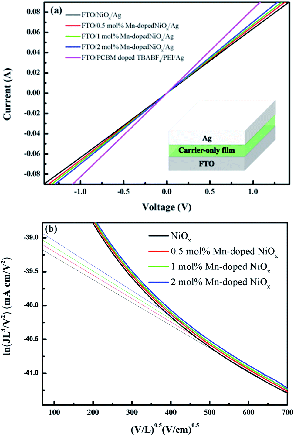
The effect of Mn doping on the single-charge mobility and conductivity of NiOx was studied from the I–V measurements of the carrier-only devices. Fig. 1(a) depicts the I–V characteristics of the hole-only FTO/un-doped or Mn-doped NiOx/Ag and electron-only FTO/PC61BM + TBABF4/PEI/Ag devices, while the inset shows the corresponding device structure. It is clearly seen that Mn-doped NiOx device possesses higher slope than the un-doped one, meaning that Mn doping can enhance conductivity and charge transport ability of NiOx. The conductivity of the hole-only device increased with increasing the concentration of Mn dopant. Besides, we notice that the hole-only devices based on Mn-doped NiOx showed closer conductivity to the electron-only device FTO/PC61BM + TBABF4/PEI/Ag, implying that equivalent carriers transport capabilities were achieved, and therefore the hysteresis effect in our final p-i-n device of FTO/Mn-doped NiOx/perovskite/PC61BM + TBABF4/PEI/Ag could be reduced. The hole mobility (µh) of NiOx films was approximated from the space charge limited current (SCLC) model defined as follows,41where J is the current density; V is the bias voltage; ε0 and ε are the vacuum dielectric constant and the relative dielectric constant of NiOx, respectively; L is the thickness of the NiOx film (∼30 nm). The curves of ln(JL3/V2) versus electric field (V/L)0.5 were derived by the SCLC model and displayed in Fig. 1(b).42 The µh of 0.5, 1 and 2 mol% Mn-doped NiOx was estimated to be 8.77 × 10⁻³, 9.45 × 10⁻³, and 1.07 × 10⁻² cm2 V−1 s−1, respectively, which was higher than the un-doped NiOx (8.22 × 10⁻³ cm2 V−1 s−1). The augmented µh value of Mn-doped NiOx is expected to bring on Jsc enhancement which is beneficial to device performance of PSCs.
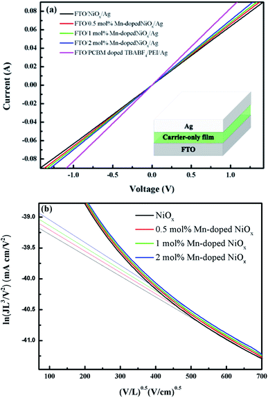 |
| | Fig. 1 (a) Linear sweep voltammetry curves of devices based on TBABF4-doped PCBM/PEI, un-doped and 0.5–2 mol% Mn-doped NiOx; (b) hole mobility of the un-doped and 0.5–2 mol% Mn-doped NiOx versus electric field (V/L)0.5. | |
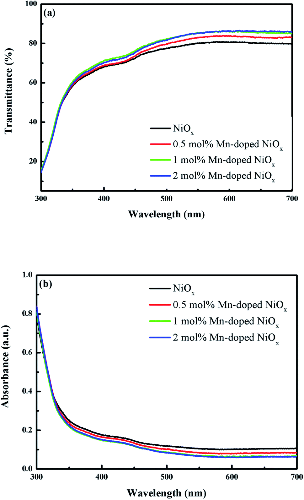
The transmission and absorption experiments were carried out to realize the optical spectra of the un-doped and Mn-doped NiOx on the FTO substrate, as depicted in Fig. 2. The transmittance of the un-doped NiOx in Fig. 2(a) was observed to be 68% at 400 nm and 80% at 600 nm. It can be seen that the transmittance of NiOx increases as the concentration of Mn dopant increases. The Mn-doped NiOx films have higher transmittance of 69–71% at 400 nm and even higher transmittance of 84–86% at 600 nm, indicative of anti-reflection phenomenon through Mn doping. Furthermore, higher transmittance of the Mn-doped NiOx HTL in the visible range facilitates incident photons to pass through and to be absorbed by the perovskite layer. Fig. 2(b) displays the absorption spectra of the un-doped and Mn-doped NiOx films. The optical bandgaps (Eg) of NiOx films can be derived from their absorption edge around 350 nm to be ca. 3.54 eV that is consistent with previous reports.25,43 It is clearly seen that the Eg of NiOx was not significantly affected by Mn doping. Besides, a slight absorption band was observed at 420 nm, indicative of Ni3+ species.44,45
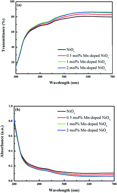 |
| | Fig. 2 (a) Transmission and (b) absorption spectra of the un-doped and 0.5–2 mol% Mn-doped NiOx films deposited on the FTO substrates. | |
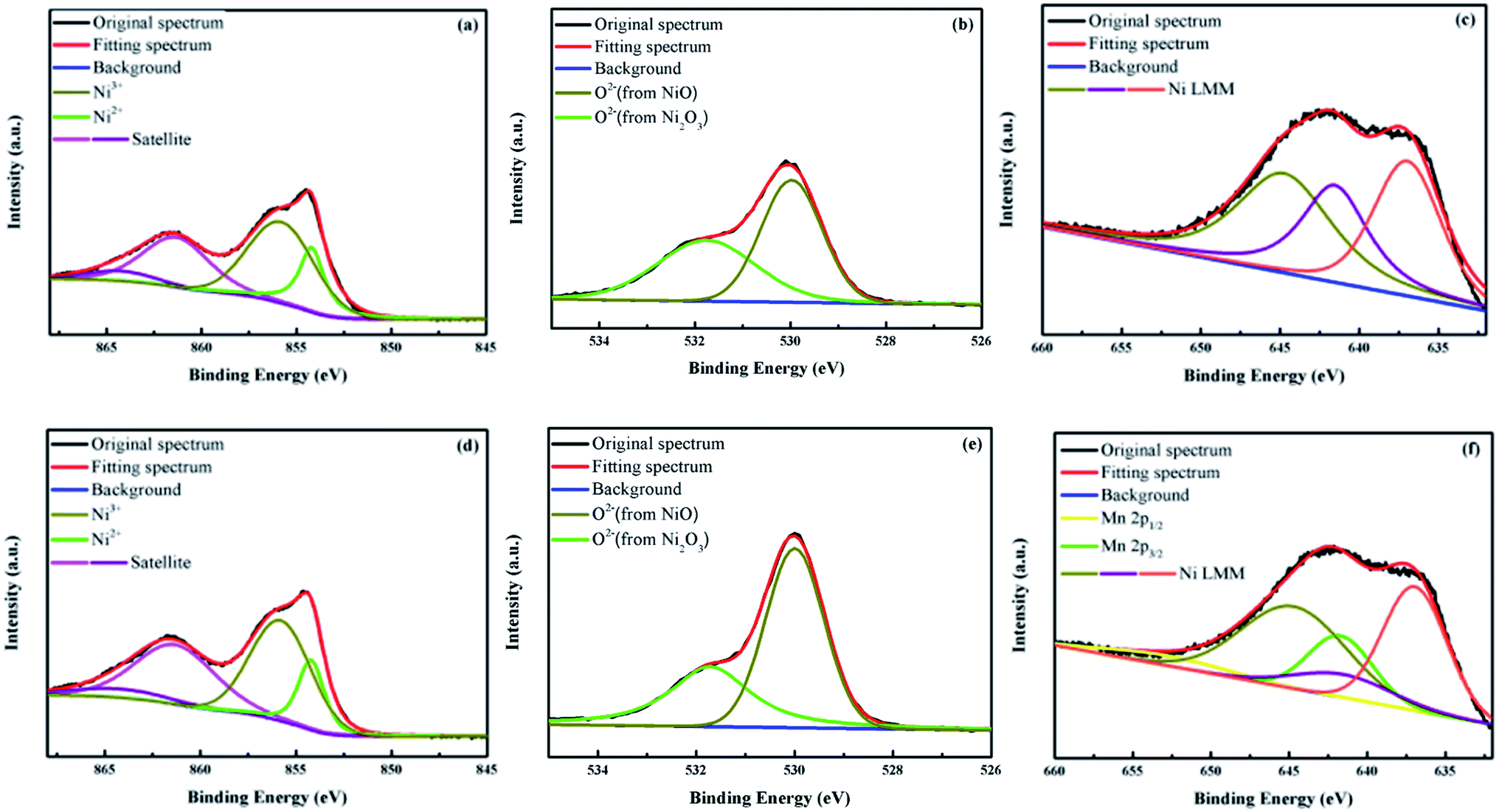
The XPS measurements were employed to investigate the elemental properties of Ni, O, and Mn atoms in the un-doped and 0.5% Mn-doped NiOx films. It is well known that hole transport ability of nonstoichiometric NiOx comes from the existence of Ni3+ (Ni2O3 species) in the crystalline structure.46 The high-resolution Ni 2p3/2 spectra for the un-doped and Mn-doped NiOx are displayed in Fig. 3(a) and (d), respectively, and the multicomponent band was deconvoluted into four different states at 854.2 (Ni2+), 855.8 (Ni3+), 861.34 (Ni2+ satellite), and 864.25 eV (Ni3+ satellite), which are in agreement with previous literature.47–49 The Ni3+/Ni2+ ratios for the un-doped and Mn-doped NiOx films were calculated to be 2.21 and 2.26, respectively. The slightly increased Ni3+ concentration in the Mn-doped NiOx indicates that the incorporated Mn2+ ions occupied the original Ni2+ sites, inducing Ni2+ to convert into Ni3+ to keep electroneutrality of NiOx. Similar phenomenon has been reported by Wang, Sun and their co-workers who utilized Mg-doped NiOx as the HTL for perovskite photodetectors.26 In this work, the increased Ni3+/Ni2+ ratio means that Mn doping promotes hole transport ability of NiOx.50 The high-resolution O 1s spectra of the un-doped and Mn-doped NiOx are presented in Fig. 3(b) and (e), respectively. By deconvoluting the O 1s signal, two prominent peaks at 530 and 531.7 eV are observed that are attributed to the NiO and Ni2O3 species, respectively.49 Fig. 3(c) and (f) demonstrate the Mn 2p spectra of the un-doped and Mn-doped NiOx, respectively. The above Mn 2p3/2 signal is embedded within the Ni LMM signal in the range of 640 and 644.7 eV and it is necessary to deconvolute the whole spectrum to find out its real location.51 No Mn 2p signal was found in Fig. 3(c), while Mn 2p3/2 and Mn 2p1/2 signals are located at 641.7 and 652.8 eV, as shown in Fig. 3(f).52 The observation of the two Mn 2p signals proves that Mn atoms were successfully integrated into the NiOx lattice.
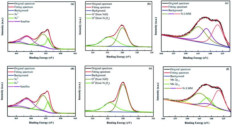 |
| | Fig. 3 XPS spectra of (a) (d) Ni 2p3/2, (b) (e) O 1s, and (c) (f) Mn 2p elements in the un-doped (upper row) and 0.5 mol% Mn-doped NiOx (lower row). | |
To realize the effect of Mn doping on the work function (φw) of NiOx films, KPFM technique was performed and the contact potential difference (CPD) distribution images of the un-doped and 0.5 mol% Mn-doped NiOx films are presented in Fig. 4(a) and (b), respectively.53 The CPD is determined by the interaction force between sample surface and a Pt-coated conductive cantilever probe, which is defined as CPD = (φtip − φsample)/−e and e is the electronic charge.54 The CPD variation for the un-doped NiOx film was found to be unevenly distributed between 65.3 and 127.6 mV, whereas that for the 0.5 mol% Mn-doped NiOx film was homogeneously distributed between a smaller scale range of −24.4 and 15 mV. Moreover, the φw difference between the un-doped and 0.5 mol% Mn-doped NiOx is estimated by the CPD to be 0.094 eV from KPFM experiment. It is seen that Mn doping can bring a lower surface potential profile and an up-shifted φw of NiOx film. To further confirm the φw and energy levels of NiOx films, UPS experiments were conducted and the acquired spectra are shown in Fig. 4(c) and (d). The φw can be derived by subtracting the binding energy cutoff in the high binding energy region (around 17 eV) from the monochromatic He I photon energy (21.22 eV). It is known that the φw is defined as the energy difference between the Fermi level (EF) and the vacuum level (0 eV). Therefore, the EF of the un-doped NiOx is calculated to be −4.02 eV from Fig. 4(c). By adding 0.5, 1 and 2 mol% Mn dopants, the EF of the modified NiOx are estimated to be −3.87, −3.75, and −3.6 eV, respectively. The low binding energy cutoff (around 1 eV) is related to the energy difference between the EF and valence band (VB). As a result, the VB of the un-doped and 0.5–2 mol% Mn-doped NiOx are derived to be −4.89, −4.93, −5.01, and −5.01 eV from Fig. 4(d), respectively. A downward shift of VB by Mn doping is beneficial to charge extraction and photovoltaic performance due to better energy level alignment between NiOx HTL and perovskite layer (VB ∼ −5.4 eV).55
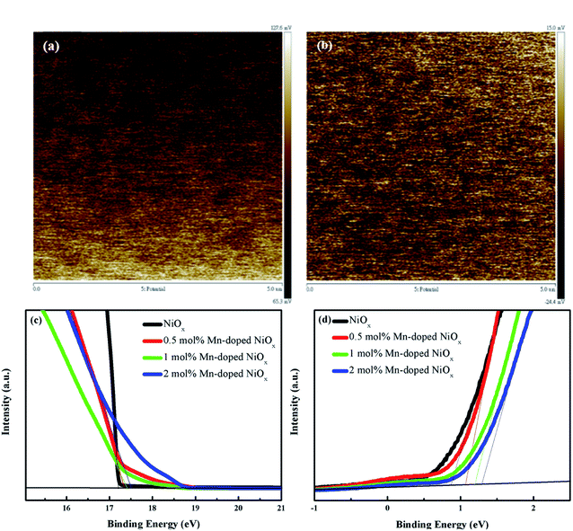 |
| | Fig. 4 KPFM images of the (a) un-doped and (b) 0.5 mol% Mn-doped NiOx on the FTO substrates; UPS spectra of the un-doped and 0.5–2 mol% Mn-doped NiOx at (c) high and (d) low binding energy region. | |
To discuss the effect of Mn doping on the surface morphology and crystallinity of NiOx, top-view SEM images as well as XRD patterns of the un-doped and Mn-doped NiOx were obtained as Fig. S1 and S2 in the ESI,† respectively. Very thin NiOx layers were deposited on the FTO substrates and the grains of low-lying FTO are clearly seen. It is difficult to verify whether Mn doping affects the morphology of NiOx. In Fig. S2,† all samples show three diffraction peaks at 2θ = 37.0, 43.3, and 62.9°, which corresponds to (111), (200), and (220) planes.50,56 Besides, no additional diffraction peak was formed upon Mn doping, indicating that the crystallinity of NiOx was not altered in the doping process.
3.2. Characterization of perovskite layers on NiOx
Fig. 5 reveals the top-view SEM images of the perovskite on the un-doped and Mn-doped NiOx layers. It is clearly seen that the perovskites on the Mn-doped NiOx have larger grains compared with that on the un-doped NiOx. The larger perovskite crystals are helpful for reducing charge recombination, which ensures effective carrier extraction and transport.57 In addition to SEM observation, XRD experiment was carried out to analyze the crystallinity of perovskites on different NiOx. Fig. 6 demonstrates the XRD patterns of perovskite layers on the un-doped and 0.5 mol% Mn-doped NiOx. Several intense diffraction peaks are observed at 2θ = 14.08, 19.94, 24.54, 28.4, 31.81, 34.91, 40.64, and 43.17°, corresponding to (001), (011), (111), (002), (012), (112), (022), and (003) planes of the perovskite Cs0.05FA0.81MA0.14Pb(Br0.15I0.85)3. The diffraction peaks of the prepared perovskites in this study are consistent with previous reports.49,58 Furthermore, the perovskite on the 0.5 mol% Mn-doped NiOx shows stronger diffraction signals than that on the pristine NiOx, implying that Mn-doped NiOx is profitable for the growth of perovskite layers with higher crystallinity.
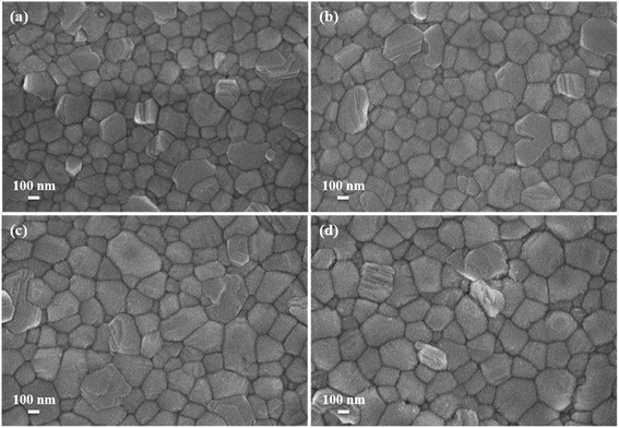 |
| | Fig. 5 Top-view SEM images of perovskite layers on the (a) un-doped, (b) 0.5, (c) 1, and (d) 2 mol% Mn-doped NiOx films. | |
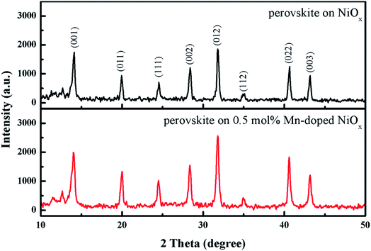 |
| | Fig. 6 XRD patterns of perovskite layers on the un-doped and 0.5 mol% Mn-doped NiOx. | |
Fig. 7(a) displays the steady-state PL spectra of the perovskite layer deposited on the FTO, un-doped and Mn-doped NiOx films with different doping concentration. The decreased PL intensity reveals charge extraction and transport from the perovskite layer to the HTL, which has been extensively discussed in previous literature.27,41 It can be seen that the perovskite cast on the FTO substrate has the highest PL intensity. By casting the perovskite layer on the un-doped NiOx, the PL intensity was significantly lowered due to carrier extraction. By depositing the perovskite on the Mn-doped NiOx, the PL emission was further prohibited, indicative of higher carrier extraction and reduced charge recombination, which bring benefits to short-circuit current density (JSC) and fill factor (FF) of PSCs. The lowest PL emission was observed for the perovskite on the 0.5 mol% Mn-doped NiOx film. To further verify PL results of perovskite films on various substrates, the TR-PL decay technique was applied and the corresponding decay curves are depicted in Fig. 7(b). The PL decay curves are fitted by a biexponential model and the obtained decay constants τ1, τ2, and τavg are summarized in Table S1 in the ESI.† The fast decay constant τ1 represents non-radiative capture of free carriers and the slow decay constant τ2 is associated with radiative recombination of carriers from the bulk perovskite.26,55 The average lifetime (τavg) was determined with the equation τavg = ∑(Aiτi2)/∑(Aiτi), where τi and Ai are deduced from the fitted curve data. The τavg is calculated to be 91, 52.7, 33.1, 37.7, and 51.3 ns for the perovskite films on the FTO, un-doped, 0.5, 1, and 2 mol% Mn-doped NiOx, respectively, which is in accordance with the downtrend of PL emission in Fig. 7(a). It is widely known that the shorter carrier lifetime exhibits more efficient charge extraction. The perovskite film on the 0.5 mol% Mn-doped NiOx owns the most efficient charge extraction among all samples because of the shortest carrier lifetime, indicative of higher device performance of PSCs.
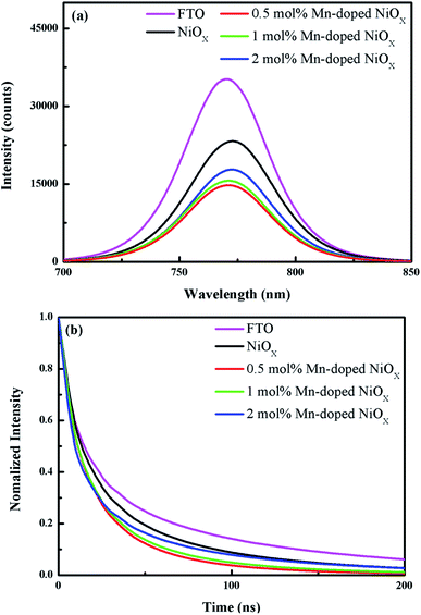 |
| | Fig. 7 (a) PL emission spectra and (b) TR-PL decay curves of the perovskites on the FTO, un-doped and 0.5–2 mol% Mn-doped NiOx. | |
3.3. Device evaluation
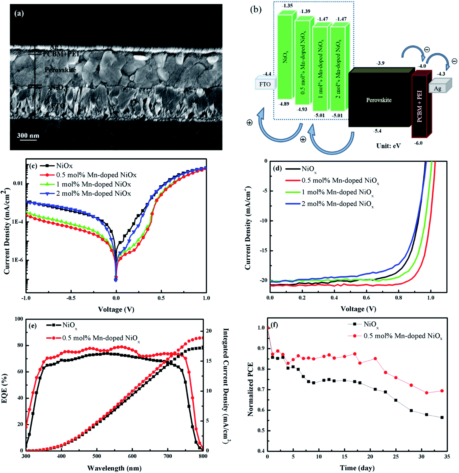
The inverted (p–i–n) PSC with the architecture of FTO/un-doped or Mn-doped NiOx/Cs0.05(MA0.85FA0.15)0.95Pb(Br0.15I0.85)3/PC61BM + TBABF4/PEI/Ag were fabricated and evaluated. The cross-sectional SEM image of the whole device was presented in Fig. 8(a). The thicknesses of the 0.5 mol% Mn-doped NiOx, perovskite, PCBM + TBABF4, PEI, and Ag electrode are estimated to be 30, 550, 40, 20, and 100 nm, respectively. Fig. 8(b) displays the energy level diagram of the whole PSC using the un-doped or Mn-doped NiOx with different concentrations as the HTL. Compared to the pristine NiOx, the 0.5 mol% Mn-doped NiOx has a downward VB at −4.93 eV that matches better with the perovskite layer (VB = −5.4 eV). As mentioned in the UPS part, hole extraction and transport would be improved by reducing energy barrier between the perovskite layer and HTL. To evaluate the charge transport and recombination processes in devices, dark current measurements of PSCs based on the un-doped and Mn-doped NiOx HTLs were carried out and the corresponding dark J–V characteristics are displayed in Fig. 8(c). The 0.5 mol% Mn-doped NiOx device showed the lowest leakage current density among all PSCs under the reverse bias from −1 to 0 V, which is beneficial for improving charge transport and decreasing recombination loss.59 The J–V characteristic curves of all devices using the pristine and Mn-doped NiOx as the HTL under AM 1.5G illumination are depicted in Fig. 8(d). Furthermore, the measured photovoltaic parameters including JSC, open-circuit voltage (VOC), FF, PCE, and series resistance (RS) are listed in Table 1. The control device without Mn doping displayed a moderate PCE of 14.71%, a JSC of 20.74 mA cm−2, a VOC of 0.96 V, and a FF value of 0.73. The best PSC performance was achieved from the device using 0.5 mol% Mn-doped NiOx as the HTL, revealing a PCE of 17.35% which is significantly higher than the control device. The JSC, VOC, and FF of the device were measured to be 20.84 mA cm−2, 1.027 V, and 0.81, respectively. From the literature survey, we realize that our device based on 0.5 mol% Mn-doped NiOx has a prominent PCE which is higher than those devices with other kinds of doping, such as La, Li, or Li–Co–Mg codoping with PCE values in the range of 13.22–15.39%.33,34,38 The introduced amount of Mn dopant in this study is essentially less than other kinds of dopants. Besides, the PSC based on the 1 mol% Mn-doped NiOx showed a PCE of 15.85%, a JSC of 20.08 mA cm−2, a VOC of 1.01 V, and a FF value of 0.78. By further increasing Mn concentration up to 2 mol%, the PCE of the device dropped to 13.82% with a JSC 20.18 mA cm−2, a VOC of 0.97 V, and an FF value of 0.7. To assess reproducibility of our PSCs, the statistical distribution for PCE, VOC, JSC, and FF from 20 individual devices was collected and presented in Fig. S3 in the ESI.† In particular, our devices based on 0.5 mol% Mn-doped NiOx as the HTL revealed the best reproducibility and higher photovoltaic parameters relative to others. As mentioned in the 3.1 section, the hole mobility of NiOx was increased with the Mn-doped amount. However, device performance of PSCs is determined by many factors, not only the hole mobility. From PL and TR-PL decay experiments, we realized that the perovskite deposited on the 0.5 mol% Mn-doped NiOx has the lowest PL intensity and shortest carrier lifetime. From the dark current measurement of devices, the device based on the 0.5 mol% Mn-doped NiOx also has the lowest leakage current density, implying better charge transport and decreased recombination loss. The above factors all contribute to device performance and hence the PSC based on the 0.5 mol% Mn-doped NiOx HTL received the best device parameters. Fig. 8(e) shows the EQE spectra and integrated current densities of devices using the un-doped and 0.5 mol% Mn-doped NiOx as the HTL. The incident photon-to-electron conversion signal as a function of wavelength is observed in a wide range from 300 to 790 nm. The results demonstrate that the EQE of the 0.5 mol% Mn-doped NiOx device was higher than the control one, while the highest EQE value of 80% at around 600 nm was obtained. Besides, we notice that the integrated current density obtained from the EQE spectra (17.16 mA cm−2 for the control device and 18.89 mA cm−2 for the device based on the 0.5 mol% Mn-doped NiOx) are smaller than JSC values. The mismatch between integrated current density and JSC values, originating from different experimental setup, has been reported by Etgar and his coworker.59,60 The J–V measurement of devices is carried out under AM 1.5G irradiation, while the EQE experiment is acquired using Xe lamp as the light source. The acquisition time for EQE experiments is normally longer than that for electrical measurement of devices, and therefore long-term sample degradation may be induced to receive lower integrated current density. The calculated integrated current density less than JSC within 10−20% is reasonably accurate. Dai and his coworkers also claimed that the ion migration by the external bias inside the perovskite films during a relatively long measurement period can result in the decreased integrate current density for the EQE measurement.61 Therefore, the obtained integrated current density that is smaller than JSC within 10–20% is acceptable.60 In this work, the difference between the integrated current density and JSC is found to be 9.4% and 17.3% for devices based on the 0.5 mol% Mn-doped and un-doped NiOx HTLs, respectively, which is believable. To explore environmental stability of PSCs, the fabricated PSCs were exposed to a halogen lamps matrix and their J–V characteristics were measured in each 24 h period.55 Fig. 8(f) shows the PCE evolution of PSCs based on the un-doped and 0.5 mol% Mn-doped NiOx as the HTL, retaining 55% and 70% of initial PCE after 35 days exposure, respectively. It is clearly seen that the PSC based on the 0.5 mol% Mn-doped NiOx HTL possesses higher stability than the control one. The potential mechanism of improved stability of Mn-doped NiOx devices is explained as follows. The SEM and XRD experiments confirm that perovskite layers with larger grains and higher crystallinity can be obtained on the Mn-doped NiOx, as revealed in the 3.2 section. High-quality perovskite absorbers ensure device performance and prevent short-term degradation of devices in the ambient environment. In addition, dark current measurements prove that PSCs based on the Mn-doped NiOx HTL possess a smaller leakage current, especially the 0.5 mol% Mn-doped one. The above results suggest that the Mn-doped NiOx brings better ambient stability of devices compared to the un-doped NiOx. In previous literature, several elements have been doped into NiOx to serve as the HTL in PSCs. Thiruchelvan et al. demonstrated inverted PSCs using Zn-doped NiOx as the HTL, which maintained 80% of their initial efficiency after 108 h (4.5 days) in dark environment at room temperature with 40% relative humidity.35 Choi et al. reported Zn–Ce co-doped NiOx HTL for fabricating PSCs. The device retained 60% of initial efficiency after 120 h (5 days) in ambient environment under 70% relative humidity.36 Bao et al. fabricated PSCs based on Rb-doped NiOx HTL, which aged in the dark at room temperature with 30% relative humidity.61,62 The device retained <70% of initial efficiency after 700 h (29 days) storage. Compare to other doped elements such as K, La, Li, or Li–Co–Mg co-dopant, a smaller amount of the Mn dopant is needed to achieve comparable device performance, and Mn ions would not damage the perovskite layer as released from NiOx lattice. Moreover, our devices using Mn-doped NiOx as the HTL revealed better stability under more severe test condition.
 |
| | Fig. 8 (a) Cross-sectional SEM image, (b) energy level diagram, (c) dark J–V characteristics, and (d) J–V characteristics under AM1.5G illumination of PSCs; (e) EQE spectra and integrated current density of PSCs, and (f) normalized PCE evolution of devices based on the un-doped and 0.5 mol% Mn-doped NiOx as the HTL. | |
Table 1 Device performance of inverted PSCs based on the un-doped and 0.5–2 mol% Mn-doped NiOx as the HTL
| Mn-doped NiOx (mol%) |
Scan direction |
J
SC (mA cm−2) |
V
OC (V) |
FF (%) |
Best PCE (%) |
Avg. PCEa (%) |
R
s (Ω cm2) |
|
An average PCE value was obtained from 20 devices.
|
| 0 |
Forward |
21.19 |
0.94 |
0.64 |
12.84 |
12.28 |
85.33 |
| Reverse |
20.74 |
0.96 |
0.73 |
14.71 |
14.01 |
70.45 |
| 0.5 |
Forward |
21.13 |
1.02 |
0.73 |
15.78 |
14.48 |
54.76 |
| Reverse |
20.84 |
1.027 |
0.81 |
17.35 |
16.23 |
53.07 |
| 1 |
Forward |
20.28 |
0.99 |
0.71 |
14.48 |
14.14 |
74.57 |
| Reverse |
20.08 |
1.01 |
0.78 |
15.85 |
15.04 |
70.71 |
| 2 |
Forward |
20.34 |
0.96 |
0.63 |
12.53 |
12.44 |
100.12 |
| Reverse |
20.18 |
0.97 |
0.70 |
13.82 |
13.49 |
82.32 |
4. Conclusions
In summary, we selected a simple sol–gel process to prepare Mn-doped NiOx layers for enhancing hole extraction and conductivity of the inorganic NiOx HTL. Mn doping can enhance conductivity and charge transport ability of NiOx to bring on JSC enhancement. Higher transmittance of the Mn-doped NiOx HTL in the visible range facilitates incident photons to pass through and to be absorbed by the perovskite layer. The XPS results demonstrate that Mn doping promotes the amount of Ni3+ species and hole transport ability of NiOx. The perovskites on the Mn-doped NiOx have larger grains and higher crystallinity compared with that on the un-doped NiOx, which is beneficial for reducing charge recombination. The reduced PL emission and shortened carrier lifetime of the perovskite on the Mn-doped NiOx demonstrates effective charge extraction. Inverted PSCs base on the Mn-doped NiOx with different doping concentration of 0.5–2 mol% as the HTL were fabricated and evaluated for the first times. The best PSC was achieved using the 0.5 mol% Mn-doped NiOx HTL, revealing the highest PCE of 17.35% and excellent device stability up to 35 days under a continuous halogen lamps matrix exposure in ambient environment. To date, the Mn-doped NiOx is proved to serve as a potential HTL for PSCs with high performance and long-term stability.
Author contributions
Conceptualization: S.-H. Yang; Methodology: Y.-W. Wu and S.-H. Yang; Investigation: Y.-W. Wu, C.-Y. Chang and F.-B. Chiu; Formal Analysis: Y.-W. Wu; Resources: S.-H. Yang; Supervision: S.-H. Yang; Validation: S.-H. Yang; Writing – original draft: Y.-W. Wu; Writing – review and editing: S.-H. Yang. All authors read and approved the final manuscript.
Conflicts of interest
There are no conflicts to declare.
Acknowledgements
The authors thank the Ministry of Science and Technology of the Republic of China under Contract No. MOST 110-2221-E-A49-082-MY3 for financially supporting this work. The authors also gratefully acknowledge the use of SEM (EM000600) belonging to the Core Facility Center of National Cheng Kung University under Contract No. MOST 110-2731-M-006-001.
References
- Y. Chen, H. T. Yi, X. Wu, R. Haroldson, Y. N. Gartstein, Y. I. Rodionov, K. S. Tikhonov, A. Zakhidov, X. Y. Zhu and V. Podzorov, Extended carrier lifetimes and diffusion in hybrid perovskites revealed by Hall effect and photoconductivity measurements, Nat. Commun., 2016, 7, 12253 CrossRef CAS PubMed.
- C. C. Stoumpos, C. D. Malliakas and M. G. Kanatzidis, Semiconducting Tin and Lead Iodide Perovskites with Organic Cations: Phase Transitions, High Mobilities, and Near-Infrared Photoluminescent Properties, Inorg. Chem., 2013, 52, 9019–9038 CrossRef CAS PubMed.
- V. D'Innocenzo, G. Grancini, M. J. P. Alcocer, A. R. S. Kandada, S. D. Stranks, M. M. Lee, G. Lanzani, H. J. Snaith and A. Petrozza, Excitons versus free charges in organo-lead tri-halide perovskites, Nat. Commun., 2014, 5, 3586 CrossRef PubMed.
- S. A. Kulkarni, T. Baikie, P. P. Boix, N. Yantara, N. Mathews and S. Mhaisalkar, Band-gap tuning of lead halide perovskites using a sequential deposition process, J. Mater. Chem. A, 2014, 2, 9221–9225 RSC.
- K. Galkowski, A. Mitioglu, A. Miyata, P. Plochocka, O. Portugall, G. E. Eperon, J. T. W. Wang, T. Stergiopoulos, S. D. Stranks, H. J. Snaith and R. J. Nicholas, Determination of the exciton binding energy and effective masses for methylammonium and formamidinium lead tri-halide perovskite semiconductors, Energy Environ. Sci., 2016, 9, 962–970 RSC.
- A. Kojima, K. Teshima, Y. Shirai and T. Miyasaka, Organometal Halide Perovskites as Visible-Light Sensitizers for Photovoltaic Cells, J. Am. Chem. Soc., 2009, 131, 6050–6051 CrossRef CAS PubMed.
-
National Renewable Energy Laboratory (NREL), Best Research-Cell Efficiency chart, https://www.nrel.gov/pv/cell-efficiency.html, 2022 Search PubMed.
- J. Chen and N. G. Park, Materials and Methods for Interface Engineering toward Stable and Efficient Perovskite Solar Cells, ACS Energy Lett., 2020, 5, 2742–2786 CrossRef CAS.
- I. Hussain, H. P. Tran, J. Jaksik, J. Moore, N. Islam and M. J. Uddin, Functional materials, device architecture, and flexibility of perovskite solar cell, Emerg. Mater., 2018, 1, 133–154 CrossRef CAS.
- P. Zhao, B. J. Kim and H. S. Jung, Passivation in perovskite solar cells: a review, Mater. Today Energy, 2018, 7, 267–286 CrossRef.
- M. Saliba, T. Matsui, K. Domanski, J. Y. Seo, A. Ummadisingu, S. M. Zakeeruddin, J. P. Correa-Baena, W. R. Tress, A. Abate, A. Hagfeldt and M. Grätzel, Incorporation of rubidium cations into perovskite solar cells improves photovoltaic performance, Science, 2016, 354, 206–209 CrossRef CAS PubMed.
- L. A. Frolova, A. I. Davlethanov, N. N. Dremova, I. Zhidkov, A. F. Akbulatov, E. Z. Kurmaev, S. M. Aldoshin, K. J. Stevenson and P. A. Troshin, Efficient and Stable MAPbI3-Based Perovskite Solar Cells Using Polyvinylcarbazole Passivation, J. Phys. Chem. Lett., 2020, 11, 6772–6778 CrossRef CAS PubMed.
- X. Chen, Y. Xia, Z. Zheng, X. Xiao, C. Ling, M. Xia, Y. Hu, A. Mei, R. Cheacharoen, Y. Rong and H. Han, In Situ Formation of δ-FAPbI3 at the Perovskite/Carbon Interface for Enhanced Photovoltage of Printable Mesoscopic Perovskite Solar Cells, Chem. Mater., 2022, 34, 728–735 CrossRef CAS.
- J. W. Lee, D. H. Kim, H. S. Kim, S. W. Seo, S. M. Cho and N. G. Park, Formamidinium and Cesium Hybridization for Photo- and Moisture-Stable Perovskite Solar Cell, Adv. Energy Mater., 2015, 5, 1501310 CrossRef.
- C. Yi, J. Luo, S. Meloni, A. Boziki, N. Ashari-Astani, C. Grätzel, S. M. Zakeeruddin, U. Röthlisberger and M. Grätzel, Entropic stabilization of mixed A-cation ABX3 metal halide perovskites for high performance perovskite solar cells, Energy Environ. Sci., 2016, 9, 656–662 RSC.
- M. Saliba, T. Matsui, J. Y. Seo, K. Domanski, J. P. Correa-Baena, M. K. Nazeeruddin, S. M. Zakeeruddin, W. Tress, A. Abate, A. Hagfeldtd and M. Grätzel, Cesium-containing triple cation perovskite solar cells: improved stability, reproducibility and high efficiency, Energy Environ. Sci., 2016, 9, 1989–1997 RSC.
- L. Meng, J. You, T. F. Guo and Y. Yang, Recent Advances in the Inverted Planar Structure of Perovskite Solar Cells, Acc. Chem. Res., 2016, 49, 155–165 CrossRef CAS PubMed.
- H. A. Dewi, H. Wang, J. Li, M. Thway, R. Sridharan, R. Stangl, F. Lin, A. G. Aberle, N. Mathews, A. Bruno and S. Mhaisalkar, Highly Efficient Semitransparent Perovskite Solar Cells for Four Terminal Perovskite-Silicon Tandems, ACS Appl. Mater. Interfaces, 2019, 11, 34178–34187 CrossRef CAS PubMed.
- A. Guchhait, H. A. Dewi, S. W. Leow, H. Wang, G. Han, F. B. Suhaimi, S. Mhaisalkar, L. H. Wong and N. Mathews, Over 20% Efficient CIGS−Perovskite Tandem Solar Cells, ACS Energy Lett., 2017, 2, 807–812 CrossRef CAS.
- H. Li and W. Zhang, Perovskite Tandem Solar Cells: From Fundamentals to Commercial Deployment, Chem. Rev., 2020, 120, 9835–9950 CrossRef CAS PubMed.
- Z. Xiao, C. Bi, Y. Shao, Q. Dong, Q. Wang, Y. Yuan, C. Wang, Y. Gao and J. Huang, Efficient, high yield perovskite photovoltaic devices grown by interdiffusion of solution-processed precursor stacking layers, Energy Environ. Sci., 2014, 7, 2619–2623 RSC.
- W. Nie, H. Tsai, R. Asadpour, J. C. Blancon, A. J. Neukirch, G. Gupta, J. J. Crochet, M. Chhowalla, S. Tretiak, M. A. Alam, H. L. Wang and A. D. Mohite, High-efficiency solution-processed perovskite solar cells with millimeter-scale grains, Science, 2015, 347, 522–525 CrossRef CAS PubMed.
- M. D. Irwin, D. B. Buchholz, A. W. Hains, R. P. H. Chang and T. J. Marks, p-Type semiconducting nickel oxide as an efficiency-enhancing anode interfacial layer in polymer bulk-heterojunction solar cells, Proc. Natl. Acad. Sci. U. S. A., 2008, 105, 2783–2787 CrossRef CAS.
- D. Zhao, M. Sexton, H. Y. Park, G. Baure, J. C. Nino and F. So, High-Efficiency Solution-Processed Planar Perovskite Solar Cells with a Polymer Hole Transport Layer, Adv. Energy Mater., 2014, 5, 1401855 CrossRef.
- P. S. Patil and L. D. Kadam, Preparation and characterization of spray pyrolyzed nickel oxide (NiO) thin films, Appl. Surf. Sci., 2002, 199, 211–221 CrossRef CAS.
- L. Huang, Y. Wang, X. Zhu, X. Zhao, G. Li, L. Li and W. Sun, Mg-Doped Nickel Oxide as Efficient Hole-Transport Layer for Perovskite Photodetectors, J. Phys. Chem. C, 2021, 125, 16066–16074 CrossRef CAS.
- L. Hu, J. Peng, W. Wang, Z. Xia, J. Yuan, J. Lu, X. Huang, W. Ma, H. Song, W. Chen, Y. B. Cheng and J. Tang, Sequential Deposition of CH3NH3PbI3 on Planar NiO Film for Efficient Planar Perovskite Solar Cells, ACS Photonics, 2014, 1, 547–553 CrossRef CAS.
- M. Utriainen, M. Kröger-Laukkanen and L. Niinistö, Studies of NiO thin film formation by atomic layer epitaxy, Mater. Sci. Eng. B, 1998, 54, 98–103 CrossRef.
- Y. Xie, W. Wang, Y. Qian, L. Yang and Z. Chen, Deposition and microstructural characterization of NiO thin films by a spray pyrolysis method, J. Cryst. Growth, 1996, 167, 656–659 CrossRef.
- H. Zhang, J. Cheng, F. Lin, H. He, J. Mao, K. S. Wong, A. K. Y. Jen and W. C. H. Choy, Pinhole-Free and Surface-Nanostructured NiOx Film by Room-Temperature Solution Process for High-Performance Flexible Perovskite Solar Cells with Good Stability and Reproducibility, ACS Nano, 2016, 10, 1503–1511 CrossRef CAS PubMed.
- E. Thimsen, A. B. F. Martinson, J. W. Elam and M. J. Pellin, Energy Levels, Electronic Properties, and Rectification in Ultrathin p-NiO Films Synthesized by Atomic Layer Deposition, J. Phys. Chem. C, 2012, 116, 16830–16840 CrossRef CAS.
- A. Corani, M. H. Li, P. S. Shen, P. Chen, T. F. Guo, A. E. Nahhas, K. Zheng, A. Yartsev, V. Sundström and C. S. Ponseca Jr, Ultrafast Dynamics of Hole Injection and Recombination in Organometal Halide Perovskite Using Nickel Oxide as p-Type Contact Electrode, J. Phys. Chem. Lett., 2016, 7, 1096–1101 CrossRef CAS PubMed.
- S. Teo, Z. Guo, Z. Xu, C. Zhang, Y. Kamata, S. Hayase and T. Ma, The Role of Lanthanum in a Nickel Oxide-Based Inverted Perovskite Solar Cell for Efficiency and Stability Improvement, ChemSusChem, 2019, 12, 518–526 CrossRef CAS PubMed.
- M. A. Park, I. J. Park, S. Park, J. Kim, W. Jo, H. J. Son and J. Y. Kim, Enhanced electrical properties of Li-doped NiOx hole extraction layer in p-i-n type perovskite solar cells, Curr. Appl. Phys., 2018, 18, S55–S59 CrossRef.
- P. S. Thiruchelvan, C. C. Lai and C. H. Tsai, Combustion Processed Nickel Oxide and Zinc Doped Nickel Oxide Thin Films as a Hole Transport Layer for Perovskite Solar Cells, Coatings, 2021, 11, 627 CrossRef CAS.
- F. P. G. Ghoi, H. M. Alishah and S. Gunes, Cerium and zinc co-doped nickel oxide hole transport layers for gamma-butyrolactone based ambient air fabrication of CH3NH3PbI3 perovskite solar cells, Appl. Surf. Sci., 2021, 563, 150249 CrossRef.
- S. Wang, B. Zhang, D. Feng, Z. Lin, J. Zhang, Y. Hao, X. Fan and J. Chang, Achieving high performance and stable inverted planar perovskite solar cells using lithium and cobalt co-doped nickel oxide as hole transport layers, J. Mater. Chem. C, 2019, 7, 9270–9277 RSC.
- F. P. G. Choi, H. M. Alishah, S. Bozar, C. Kahveci, M. C. Rodop and S. Gunes, First demonstration of lithium, cobalt and magnesium introduced nickel oxide hole transporters for inverted methylammonium lead triiodide based perovskite solar cells, Sol. Energy, 2021, 215, 434–442 CrossRef.
- W. Liu, L. Chu, N. Liu, Y. Ma, R. Hu, Y. Weng, H. Li, J. Zhang, X. Li and W. Huang, Efficient perovskite solar cells fabricated by manganese cations incorporated in hybrid perovskites, J. Mater. Chem. C, 2019, 7, 11943–11952 RSC.
- W. Zhou, S. Chen, Y. Zhao, Q. Li, Y. Zhao, R. Fu, D. Yu, P. Gao and Q. Zhao, Constructing CsPbBr3 Cluster Passivated-Triple Cation Perovskite for Highly Efficient and Operationally Stable Solar Cells, Adv. Funct. Mater., 2019, 29, 1809180 CrossRef.
- S. Xiong, M. Yuan, J. Yang, J. Song, X. Guo, X. Li, B. Li, X. Liu, C. Duan, F. Liu, M. Fahlaman and Q. Bao, Engineering of the Back Contact between PCBM and Metal Electrode for Planar Perovskite Solar Cells with Enhanced Efficiency and Stability, Adv. Opt. Mater., 2019, 7, 1900542 CrossRef CAS.
- X. Wang, A. Tang, F. Chen and E. Zhou, The effect of conjugated π-bridge and fluorination on the properties of asymmetric-building-block-containing polymers (ABC polymers) based on dithienopyran donor and benzothiadiazole acceptors, Polym. Chem., 2017, 8, 5396–5406 RSC.
- G. Boschloo and A. Hagfeldt, Spectroelectrochemistry of Nanostructured NiO, J. Phys. Chem. B, 2001, 105, 3039–3044 CrossRef CAS.
- Z. Wang, J. Lin, H. Xu, Y. Zheng, Y. Xiao and Y. Zheng, Zr-Doped NiO Nanoparticles for Low-Temperature Methane Combustion, ACS Appl. Nano Mater., 2021, 4, 11920–11930 CrossRef CAS.
- J. S. Valente, M. Valle-Orta, H. Armendáriz-Herrera, R. Quintana-Solórzano, P. del Angel, J. Ramírez-Salgado and J. R. Montiel-López, Controlling the redox properties of nickel in NiOx/ZrO2 catalysts synthesized by sol–gel, Catal. Sci. Technol., 2018, 8, 4070–4082 RSC.
- W. Chen, F. Z. Liu, X. Y. Feng, A. B. Djurišić, W. K. Chan and Z. B. He, Cesium Doped NiOx as an Efficient Hole Extraction Layer for Inverted Planar Perovskite Solar Cells, Adv. Energy Mater., 2017, 7, 1700722 CrossRef.
- M. Yang, H. Pu, Q. Zhou and Q. Zhang, Transparent p-type conducting K-doped NiO films deposited by pulsed plasma deposition, Thin Solid Films, 2012, 520, 5884–5888 CrossRef CAS.
- X. Wan, Y. Jiang, Z. Qiu, H. Zhang, X. Zhu, I. Sikandar, X. Liu, X. Chen and B. Cao, Zinc as a New Dopant for NiOx-Based Planar Perovskite Solar Cells with Stable Efficiency near 20%, ACS Appl. Energy Mater., 2018, 1, 3947–3954 CrossRef CAS.
- Z. W. Huang, S. H. Yang, Z. Y. Wu and H. C. Hsu, Performance Comparison between the Nanoporous NiOx Layer and NiOx Thin Film for Inverted Perovskite Solar Cells with Long-Term Stability, ACS Omega, 2021, 6, 15855–15866 CrossRef CAS PubMed.
- G. Shen, Q. Cai, H. Dong, X. Wen, X. Xu and C. Mu, Using Interfacial Contact Engineering to Solve Nickel Oxide/Perovskite Interface Contact Issues in Inverted Perovskite Solar Cells, ACS Sustain. Chem. Eng., 2021, 9, 3580–3589 CrossRef CAS.
- R. Azmi, V. Trouillet, M. Strafela, S. Ulrich, H. Ehrenberg and M. Bruns, Surface analytical approaches to reliably characterize lithium ion battery electrodes, Surf. Interface Anal., 2018, 50, 43–51 CrossRef CAS.
- J. He, M. Wang, W. Wang, R. Miao, W. Zhong, S. Y. Chen, S. Poges, T. Jafari, W. Song, J. Liu and S. L. Suib, Hierarchical Mesoporous NiO/MnO2@PANI Core−Shell Microspheres, Highly Efficient and Stable Bifunctional Electrocatalysts for Oxygen Evolution and Reduction Reactions, ACS Appl. Mater. Interfaces, 2017, 9, 42676–42687 CrossRef CAS PubMed.
- M. A. Afroz, R. Garai, R. K. Gupta and P. K. Iyer, Additive-Assisted Defect Passivation for Minimization of Open-Circuit Voltage Loss and Improved Perovskite Solar Cell Performance, ACS Appl. Energy Mater., 2021, 4, 10468–10476 CrossRef CAS.
- P. Chen, Y. Bai, S. Wang, M. Lyu, J. H. Yun and L. Wang, In Situ Growth of 2D Perovskite Capping Layer for Stable and Efficient Perovskite Solar Cells, Adv. Funct. Mater., 2018, 28, 1706923 CrossRef.
- B. R. Jheng, P. T. Chiu, S. H. Yang and Y. L. Tong, Using ZnCo2O4 nanoparticles as the hole transport layer to improve long term stability of perovskite solar cells, Sci. Rep., 2022, 12, 2921 CrossRef CAS PubMed.
- J. Zheng, L. Hu, J. S. Yun, M. Zhang, C. F. J. Lau, J. Bing, X. Deng, Q. Ma, Y. Cho, W. Fu, C. Chen, M. A. Green, S. Huang and A. W. Y. Ho-Baillie, Solution-Processed, Silver-Doped NiOx as Hole Transporting Layer for High-Efficiency Inverted Perovskite Solar Cells, ACS Appl. Energy Mater., 2018, 1, 561–570 CrossRef CAS.
- T. Wang, Z. Cheng, Y. Zhou, H. Liu and W. Shen, Highly efficient and stable perovskite solar cells via bilateral passivation layers, J. Mater. Chem. A, 2019, 7, 21730–21739 RSC.
- G. Zheng, C. Zhu, J. Ma, X. Zhang, G. Tang, R. Li, Y. Chen, L. Li, J. Hu, J. Hong, Q. Chen, X. Gao and H. Zhou, Manipulation of facet orientation in hybrid perovskite polycrystalline films by cation cascade, Nat. Commun., 2018, 9, 2793 CrossRef PubMed.
- W. Ke, C. C. Stoumpos, I. Spanopoulos, M. Chen, M. R. Wasielewski and M. G. Kanatzidis, Diammonium Cations in the FASnI3 Perovskite Structure Lead to Lower Dark Currents and More Efficient Solar Cells, ACS Energy Lett., 2018, 3, 1470–1476 CrossRef CAS.
- M. Saliba and L. Etgar, Current Density Mismatch in Perovskite Solar Cells, ACS Energy Lett., 2020, 5, 2886–2888 CrossRef CAS.
- Y. Qi, D. Ndaleh, W. E. Meador, J. H. Delcamp, G. Hill, N. R. Pradhan and Q. Dai, Interface Passivation of Inverted Perovskite Solar Cells by Dye Molecules, ACS Appl. Energy Mater., 2021, 4, 9525–9533 CrossRef CAS.
- H. Bao, M. Du, H. Wang, K. Wang, X. Zuo, F. Liu, L. Liu, D. Eder, A. Cherevan, S. Wang, L. Wan, S. Zhao and S. F. Liu, Samarium-Doped Nickel Oxide for Superior Inverted Perovskite Solar Cells: Insight into Doping Effect for Electronic Applications, Adv. Funct. Mater., 2021, 31, 2102452 CrossRef CAS.
|
| This journal is © The Royal Society of Chemistry 2022 |
Click here to see how this site uses Cookies. View our privacy policy here. 
 Open Access Article
 This Open Access Article is licensed under a Creative Commons Attribution-Non Commercial 3.0 Unported Licence
 *
*