
 Open Access Article
 This Open Access Article is licensed under a Creative Commons Attribution-Non Commercial 3.0 Unported Licence
Preparation and defect structure analysis of near-stoichiometric lithium tantalate wafers
Xuefeng Xiao†
 *abc,
Qingyan Xu†abc,
Shuaijie Liangabc,
Huan Zhangab,
Lingling Maab,
Lian Haiab and
Xuefeng Zhangc
*abc,
Qingyan Xu†abc,
Shuaijie Liangabc,
Huan Zhangab,
Lingling Maab,
Lian Haiab and
Xuefeng Zhangc
aCollege of Electric and Information Engineering, North Minzu University, Yinchuan, China. E-mail: xxf666666@163.com
bKey Laboratory of Physics and Photoelectric Information Functional Materials Sciences and Technology, North Minzu University, Yinchuan, China
cNingxia Ju Jing Yuan Crystal Technology Company Limited, Shizuishan, China
First published on 30th June 2022
Abstract
A vapour transfer equilibrium (VTE) method has been used to prepare near-stoichiometric lithium tantalate (NSLT) crystals with different Li contents. The NSLT crystals were tested and analyzed by differential thermal analysis (DTA) and X-ray photoelectron spectroscopy (XPS) to investigate the effect of Li content on the Curie temperature and internal defects of NSLT crystals. This study found that when the Li content increased in the NSLT wafer, the binding energy corresponding to the peak of the Ta4f electron layer in the XPS spectrum first decreased and then increased, indicating that the proportion of Ta valence states was different in wafers with different Li contents. From XPS energy spectrum analysis, it can be seen that the lithium tantalate crystal contains Ta5+, Ta4+, Ta3+ and lower-valence Ta. As the Li content increases in the NSLT wafer, Ta4+ disappears and the proportion of Ta5+ decreases initially, follows by a later increase and then subsequent further decrease. However, the change in proportion of Ta3+ and lower-price Ta is completely opposite to that of Ta5+, showing a trend of first rising, then falling and then finally rising again. Moreover, when the Li content is 49.751% in the NSLT wafer, the proportion of Ta5+ reaches a maximum, showing that at this Li concentration the NSLT crystal has a more perfect lattice structure. In this study, we propose a mixed defect model in which polarons coexist with Li vacancies and Ta inversion, explaining the change in Ta valence state in lithium tantalate crystals. This model is more in line with the observed results in this work. The new hybrid defect model and the variation law of Ta valence state with Li concentration proposed in this paper provide a new direction and experimental proof for the defect study of NSLT crystals, and also provide a theoretical basis to explore the Li content at the best physical properties of NSLT crystals.
1 Introduction
Lithium tantalate (LiTaO3,LT) crystal is an excellent piezoelectric, ferroelectric and optical crystal with good piezoelectric, pyroelectric and electro-optical properties.1,2 It can be used to make filters, lasers, oscillators and other devices, and is known as the “universal crystal”. LT crystals are also known as the most important basic material for wireless communication because of their unique advantages in making SAW filters.3 In addition, LT crystals have important applications not only in acoustics but also in optics, especially in lidar, air pollution detection and medical examination. At present, there are many studies on the optical application of NSLT crystals, including the application of NSLT crystals in lasers when doped with other ions.4–8The crystals are divided into congruent lithium tantalate (CLT) and near-stoichiometric lithium tantalate (NSLT) crystals, according to the Li-to-Ta ratio in LT crystals. Among these, the ratio of Li and Ta in CLT crystals is approximately 48.5![[thin space (1/6-em)]](https://www.rsc.org/images/entities/char_2009.gif) :51.5, while the ratio of Li and Ta in NSLT crystals is close to 1:1. Due to the reduced Li content in CLT, a large number of defects appear in the crystal,9 including Li vacancies (VLi)10 and Ta inversion defects (Ta in Li position, TaLi).11 Li vacancy defects will increase the coercivity field inside the crystal12 and TaLi defects cause optical damage.13 Therefore, Li content has a great influence on the internal defect structure and crystal properties of LT, as the internal defects of LT crystals affect the crystal lattice and conductive carriers.14,15 Therefore, the Li concentration in LT crystals has an impact on the thermal conductivity and conductivity of the crystal and, thus, on the performance of the device.
:51.5, while the ratio of Li and Ta in NSLT crystals is close to 1:1. Due to the reduced Li content in CLT, a large number of defects appear in the crystal,9 including Li vacancies (VLi)10 and Ta inversion defects (Ta in Li position, TaLi).11 Li vacancy defects will increase the coercivity field inside the crystal12 and TaLi defects cause optical damage.13 Therefore, Li content has a great influence on the internal defect structure and crystal properties of LT, as the internal defects of LT crystals affect the crystal lattice and conductive carriers.14,15 Therefore, the Li concentration in LT crystals has an impact on the thermal conductivity and conductivity of the crystal and, thus, on the performance of the device.
The crystal structures of LT and lithium niobate (LN) crystals are similar, so the defect structure of LN crystals is investigated in this paper. Initially, Lerner et al. proposed the most widely-used defect model, the Nb anti-occupancy defect model.16 Later, Kim et al. perfected the model, proposing that the anti-occupied Nb is surrounded by three Li vacancies and one Li vacancy along the c-axis.17 More recently, Chen et al. used density functional theory, X-ray diffraction (XRD) and high-temperature Raman spectroscopy to study the defects of LN and near-stoichiometric lithium niobate (NSLN) crystals.18 It was found that Nb in Li positions (NbLi) and VLi defects are the most stable defects in LN crystals, further proving the applicability of NbLi and VLi defects.
Leroux et al. used high-resolution electron microscopy to study the defects of LN crystals and found many 1 nm defects.19 Based on this phenomenon, a Nb2O5 cluster defect model was proposed. Among these clusters, the cation arrangement along the c-axis changes from normal -LiNb-□-LiNb-□- to ilmenite stacking -LiNb-□-NbLi-□-. Maaider K et al. found a characteristic peak of 738 cm−1 in the Raman spectrum of LN, which is characteristic of titanite.20 Therefore, it was concluded that the defect structure of LN crystal is suitable for modelling using the Nb2O5 cluster defect model.
Although VNb (Nb vacancies) cannot exist from the energy point of view, Abdi et al. verified the possibility of coexistence of VLi with VNb using Raman spectroscopy, with VLi dominating.21 Meanwhile, the study of LN crystal spectra revealed the presence of polaritons in LN crystals.22 Shi et al. studied the defect structure of LN using high-temperature optical reduction spectroscopy, and concluded that LN crystal contains not only free polarons (quasiparticles composed of trapped electrons and local distortion), but also bound polarons and bipolarons.23 Diffraction density tests also support the existence of polarons, and NbLi absorbs electrons more easily than NbNb.24 Schmidt et al. calculated various defect models of near-stoichiometric lithium niobate crystals using density functional theory (DFT), and found that the NbLi4+ defect is equivalent to an NbV + VLi defect.25 Moreover, O and Nb in LN crystals can capture excess electrons to form polarons.
At present, there are three defect models of LN. The most applicable and accepted models are the VLi + NbLi defect model, the Nb2O5 cluster defect model, and the model based on the NbLi + VLi defect model with the addition of polaritons.16–25 Since the structure of LT crystals is similar to that of LN crystals, the defect model of LT crystals is considered to be the same as that of LN crystals, which also conforms to the above three defect models.
In this work, NSLT wafers with different Li concentrations were prepared using a VTE method. The effects of Curie temperature and internal Li content on the atomic valence of NSLT crystals were studied. The binding energies and valence change law of Ta and O were studied by XPS. The change law of internal defects in NSLT crystals with changing Li concentration was obtained, and the defect model was verified experimentally as being in line with the change law of NSLT defects.
2 Experiment
2.1 Preparation of NSLT wafer
Lithium carbonate (Li2CO3) and tantalum oxide (Ta2O5) were fully mixed with a roller ball mill in a fixed molar ratio, and the LT polycrystalline material was made by holding at 1300 °C for 6 h in a high-temperature furnace. The polycrystalline material was placed in a ceramic crucible and grown by a pulling method. The grown crystal was processed by grinding, slicing, grinding and polishing to make the LT wafer.Li2CO3 (99.99%) and Ta2O5 (99.99%) were mixed according to a certain molar ratio, and then mixed evenly and kept at a high temperature for a period of time as standby diffusion material. Then, the LT wafer and diffusion material were alternately placed into the ceramic crucible and heated in the high-temperature furnace to make the NSLT wafer. NSLT wafers processed by VTE were labelled as #1 and NSLT wafers processed by VTE were numbered as #2, #3 and #4. All chips were Y36° LT chips. As shown in Fig. 1, #1 chips are light yellow, while #2, #3 and #4 chips are white. Wafer #1 was an untreated LT wafer, wafer #2 was insulated in the diffusion material at 1300 °C for 60 h, wafer #3 was insulated in the diffusion material at 1250 °C for 60 h, and #4 wafer was insulated in the diffusion material at 1160 °C for 60 h.
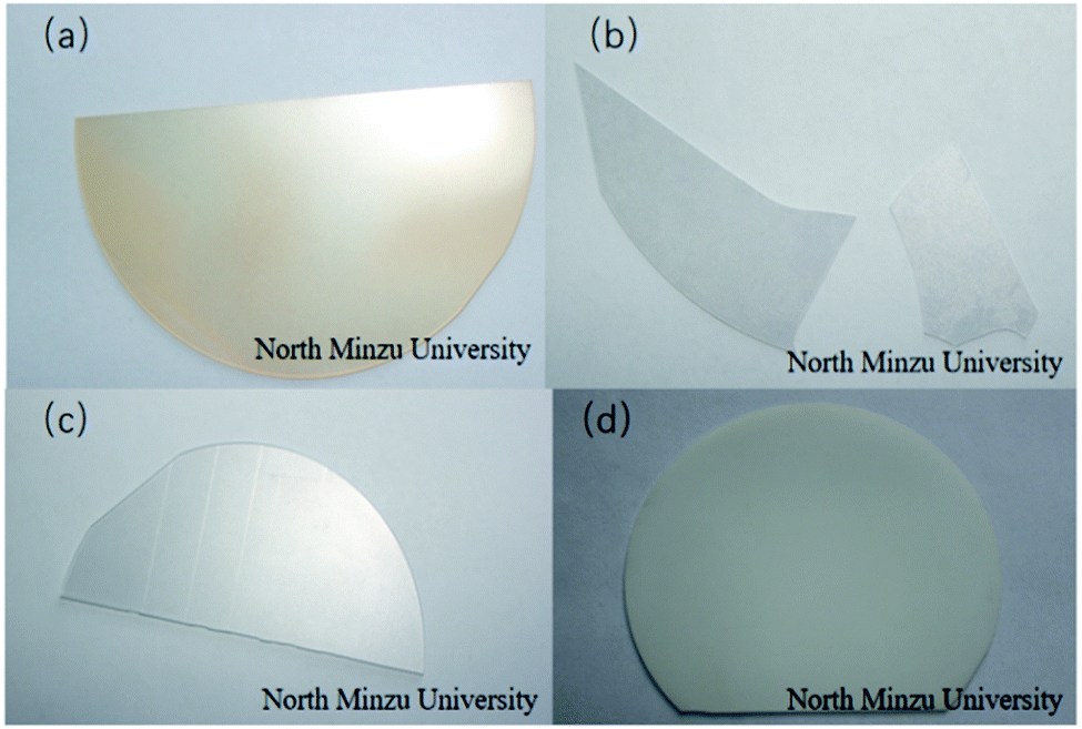 | ||
| Fig. 1 LT wafers (a) #1 (b) #2 (c) #3 (d) #4. | ||
2.2 Differential thermal analysis (DTA) testing
Testing was performed using a Shimadzu DTG-60AH differential thermal analyser (DTA) with N2 as a pure protective gas. The heating rate was 20°C min−1 from room temperature to 800 °C. The argon flow rate was 50 mL min−1. Samples #1, #2, #3 and #4 were all tested under the same conditions.2.3 X-ray photoelectron spectroscopy (XPS) testing
The XPS spectra of all LT samples were measured using a ThermoFisher Scientific k-Alpha X-ray photoelectron spectrometer. Each test sample was etched twice. The XPS spectra of the sample surface, with etching depths of 40 and 80 nm were both tested. All samples were tested under the same conditions.2.4 Raman spectrum testing
The Raman spectra of the LT and NSLT crystal samples were tested using an inViaTM laser confocal micro Raman spectrometer from Renishaw, UK. A 532 nm laser with an exposure time of 10 s was used and scanned in the range of 100–1000 cm−1. All samples were tested under the same conditions.2.5 Raman imaging testing
An array of 4800 Raman spectra was sequentially acquired at 1 μm step intervals in the selected 60 μm × 80 μm region for Raman imaging of the target peaks. The 4800 acquired Raman spectra were subjected to uniform cosmic ray removal and the imaging peaks were fitted using analytical software, and then microscopic Raman imaging was performed using the peak positions of the fitted spectral peaks. All samples were tested under the same conditions.3 Results and discussion
3.1 Differential thermal analysis
After a series of processes of cleaning, drying and grinding, the NSLT wafers with different Li contents were made into powder samples for DTA. The sample mass is shown in Table 1. When the test sample changes phase, the LT powder goes through an endothermic process; that is, when the LT sample changes from ferromagnetic to paramagnetic, there will be a step-wise shape first, and then a clear inflection point. At this time, the transformation of the LT sample from ferromagnetic to paramagnetic will first appear as a step, and then an obvious inflection point, which corresponds to the Curie temperature of the LT wafer.26 It can be seen from Fig. 2 that the Curie temperatures of #1, #2, #3 and #4 samples are 604.06, 648.6, 677.23 and 691.01 °C, respectively. The LT wafers treated using the VTE method have higher Curie temperatures than the untreated LT wafer. The Curie temperature may reflect the lithium content inside the LT wafer. According to Yang et al.,27 the formula relating Curie temperature and lithium content is as follows:| Tc = −2821.1 + 70.3143CLi | (1) |
| CLi = 40.121 + 1.422 × 10⁻² Tc | (2) |
| Sample number | #1 | #2 | #3 | #4 |
|---|---|---|---|---|
| Quality (mg) | 16.57 | 26.59 | 31.54 | 31.90 |
| Curie temperature (°C) | 604.06 | 648.60 | 677.23 | 691.01 |
| Li content (%) | 48.710 | 49.344 | 49.751 | 49.947 |
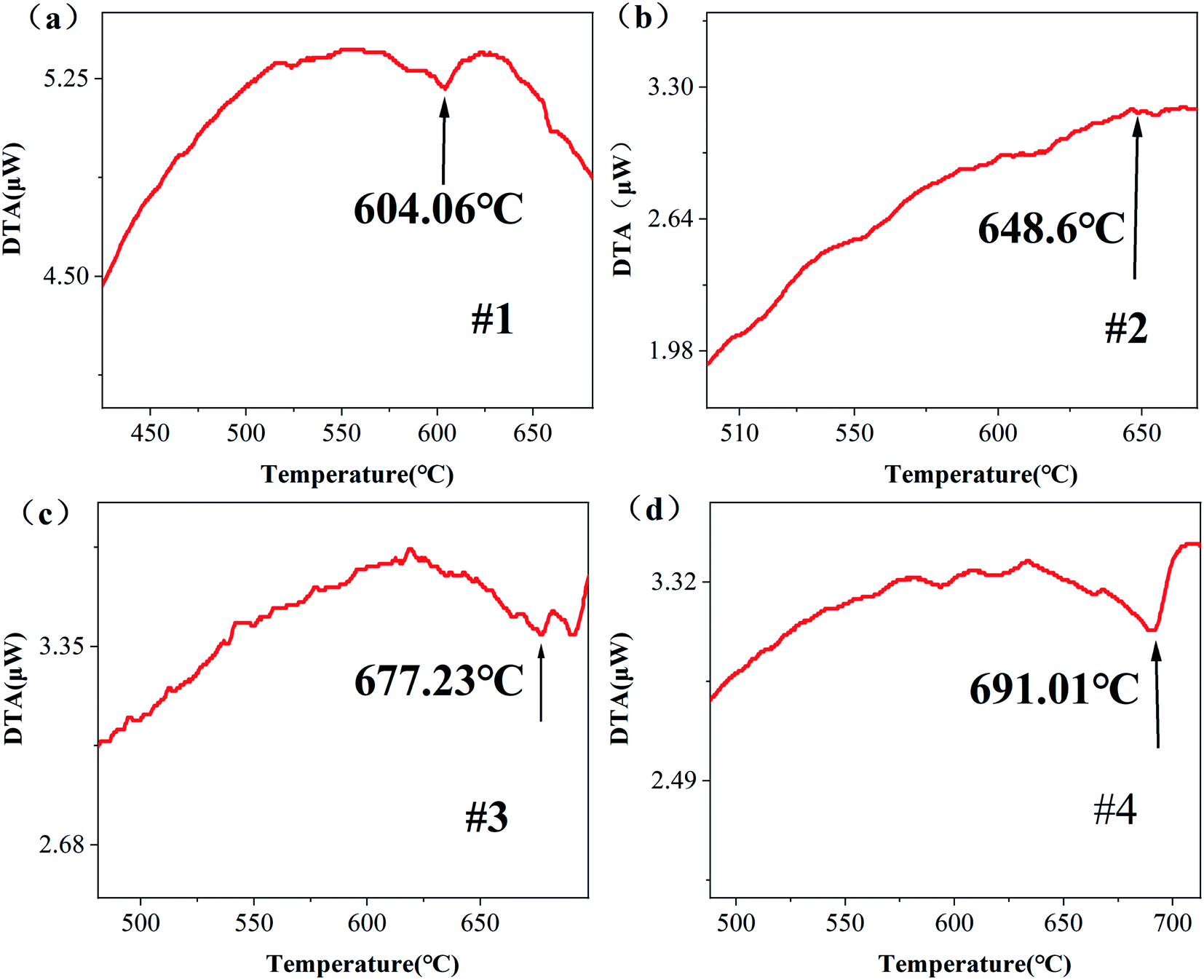 | ||
| Fig. 2 DTA diagram of wafers (a) #1 (b) #2 (c) #3 (d) #4. | ||
According to the above formula, the Li concentration of samples #1–3 and #4 is 48.710%, 49.344%, 49.750% and 49.947%, respectively. From the calculated Li concentrations, it can be seen that chip #1 is the CLT chip, and the Li/Ta of sample #4 is the closest to 1:1.
3.2 X-ray photoelectron spectroscopy (XPS) analysis
It can be seen from Table 2 that the O content on the surface of samples #1–4 is 57.11%, 50.81%, 50.06% and 49.57%, respectively, showing that the O atomic content on the surface of crystals #2–4 crystals is less than that of #1. When the etching depth is 40 or 80 nm, samples #1–4 show little difference in O atomic content. Therefore, the use of the VTE method causes the surface of the wafer to lose a small amount of O atoms at high temperatures. However, this will not have a great impact on the internal O atomic content. The relative atomic proportion of O decreases in the wafer, thus, the relative Li content of VTE-treated LT crystals increases.| O Atomic (%) | Sample number | |||
|---|---|---|---|---|
| #1 | #2 | #3 | #4 | |
| Surface | 57.11 | 50.81 | 50.06 | 49.57 |
| Etching depth 40 nm | 46.70 | 49.26 | 48.12 | 47.70 |
| Etching depth 80 nm | 47.29 | 44.21 | 46.19 | 46.75 |
| Average | 50.40 | 48.09 | 48.12 | 48.00 |
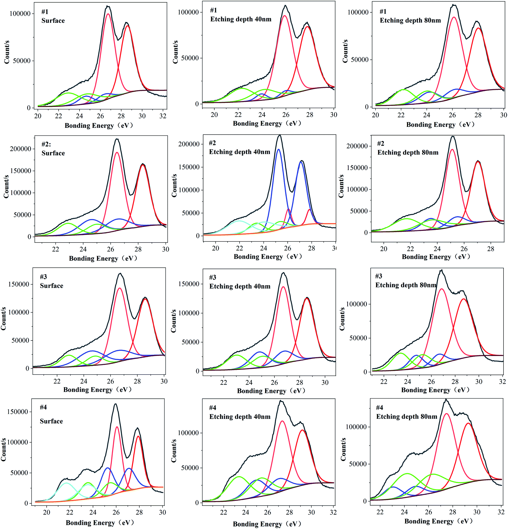
Fig. 3 is the XPS energy spectrum of the Ta4f electron layer at different depths for each sample. It can be seen from Fig. 3 that the peak binding energy of Ta4f electron layer in samples #1, #3 and #4 is higher than that of the surface, and the peak binding energy of Ta4f electron layer on sample #2's surface is equal to that of the inner layer. The valence state of Ta is related to the binding energy of Ta4f electron layer. According to this analysis, it can be concluded that the valence states of Ta in the surface and inner layer for samples #1, #3 and #4 are different, and for sample 2 they are the same. Table 3 and Fig. 4 show the corresponding binding energy values and comparison diagrams of Ta4f electron layer peaks of samples #1–4. It is clear that the double peak binding energy of the Ta4f electron layer of samples #3 and #4 is higher than that of samples #1 and #2. The double peak binding energy of Ta4f in sample #2 is the lowest among the four samples, i.e., with increasing Li the peak binding energy of the Ta4f electron layer first decreases and then increases.
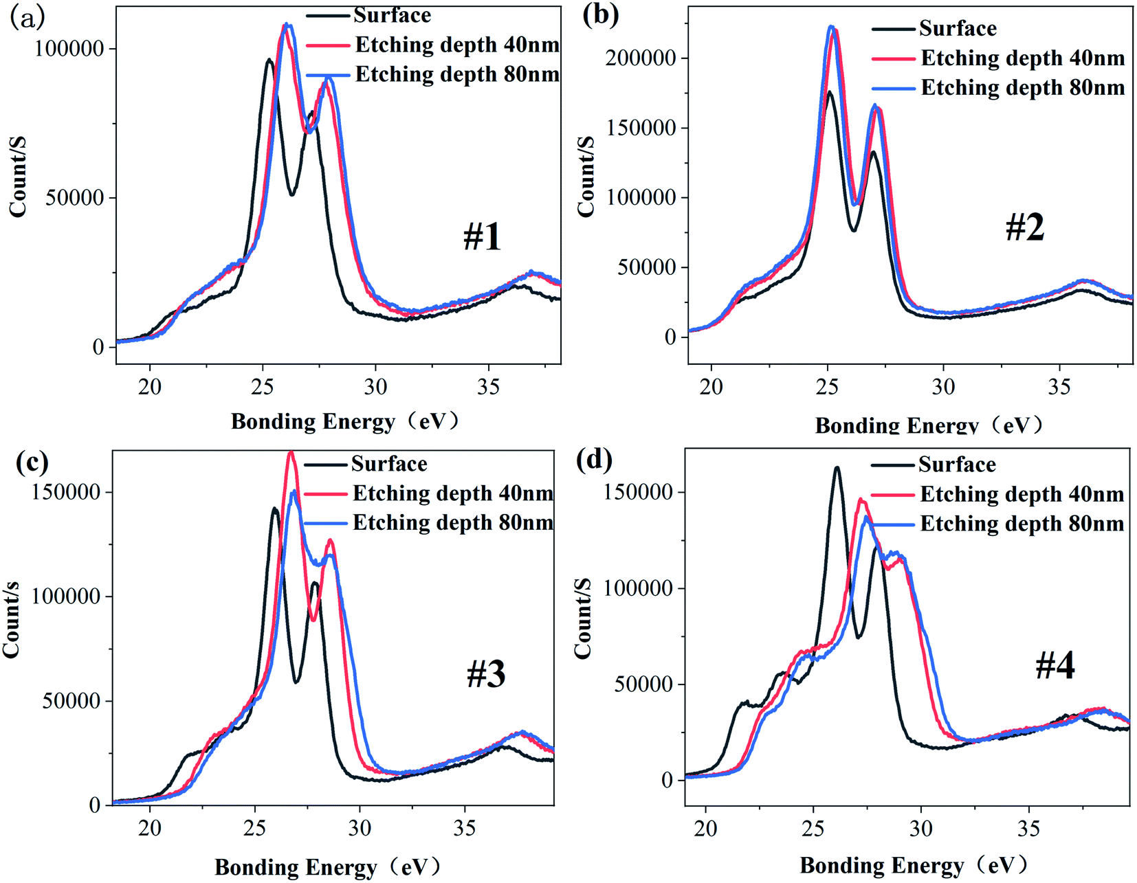 | ||
| Fig. 3 XPS spectra of Ta4F electron layer on the surface and etching depth of 40 nm and 80 nm (a) #1 (b) #2 (c) #3 (d) #4. | ||
| Etching depth (nm) | 0 | 40 | 80 | |||
|---|---|---|---|---|---|---|
| #1 peak binding energy (eV) | 25.28 | 27.18 | 25.93 | 27.78 | 26.03 | 27.83 |
| #2 peak binding energy (eV) | 25.08 | 26.98 | 25.33 | 27.18 | 25.13 | 27.03 |
| #3 peak binding energy (eV) | 25.93 | 27.83 | 26.73 | 28.58 | 26.88 | 28.58 |
| #4 peak binding energy (eV) | 26.08 | 27.98 | 27.18 | 28.98 | 27.43 | 28.58 |
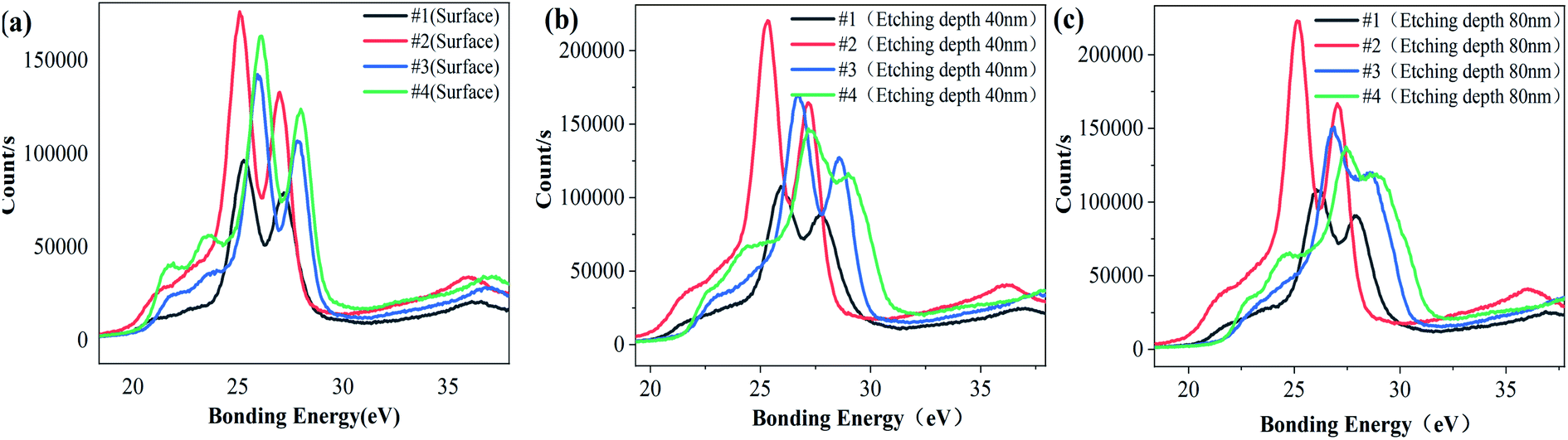 | ||
| Fig. 4 Comparison of XPS spectra of Ta4F electronic layer with the same depth (a) surface (b) etching depth of 40 nm (c) etching depth of 80 nm. | ||
The XPS spectrum was fitted using Thermo Avantage software. Using a Shirley background, a peak width less than 2.7 eV, and bimodal fitting, the area ratio of Ta4f7/2 to Ta4f5/2 is calculated as 4:3, and the peak spacing between Ta4f7/2 and Ta4f5/2 is 1.8–2.1 eV.28 From the paper of Sun De-hui, we obtained that the binding energy of Ta4f7/2 (corresponding to Ta5+) is 27.6 eV, and the binding energy of Ta4f7/2 (corresponding to TaLi4+) is 25.6 eV.29 When Ta is in the environment of oxygen atoms, the binding energies are 26.05 eV for Ta5+, 24.5–24.7 eV for the binding energy of Ta4+/Ta3+, and 23.1–23.3 for Ta2+.28 From the NIST XPS database, the binding energy of the Ta4f7/2 electron layer of Ta4C3 is 23.11 eV.30 From analysis of the above results, we consider that the binding energy of Ta5+ is greater than 26.05 eV, the binding energy of Ta4+ is between 25.4–26.05 eV, the binding energy of Ta3+ is 23.11–25.4 eV, and the lower valence Ta ion has binding energy lower than 23.11 eV.
Fig. 5 shows the fitting of the electron peaks of the Ta4f layer. From the fitting of the binding energy corresponding to the double peak, LT crystals contain Ta not only as Ta5+, but also in other valence states.31 The electron binding energy of the Ta4f layer corresponds to the different valence states of Ta. The proportion of different Ta valence states of Ta is fitted according to the peak area, and this proportion is shown in Fig. 6.29 It can be seen from Fig. 6 that with increasing Li concentration the proportion of Ta5+ first decreases, then increases and finally decreases again. When the Li concentration is 49.751%, the proportion of Ta5+ appears maximised, and the proportion of Ta5+ is the highest at this time. Ta4+ decreases gradually with increasing Li concentration. When Li concentration reaches 49.344%, Ta4+ disappears completely. The proportion of Ta3+ follows the opposite trend to that of Ta5+; with increasing Li concentration, Ta3+ first increases, then decreases, and finally increases again. The proportion of Ta in other valence states first increases, then decreases and remains unchanged. Therefore, the concentration of Li in NSLT crystals has an influence on the proportion of Ta valence states.
 | ||
| Fig. 5 Peak splitting fitting of Ta4F electron layer. | ||
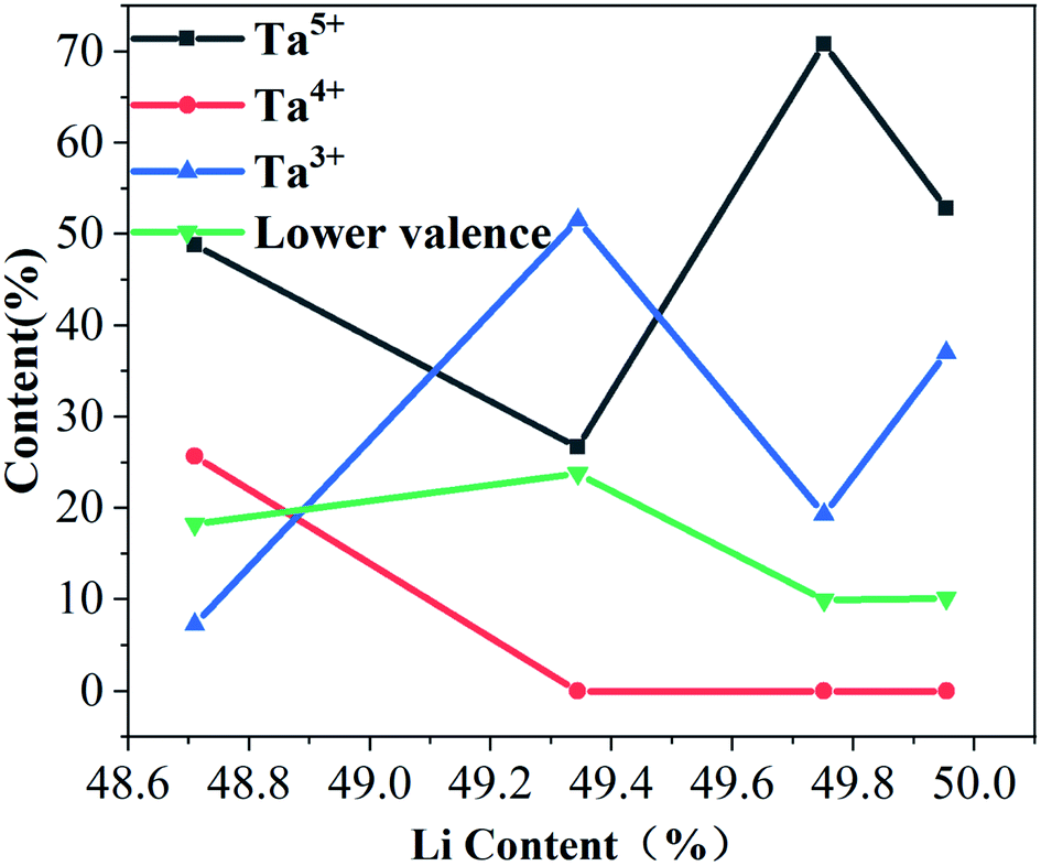 | ||
| Fig. 6 Proportion of Ta valence state with different Li content in LT crystal. | ||
From valence state analysis of the Ta4f electron layer of NSLT crystals, only the VLi and TaLi defect model could not explain the emergence of Ta3+ and other Ta valence states. Therefore, our analysis follows the following three principles: (1) ensure charge balance; (2) when the number of defects in LT crystal increases, the crystal density increases; and (3) there is an Li deficiency in CLT crystals.19 The lack of Li ions in the crystal will lead to the imbalance of positive and negative charges, which leads to the occurrence of defects in the VLi and Tali range. Some electrons in the crystal are attracted by TaLi4+ defects or TaTa5+ to form polarons, and the polarized Ta will shift, that is, lattice relaxation will occur. The mechanism of polariton formation is described in Schirmer's paper.32,33 The free polarons, bipolar polarons and bound polarons, proposed by Maaider et al., and NbLi defects are equivalent to NbV + VLi (NbLi defect shifts to the nearby octahedral oxygen site).20 Krampf et al. calculated that, according to the first principle, LT crystals also contain polarons, bipolar and bound polarons.34 We propose a new defect model of TaLi + VLi + polarons:
| free polaron: TaLi4+ + e → TaLi3+, TaTa + e− → TaTa− |
| bipolar polaron: TaTa5+ + 2e− → TaTa3+ |
Among these, TaLi3+ and TaTa− form bound polarons (TaTa−TaLi3+)2+.23,35 CLT crystals contain VLi, TaLi4+, VLi + TaV, bound polarons (TaTa−TaLi3+)2+ and TaLi3+, showing that CLT crystals can simultaneously contain Ta5+, Ta4+, Ta3+ and lower-valence Ta. When the Li concentration increases to 49.344%, VLi and a small proportion of TaLi4+ defects disappear due to the entry of Li, resulting in the disappearance of most Ta4+ in the XPS spectrum of the Ta4f electron layer. However, due to the entry of a large number of Li ions, the number of cations also increases. According to the principle of charge balance, the total price state of Ta ions decreases. Fig. 7 shows the XPS energy spectrum of the O1s electron layer. From this spectrum, the peak corresponding to its binding energy is divided into two peaks, and the peak binding energy is increased to varying degrees. This occurs because the binding energy corresponding to the XPS energy peak increases after the loss of electrons during the oxidation reaction, and the binding energy of electrons obtained in the reduction reaction decreases, indicating that O2− ions have lost some electrons. Since TaLi4+ defects absorb electrons more easily, these defects absorb an electron and become TaLi3+. When the Li ion concentration reaches 49.751%, the binding energy of O decreases; that is, several electrons are gathered by O atoms. At this point, a proportion of TaLi3+ becomes TaLi4+ defects again, and a small portion of bound polarons disappear and become TaLi4+ defects and TaTa5+ once more. As the Li content further increases, the TaLi4+ defects are replaced by Li again, resulting in a large number of Ta5+ ions. When the Li content continues to increase, the O binding energy decreases, indicating that the octahedral O obtains some electrons. However, the decrease is small, indicating that the electrons available from octahedral O are close to saturation. At this point, the Ta5+ content decreases and Ta3+ content increases, while that of lower-valence Ta does not significantly change. This implies that TaTa is more likely to absorb one electron to form a bound polaron with an adjacent TaLi3+, or absorb two electrons to become Ta3+.
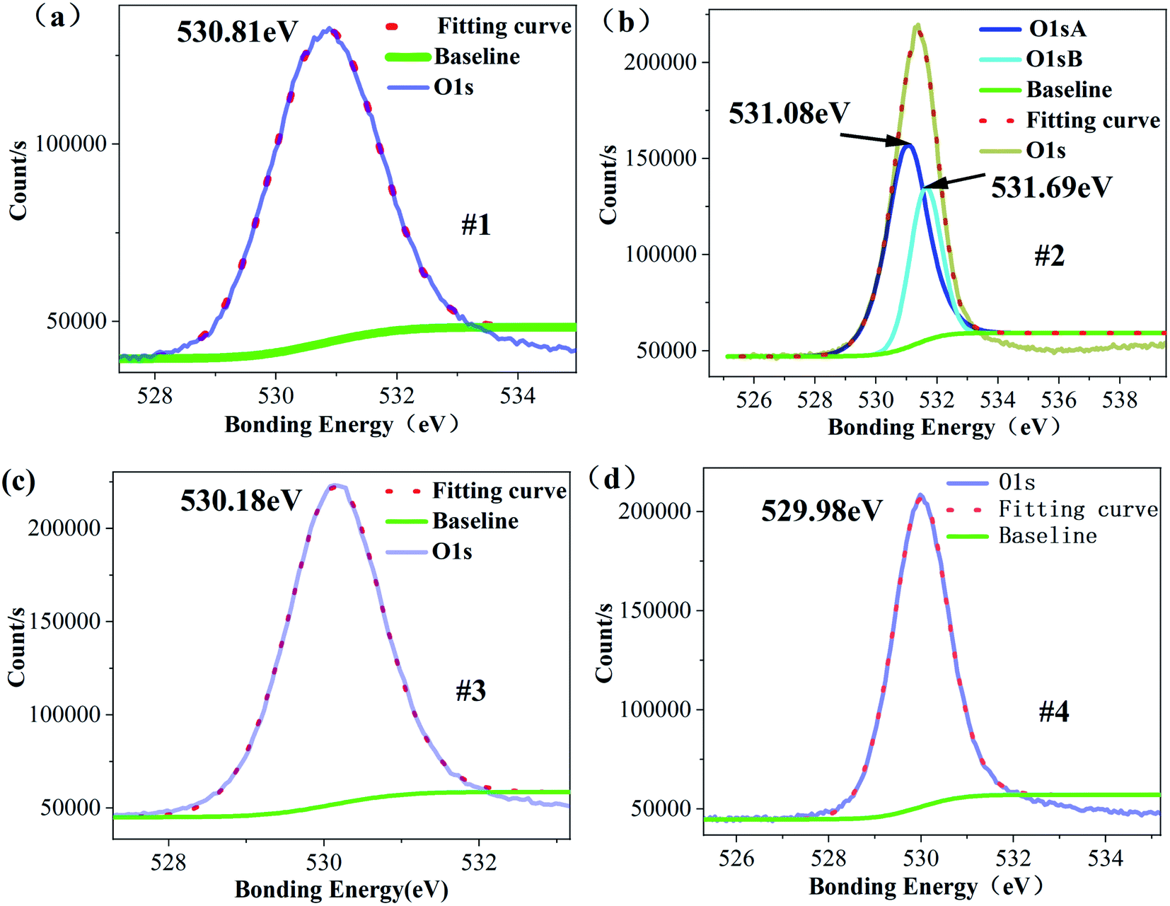 | ||
| Fig. 7 XPS energy spectrum peak splitting fitting of electrons in O1s layer (a) #1 (b) #2 (c) #3 (d) #4. | ||
To summarise, with increasing Li content in LT wafers, Li vacancy defects and TaLi4+ defects essentially disappear. However, when Li:Ta = 1:1, a large amount of TaTa3+ species appears. When the Curie temperature is 677.23 °C and the Li content is 49.751%, the LT wafer contains the highest amount of Ta5+ ions and there is no Ta4+ in the wafer. The lattice structure of NSLT wafer tends to be perfect at this time; therefore, it is inferred that the performance of NSLT is also optimised at this time.
3.3 Raman spectroscopic analysis
Raman spectrum can characterize defects in the crystal. As can be seen from Fig. 8, #2, #3 and #4 have 13 Raman peaks, but #1 has only 11 Raman peaks # 1 sample has a Raman peak at 181 cm−1, but with the diffusion of Li ions, this peak is blue shifted. The peaks of #2, #3 and #4 samples are blue shifted to 163 cm−1, 166 cm−1 and 162 cm−1 respectively. And there is a companion peak at 460 cm−1, which has never appeared in the Raman spectra of NSLT crystals in other papers.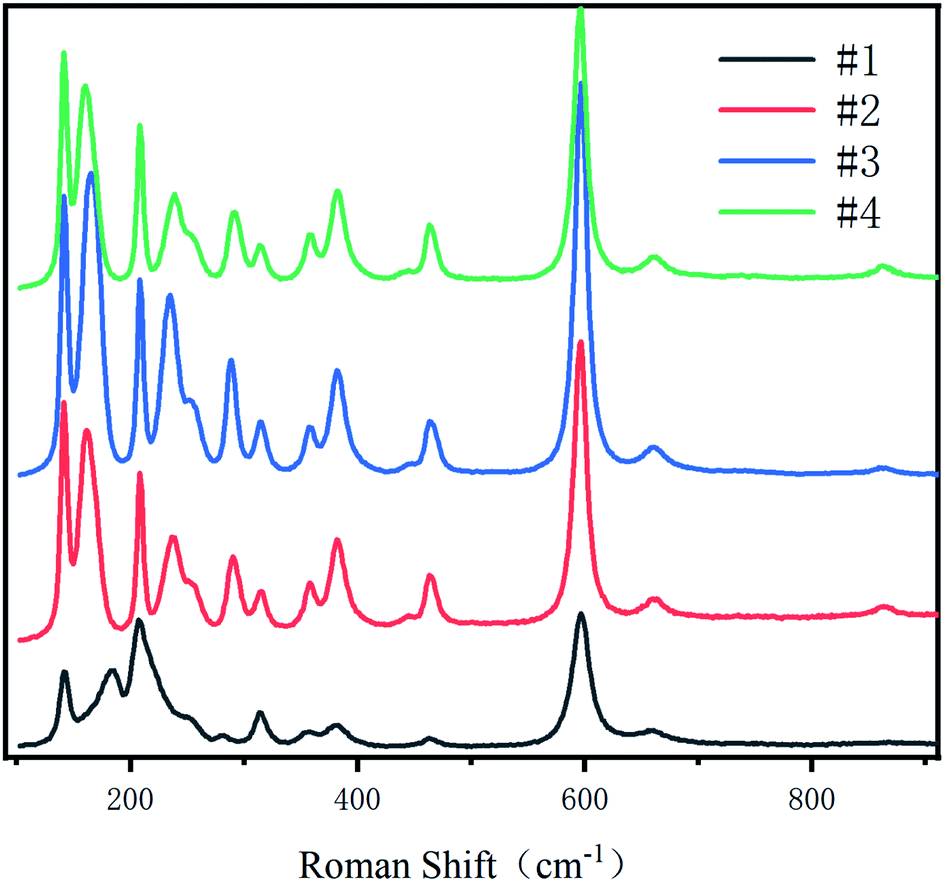 | ||
| Fig. 8 Raman spectrum. | ||
Because the Raman spectra of LT crystals with different Li contents have different baseline and the Raman peaks are not smooth, origin is used to process the Raman spectra. First, the baseline is subtracted from the original Raman spectrum; Secondly, the Raman peaks subtracted from the baseline were smoothed by savitzky Golay method; Finally, the Raman spectra were fitted with (Gaussian Lorentzian cross product) gussion lorentcross,36,37 and the Raman peaks near 160 cm−1, 460 cm−1 and 867 cm−1 of LT crystal were observed in Fig. 9.
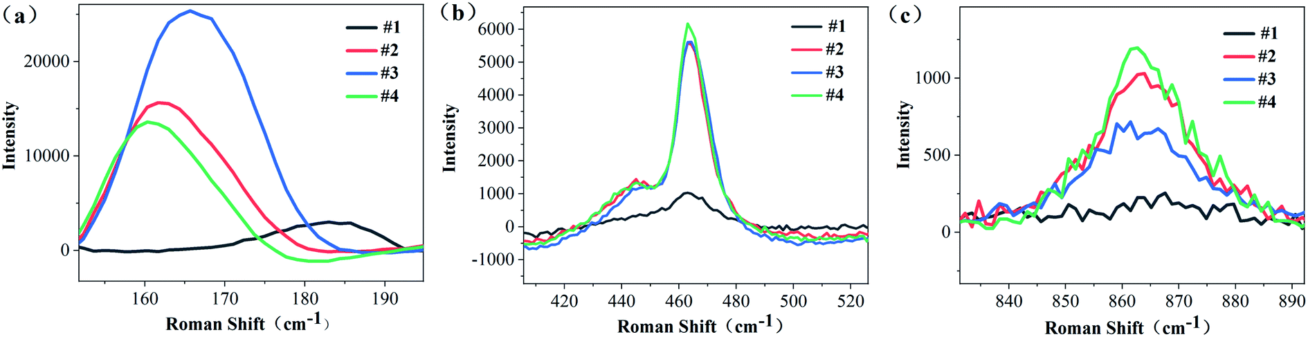 | ||
| Fig. 9 Raman spectral magnification (a) 160 cm−1 (b) 460 cm−1 (c) 867 cm−1. | ||
The substitution of Ta for Li reduces the translational property of the lattice, resulting in a large range of the wave vector k of the scattered rope in the Brillouin region, and the wide distribution of K leads to the increase of the Raman linewidth.38 From Fig. 10(a), it can be obtained that the CLT crystal has a Raman peak at 181 cm−1. However, as Li increases, this Raman peak is frequency shifted and the Raman half-peak width becomes smaller. It is obvious from Fig. 10(b) that there is a companion peak at 460 cm−1 in the Raman band, and this peak is associated with O ions, which proves that O ions change during the increase of Li content, leading to the companion peak in the Raman peak.39 When the wafer is a CLT crystal, the Raman shift is 460 cm−1 without this companion peak. With the increase of Li content, this companion peak appears and increases with the increase of Li content. Since Li and O form a weak Li–O bond, we consider this companion peak as the characteristic Raman peak of Li–O in this paper.40 This companion peak also demonstrates that the defect structure of the crystal changes with the diffusion of Li into it. Figure 10(c) shows the Raman peak near 863 cm−1. This peak characterizes the intrinsic defects within the LT crystal, with Raman half-peak widths of 65.95, 22.5, 22.47, and 24.62 for #1, #2, #3, and #4, respectively.41 The half-peak width of this peak did not tend to decrease all the time with increasing Li content, so this peak was subjected to Raman imaging to further investigate this peak.
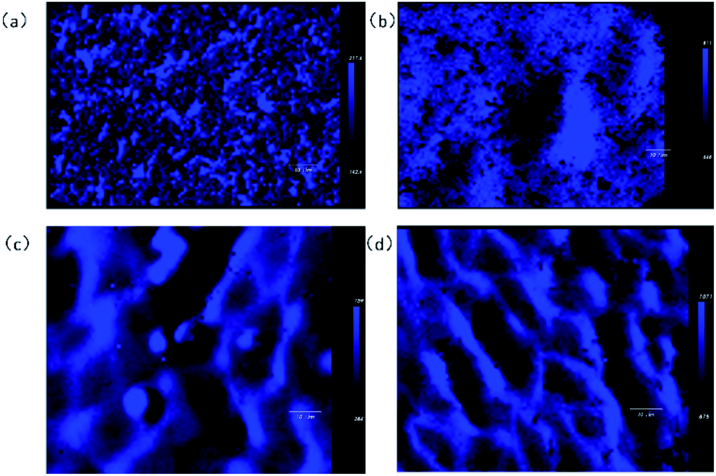 | ||
| Fig. 10 Raman peak intensity imaging. | ||
3.4 Raman imaging
In order to observe the atomic and stress distribution of NSLT crystals, the 863 cm−1 peak was observed by Raman imaging to observe the intrinsic defects and structure.From Fig. 10, it can be seen that the peak intensity of CLT is 217.4, while that of NSLT is 1071, with the diffusion of Li ions entering. From the analysis of peak intensity distribution, with the increase of Li content, the peak intensity distribution gradually converges and eventually presents a grid distribution, that is, the stress distribution is better concentrated, which also proves that the increase of Li content leads to the decrease of defects. The Peak Position Map also re-demonstrates that Li diffusion can lead to changes in local structure. From Fig. 11, we can see that with the increase of Li content, the red pixel points in the graph increase significantly, and the clustering of different pixel points occurs, especially in Fig. 11c.
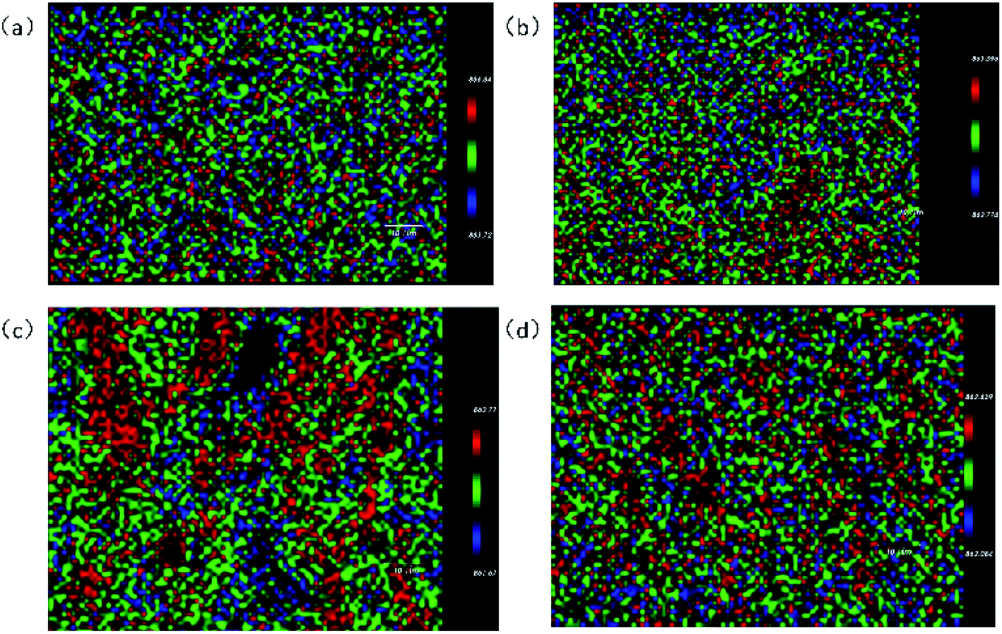 | ||
| Fig. 11 Raman peak location imaging. | ||
The peak intensity of Raman imaging demonstrates that the diffusion of Li leads to defect reduction and better ordering of atoms, but there are also some stress concentrations. From the peak position map of Raman imaging, it can be seen that the distribution of atoms in LT crystals is not very uniform, and the local disorder in LT crystals becomes more obvious with the diffusion of Li ions.
4 Conclusions
NSLT crystals with different Li contents was prepared by VTE method. The effects of different Li content on the internal structure of LT wafers and on the mechanism of defect formation were discussed. The Curie temperature of LT wafers treated by VTE increased significantly, and the Curie temperature is positively correlated with the Li content in the LT crystals. Therefore, the Li content increased in LT crystals treated by VTE.From the XPS spectrum of NSLT crystals, it was concluded that the crystal contains Ta in various valence states. The entry of Li ions leads to a large increase of cations in the crystal, which changes the gain and loss of electrons and the peak binding energies of Ta and O. LT crystals contain Ta5+, Ta4+, Ta3+ and lower-valence Ta. Ta4+ appears due to the occurrence of a Ta inversion defect, and a portion of Ta4+ ions absorb one electron to form Ta3+. The absorption of electrons leads to the shift of the Ta3+ position and the formation of a bound polaron with TaTa4+ which absorbs one electron, resulting in the emergence of lower-valence Ta. When the Li content increases, the VLi vacancies and a small portion of TaLi4+ disappears, and another portion of TaLi4+ absorbs an electron to become TaLi3+. Due to the injection of a large number of cations, part of TaTa5+ absorbs an electron and becomes TaTa4+, forming a bound polaron (TaTa−TaLi3+)2+ with TaLi3+. At this time, the relative proportion of Ta5+ decreases, Ta4+ disappears completely, and the proportion of Ta3+ and lower-valence Ta increases. When the Li content increases to 49.751%, O absorbs some electrons. A portion each of TaLi3+, TaTa4+ and TaLi3+ in the form of bound polarons (TaTa−TaLi3+)2+ disappear, and Li returns to the original octahedral O site. TaLi4+ changes back to Ta5+, but a small part of TaLi3+ and (TaTa−TaLi3+)2+ remain. When the Li content increases to 49.947%, part of TaTa5+ absorbs two electrons and becomes TaTa3+. This leads to a decrease in Ta5+ and an increase in Ta3+, while the proportion of lower-valence Ta remains unchanged. Local distortions on the wafer surface and local structural disorder affecting the valence state of Ta are also seen from Raman spectra and Raman imaging. From the above analysis, the mixed defect model of polarons, Li vacancies and Ta inversions is more suitable to describe the Ta valence changes.
The results show that when the content of Li is 49.751%, this is the inflection point with regards to the proportion of Ta5+. Compared with other tested samples, the lattice of this NSLT crystal is closest to the perfect lattice, and so it is speculated that the physical properties of the NSLT crystal are optimised at this Li content. In future work, we will continue to explore the best inflection point of Ta5+ content in NSLT crystals. Exploring the optimal performance of Li concentration in NSLT crystals is a prospective work for its future applications, such as optical resonators based on NSLT crystals, surface acoustic wave filters, and so on. There are still some questions to be answered in this work, including whether Ta3+ exists as TaTa3+ or TaLi3+ when the Li content is 49.751%, and whether or not TaTa5+ is more inclined to absorb two electrons to form TaTa3+. Answering these questions will also require us to further study and clarify the defect mechanism of NSLT crystals.
Author contributions
All authors contributed to the study conception and design. Material preparation, data collection and analysis were performed by Xuefeng Xiao, Qingyan Xu and Shuaijie Liang. The first draft of the manuscript was written by Xuefeng Xiao and Qingyan Xu and all authors commented on previous versions of the manuscript. All authors read and approved the final manuscript.Conflicts of interest
There are no conflicts to declare.Acknowledgements
This research was funded by the Fundamental Research Funds for the Central Universities, North Minzu University (2020DXXY002 and 2021KJCX07), the National Natural Science Foundation of China (61965001 and 11864001), the Ningxia Province Key Research and Development Program (2018BEE03015 and 2021BEE03005), the Natural Science Foundation of Ningxia (2019AAC03103 and 2020AAC03239), the Ningxia first-class discipline and scientific research projects (electronic science and technology) (NXYLXK2017A07). The authors thank the Ningxia new solid electronic materials and Devices research and development innovation team, the Ningxia advanced intelligent perception control innovation team and the Ningxia acoustooptic-crystals industrialization Innovation team.References
- M. Kadota, Y. Ishii and S. Tanaka, IEEE Trans. Ultrason. Ferroelectr. Freq. Control, 2020, 68(5), 1955–1964 Search PubMed.
- S. G. Porter, Ferroelectrics, 1981, 33(1), 193–206 CrossRef CAS.
- S. C. Peng, X. Y. Chen and G. C. Liu, Technical Acoustics, 2009, 28(4), 137–139 Search PubMed.
- N. E. Yu, S. Kurimura, Y. Nomura and K. Kitamura, Jpn. J. Appl. Phys., 2004, 43(10A), L1265 CrossRef.
- S. Kumaragurubaran, S. Takekawa, M. Nakamura and K. Kitamura, J. Cryst. Growth, 2006, 292(2), 332–336 CrossRef CAS.
- E. Y. Nan, S. Kurimura, Y. Nomura, M. Nakamura, K. Kitamura, J. Sakuma, Y. Otani and A. Shiratori, Appl. Phys. Lett., 2004, 84(10), 1662–1664 CrossRef.
- E. Y. Nan, S. Kurimura, M. Nakamura , Y. Namura, K. Kitamura, J. Sakuma, Y. Otani and A. Shiratori, Conference on Lasers and Electro-Optics, IEEE, 2003 Search PubMed.
- A. G. Getman, S. V. Popov and J. R. Taylor, Appl. Phys. Lett., 2004, 85(15), 3026–3028 CrossRef CAS.
- A. A. Esin, A. R. Akhmatkhanov and V. Y. Shur, Ferroelectrics, 2016, 496(1), 102–109 CrossRef CAS.
- N. Masaif, I. Lagrat and H. Hboub, Indian J. Phys. Proc. Indian Assoc. Cultiv. Sci, 2022, 96(2), 411–417 CAS.
- C. S. Abrahams and P. Marsh, Acta Crystallogr., Sect. B:, 1986, 42(1), 61–68 CrossRef.
- M. Palatnikov, O. Shcherbina, V. Sandler, N. Sidorov and K. Bormanis, Ferroelectrics, 2011, 417(1), 46–52 CrossRef CAS.
- J. Imbrock, D. Kip and E. Krtzig, Opt. Lett., 1999, 24(18), 1302–1304 CrossRef CAS PubMed.
- A. Huanosta and A. R. West, J. Appl. Phys., 1987, 61(12), 5386–5391 CrossRef CAS.
- K. Kitamura, S. Takekawa, M. Nakamura, S. Kurimura and O. Louchev, Quantum Electronics & Laser Science Conference, IEEE, 2005 Search PubMed.
- P. Lerner, C. Legras and J. P. Dumas, J. Cryst. Growth, 1968, 3, 231–235 CrossRef.
- S. Kim, V. Gopalan, K. Kitamura and Y. Furukawa, J. Appl. Phys., 2001, 90(6), 2949–2963 CrossRef CAS.
- K. F. Chen, Y. L. Li, C. Peng, Z. Lu, X. Y. Luo and D. F. Xue, Inorg. Chem. Front., 2021, 8(17), 4006–4013 RSC.
- C. Leroux, G. Nihoul, G. Malovichko, V. Grachev and C. Boulesteix, J. Phys. Chem. Solids, 1998, 59(3), 311–319 CrossRef CAS.
- K. Maaider, N. Masaif and A. Khalil, Indian J. Phys., 2020, 95(2), 1–6 Search PubMed.
- F. Abdi, M. D. Fontana, M. Aillerie and P. Bourson, Appl. Phys. A, 2006, 83(3), 427–434 CrossRef CAS.
- N. Iyi, K. Kitamura, F. Izumi, J. K. Yamamoto, T. Hayashi, H. Asano and S. Kimura, J. Solid State Chem., 1992, 101(2), 340–352 CrossRef CAS.
- J. M. Shi, H. Fritze, G. Borchardt and K. D. Becker, Phys. Chem. Chem. Phys., 2011, 13(15), 6925–6930 RSC.
- B. Faust, H. Müller and O. F. Schirmer, Ferroelectrics, 1994, 153(1), 297–302 CrossRef.
- F. Schmidt, A. L. Kozub, U. Gerstmann, D. T. Schmidt and A. Schindlmayr, Crystals, 2021, 11(542), 1–18 Search PubMed.
- X. F. Xiao, H. Zhang and X. F. Zhang, J. Mater. Sci.: Mater. Electron., 2020, 31, 16414–16419 CrossRef CAS.
- J. F. Yang, Q. H. Mao, J. F. Shang, H. S. Hao, Q. L. Li, C. X. Huang, L. Zhang and J. Sun, Mater. Lett., 2018, 232, 150–152 CrossRef CAS.
- M. V. Ivanov, T. V. Perevalov, V. S. Aliev, V. A. Gritsenko and V. V. Kaichev, J. Exp. Theor. Phys., 2011, 112(6), 1035–1041 CrossRef CAS.
- D. H. Sun, Growth and Properties of Lithium Tantalate/Lithium Niobate Crystals of Periodically Polarized Matrix Materials[D], Shan Dong University, 2015 Search PubMed.
- O. Y. Khyzhun, E. A. Zhurakovsky, A. K. Sinelnichenko and V. A. Kolyagin, J. Electron Spectrosc., 1996, 82(3), 179–192 CrossRef CAS.
- F. Gitmans, Z. Sitar and P. Günter, Vacuum, 1995, 46(8–10), 939–942 CrossRef CAS.
- O. F. Schirmer, M. Imlau, C. Merschiann and B. Schoke, J. Phys.: Condens. Matter, 2009, 21(12), 123201 CrossRef CAS PubMed.
- H. H. Nahm and C. H. Park, Phys. Rev. B, 2008, 78(18), 184108 CrossRef.
- A. Krampf, M. Imlau, Y. Suhak, H. Fritze and S. Sanna, New J. Phys., 2021, 23(3), 033016 CrossRef CAS.
- C. Merschjann, B. Schoke, D. Conradi, M. Imlau and K. Polgar, J. Phys.: Condens. Matter, 2008, 21(1), 015906 CrossRef PubMed.
- V. S. Gorelik, S. D. Abdurakhmonov, N. V. Sidorov and M. N. Palatnikov, Inorg. Mater., 2019, 55(5), 524–532 CrossRef CAS.
- S. Sanna, S. Neufeld, M. Rüsing, G. Berth, A. Zrenner and W. G. Schmidt, Phys. Rev. B, 2015, 91(22), 224302 CrossRef.
- U. Schlarb, S. Klauer, M. Wesselmann, K. Betzler and M. Wöhlecke, Appl. Phys. A, 1993, 56(4), 311–315 CrossRef.
- Y. Repelin, E. Husson, F. Bennnani and C. Proust, J. Phys. Chem. Solids, 1999, 60(6), 819–825 CrossRef CAS.
- M. Petrowsky and R. Frech, J. Phys. Chem. B, 2010, 114(26), 8600–8605 CrossRef CAS PubMed.
- Z. F. Guo, Inorg. Chem. Industry, 2021, 53(10), 70–73 Search PubMed.
Footnote |
| † Both authors contributed equally to this work. |
| This journal is © The Royal Society of Chemistry 2022 |