
 Open Access Article
 This Open Access Article is licensed under a Creative Commons Attribution-Non Commercial 3.0 Unported Licence
Highly-stable flexible pressure sensor using piezoelectric polymer film on metal oxide TFT†
Taiyu Jin a,
Sang-Hee Ko Parkb and
Da-Wei Fang*a
a,
Sang-Hee Ko Parkb and
Da-Wei Fang*a
aInstitute of Rare and Scattered Elements, College of Chemistry, Liaoning University, Shenyang 110036, P. R. China. E-mail: davidfine@163.com
bSmart & Soft Materials & Devices Laboratory (SSMD), Department of Materials Science and Engineering, Korea Advanced Institute of Science and Technology (KAIST), Daejeon 34141, South Korea
First published on 21st July 2022
Abstract
In this study, a flexible pressure sensor with highly stable performance is presented. The pressure sensor was fabricated to work under low voltage conditions by using a high mobility amorphous indium–gallium–zinc oxide (a-IGZO) thin-film transistor (TFT) and a stretched polyvinylidene fluoride (PVDF) film. To prepare a stable sensor suitable for practical use, we designed a device structure that shields ambient noise by grounding the control gate. The shielding structure significantly improves the stability of the device. Moreover, the sensor was fabricated on a flexible substrate and delaminated via a laser lift-off (LLO) technique to meet the urgent needs for flexibility. The pressure sensor showed good sensitivity and reliability over a pressure ranging from 0 to 75 kPa which covers the human touch pressure range. Especially, good linearity over a wide pressure range and high stability over 1000 repeated loadings were realized. Due to the simple structure, the pressure sensor demonstrates the advantage of being inexpensive to be manufactured and holds the potential to be integrated into the display backplane. Therefore, the proposed sensor has great potential in the production of flexible touch screens, human–machine interacting applications, and even electronic skins in the future.
Introduction
With the increasing popularity of smartphones and wearable devices, consumers are placing higher demands on human–computer interaction. To recognize touch more accurately, advanced touch sensors have attracted a great deal of interest.1,2 Conventional touch screens do not recognize pressure levels, so they cannot meet the need for accurate recognition of touch. In contrast, emerging sensors are providing pressure level as an additional sensing parameter. With the physical support required for accurate touch sensing, smart devices are able to achieve diverse human–machine interaction eventually. In addition, driven by the growing market share of flexible displays and wearable devices, research on touch panels should also focus on durability and flexibility, as well as barrier-free integration with the portable devices.In recent years, studies have been reported on different methods of fabricating pressure sensors or tactile sensors. Typical pressure sensors are usually categorized by their transducing mechanisms. Piezoresistive sensors are devices that recognize pressures by converting mechanical changes into resistive signals. Most piezoresistive pressure sensors are achieved by building a three-dimensional microporous conductive network or a variable interface between the electrode and the active material.3–5 Due to the simple device structure and the simple working mechanism, these sensors have been studied quite intensively.6,7 A piezoresistive rubber was also fabricated into an organic TFT to realize a large-area sensitive flexible e-skin.8 Capacitive sensors are devices that converting mechanical changes into capacitive signals by changing separation distances or overlapped areas of two electrodes. A capacitive pressure sensor using elastomer dielectric layer with micro airgap was developed.9 In order to design high performance pressure sensors, various materials are used in pressure sensitive layers.10–14 However, both piezoresistive and capacitive pressure sensors have integration issues when manufactured with other components such as displays.15–17
Piezoelectric sensors are another type of pressure sensor that primarily measure the voltage across a piezoelectric layer generated by external pressure. Due to the fascinating piezoelectric property, some piezoelectric sensors can be even made into self-powered.18 Usually, ceramic materials such as Lead Zirconate Titanate (PZT) are chosen as high-performance piezoelectric materials because of their high piezoelectric coefficients. Nanogenerators and acoustic sensors using such inorganic materials have been deeply investigated.19,20 However, inorganic piezoelectric materials are usually too brittle to be used in flexible devices. Also, due to the toxicity of the lead component, the application of PZT is very limited. Therefore, a large number of studies have been shifted to organic piezoelectric materials, because of the superior biocompatibility, high mechanical flexibility, and low cost.21 Generally, PVDF and its copolymers are among the most widely used organic piezoelectric materials due to the high piezoelectric constants.22,23 Bae et al. reported a graphene-P(VDF-TrFE) multilayer film to work as an acoustic actuator and nano generator.24 However, studies on the preparation of touch sensors using PVDF are very limited. Because PVDF films are prone to external interference, and they should also be compatible with the underlying screen panel process when making touch sensors.
Transistors are often used to enhance the performance of piezoelectric pressure sensors. Both organic transistor and silicon transistor have been reported in the fabrication of piezoelectric pressure sensors.25,26 Metal-oxide semiconductors are widely used in driving thin-film transistors (TFTs) in display panels, because TFTs based on metal-oxide semiconductors show the advantages of lower off-state current, higher electron mobility, and high transparency in the visible band compared to traditional amorphous silicon materials.27 Amorphous indium–gallium–zinc–oxide (a-IGZO) is one of the most widely used metal-oxide semiconducting materials. Nevertheless, the internal defects in a-IGZO always make the device stability a major issue. Lots of work have been reported to improve the stability of metal-oxide semiconductor transistors.28 Pressure sensors using a-IGZO transistors have also been reported. Geng et al. fabricated a pressure sensor containing piezoelectric capacitor using a dual-gate a-IGZO TFT.29 But the complex process of the device is not suitable for integration into the screen, and the performance is not very ideal. When applying a-IGZO transistors to pressure sensors, stability is still a serious problem due to the harsh working environment. In addition, piezoelectric films are also susceptible to external influences. So, the studies on the combination of these two materials to prepare stable pressure sensors are limited. It is more important to improve the working stability of the sensor than to improve the performance of the sensor. Therefore, in order to make the sensor suitable for practical touch applications, the transistor enhanced piezoelectric sensor needs to build a structure in a low-cost way and improve the working stability of piezoelectric pressure sensors based on metal oxide semiconductor TFTs.
In this study, a piezoelectric pressure sensor was fabricated by stacking a PVDF film directly on a high-mobility a-IGZO TFT. In order to stabilize the output signal of the device, we have grounded the control gate to eliminate the influence of the surrounding environment. Compared with unshielded devices, the proposed pressure sensor exhibits a reliable response to external interference. Moreover, the sensor was made flexible via a laser lift-off (LLO) technique. The output of the sensor shows a strong correlation with the loading pressure ranging from 0 to 75 kPa, indicates a satisfactory linearity over a wide pressure range. The advantages of the piezoelectric material in dynamic sensing and working reliability were clearly verified through electrical characterization along with 1000 cycles of repeated pressure loadings. Showing great application potential for future display devices, we hope that the proposed pressure sensor can be used for various flexible human–interacting applications.
Experimental
Fabrication
Fig. 1a shows the schematic of the flexible pressure sensor. Generally, the sensor could be mainly divided into two parts: pressure-sensing piezoelectric capacitor and signal amplifying transistor. The two parts were developed and characterized separately.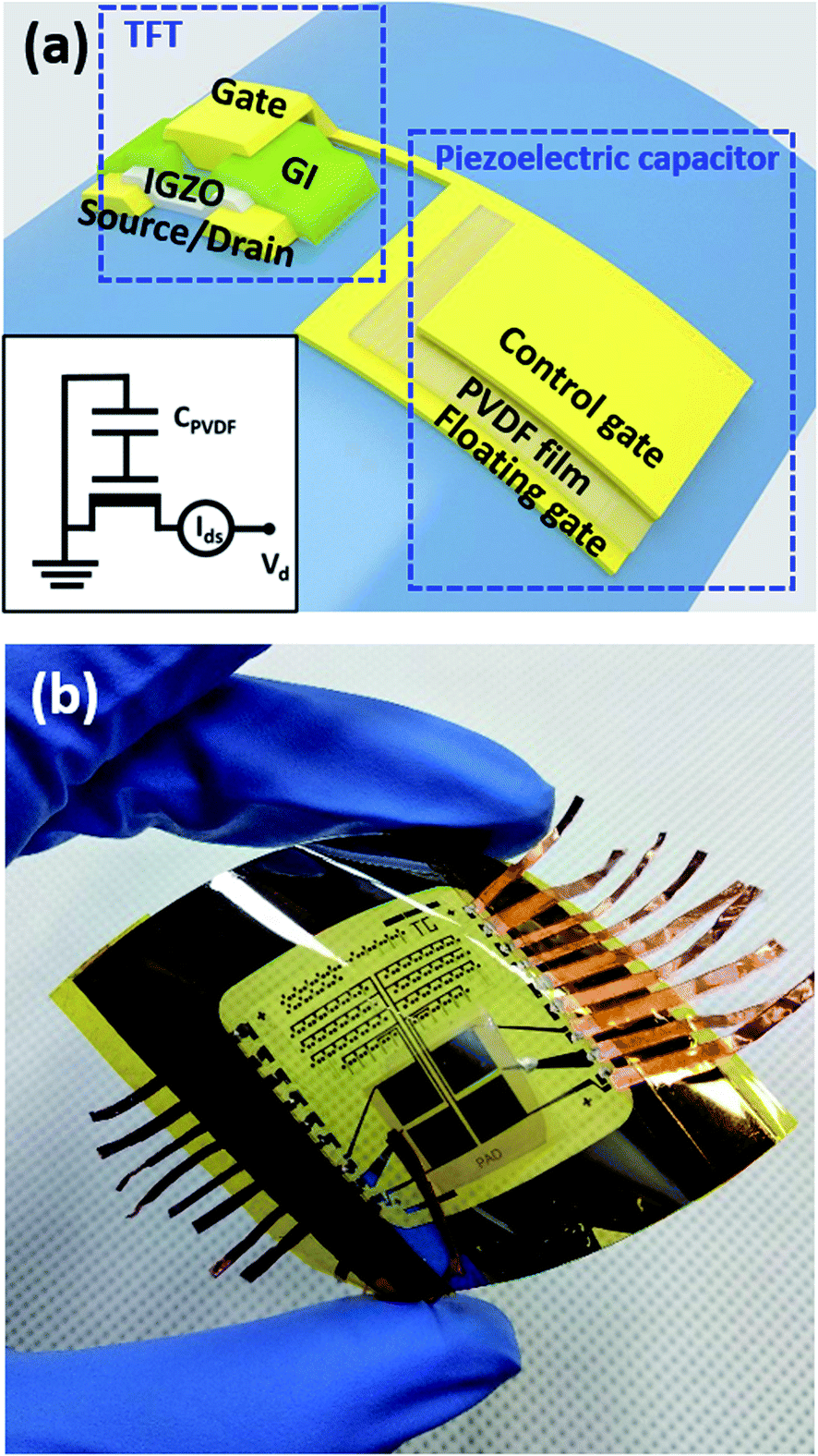 | ||
| Fig. 1 (a) Schematic of the sensor structure. Inset shows the circuit diagram of the sensor measurement. (b) Photo image of the pressure sensor fabricated on flexible substrate. | ||
To fabricate a flexible metal oxide TFT, a polyimide (PI) coated glass substrate was prepared. PI solution was spin-coated on a glass substrate and dried on a hot plate at 200 °C for 10 min. SiNx/AlOx buffer layer was then deposited as a water and hydrogen diffusion barrier. The metal oxide TFT is top-gate bottom-contact structure, as is the conventional transistor structure for the piezoelectric pressure sensor.30 During TFT fabrication, an indium-doped tin oxide (ITO) film with thickness of 150 nm was evaporated by a magnetron sputtering system and further patterned as source/drain electrodes. In order to get high current level, the channel width and length of the TFT are defined as 2560 μm and 20 μm, respectively (Fig. S1†). Then, we deposited IGZO for 40 nm as an active channel layer. The 40 nm-thick Al2O3 gate insulator layer was formed by plasma enhanced atomic layer deposition (PEALD) method at temperature of 200 °C. Finally, molybdenum metal film with thickness of 150 nm was sputtered as the top gate layer of the TFT. Specified patterns were formed by photolithography and chemical etching process after each layer deposition. The electrical properties of the TFTs were then characterized by a semiconductor analyzer. In order to form a flexible device, PI film was then delaminated from the glass by a LLO procedure.
Characterization and measurement
The pressure-sensing capacitor consists of a layer of piezoelectric film and a set of two electrodes on upper and lower sides of the film. Commercially available stretched 28 nm-thick PVDF film was used as a piezoelectric layer. To confirm the crystallinity and the chain orientation of the PVDF film, XRD and FT-IR measurements of the film were conducted. A layer of Mo film was subsequently sputtered on top of the PVDF film to work as an upper electrode of the sensing capacitor, then the sputtered film was attached to the extended top gate electrode of the TFT. So that the extended gate electrode could work as a lower electrode of the piezoelectric film, forming a sandwiched structure. Upper and lower square-shaped electrodes were positioned face to face, and aligned carefully to ensure the largest overlap area. Unit area of the sensing capacitor is 0.25 cm2. Fig. 1b shows the photo image of the fabricated flexible pressure sensor.After the sensor fabrication, we have evaluated the sensing properties by a hand-made pressure test system. The system was built by assembling an automated mechanical test stand (Mark-10, ESM 303) and a force gauge (Mark-10, M5-2) together (Fig. S2†). The pressure values were recorded by a computer. On the other hand, a semiconductor analyser was connected to the sensor, continuously monitoring the drain current of the TFT which can be considered as the output signal. All electrical measurements were conducted at room temperature with ambient air pressure condition.
To test the sensor, 0.1 V was applied to the sensor's TFT Vsd and the current between the source-drain was recorded in real time using a semiconductor analyser. When continuously applying a pressure of 8 kPa to the sensor at a speed of 50 mm min−1, the output currents in the shielded, unshielded, and disturbed states of the device were compared. The shielded state refers to the control gate being grounded to shield interference. The unshielded state refers to the control gate does not come into contact with any electrodes. The disturbed state refers to applying a −1 V to 1 V interference voltage, or adding a piece of debris to the test environment, when the device is in the unshielded state. In order to measure the sensitivity of the sensor to different pressures, the current output of the sensor was continuously monitored when different pressures such as 2 kPa, 4 kPa, 8 kPa, 17 kPa, 35 kPa, and 75 kPa were applied to the sensor. Each pressure was repeated 10 times at a speed of 50 mm min−1, and the average current value for each pressure level was calculated. To verify the consistency of the sensor's pressure recognition, the sensor output in the pressure reduction sequence (75 kPa, 35 kPa, 17 kPa, 8 kPa, 4 kPa, and 2 kPa) was also measured. Finally, to ensure data stability during long-term operation, 1000 cycle loading–unloading test was performed in the sensor. Each cycle consists of four steps: loading 75 kPa, wait for 2 s, pressure unloading, and wait another 2 s. The speed of pressure loading and unloading was set to 50 mm min−1.
Results and discussion
Circuit
The inset of Fig. 1a shows the equivalent circuit diagram of the sensor measurement. Normally, the drain current of a TFT is controlled by the voltage applied on the TFT gate electrode. However, the full surface coverage of the PVDF film resulted in the isolated TFT gate electrode between the gate insulator layer and the polymeric film. Therefore, the voltage generated when the external pressure is loaded on the PVDF film is a key factor in changing the working state of the TFT. On the other hand, since the potential of the control gate remains constant, the potential of the lower surface (Floating Gate) is completely reflecting the voltage across the piezoelectric film. As a result, the pressure causes the TFT gate voltage to change, thereby affecting the current between the source and drain electrodes. By monitoring the drain current, the pressures applied to the sensor can be obtained.A large number of studies have reported on the pressure sensors based on the combination of piezoelectric films and field-effect transistors, most of which were based on covering the film directly on a transistor.31 However, the direct covering of the piezoelectric film shows several disadvantages. Firstly, the active part of the transistor is usually quite small, so the area where pressure sensing can be performed is limited. In addition, due to the vertical stacking structure of the pressure sensing capacitor and the semiconductor layer, the semiconductor layer is prone to failure owing to the vertical stress during the pressure-sensing process. Some research groups have even reported that the tiny inner-pressure of the film generated during deposition could influence the electrical properties of the transistor.32 Therefore, we have spatially separated the two parts and increased the sensing area to improve the sensing ability. In the future, the surface of the semiconductor region will be coated with a hard insulating material to reduce external mechanical and electrical influences.
Piezoelectric film
PVDF is a polymer compound composed of repeated CH2–CF2 subunits, which often exhibits a semi-crystalline structure. Generally speaking, there are α, β, γ, and δ four different possible crystal phases appear in PVDF.33 Among these structures, β phase, due to its ferroelectric crystalline structure, plays a key role in piezoelectric properties. Therefore, the PVDF film containing only β-phase inside is the most ideal material in this study. In this work, a mechanically stretched PVDF film was used along with a layer of conductive coating on the surface as a pressure sensing element. In order to apply piezoelectric films to pressure sensitive capacitors, the presence of the piezoelectric β-phase was confirmed by XRD and FTIR spectroscopy.A room-temperature X-ray diffraction (XRD) method was used to characterize the crystallinity degree of the PVDF film. Fig. 2a shows the XRD data scanned in the 2θ mode ranging from 15 to 30° with a step interval of 0.01°. The curve exhibits sharp diffraction peaks at 2θ = 20.6° which is reflecting the angular position of the (200) or (110) crystal plane in PVDF polymer. According to the literature survey, this characteristic peak can be categorized to the orthorhombic β-phase.34,35 If the PVDF film contains other phases, a peak that can be classified as the (100) or (020) crystal plane will be displayed at around 18.5°, corresponding to the α phase or the γ phase.36,37
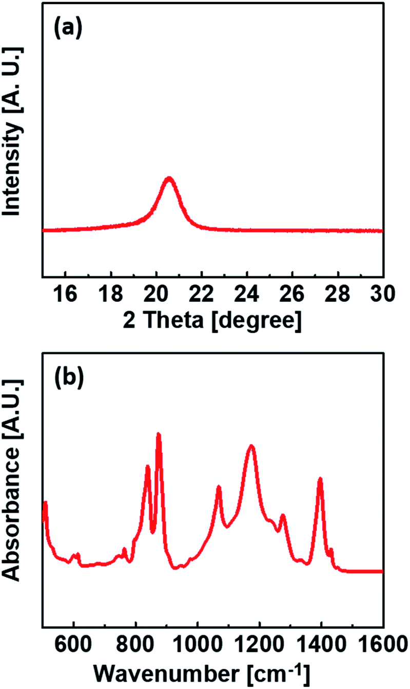 | ||
| Fig. 2 (a) XRD and (b) FTIR absorbance data of the stretched PVDF film. | ||
FTIR spectrum is effective for revealing the molecular orientation of the polymer. As the orientation of the groups in the polymer chain changes during film stretching, the assignment of each characteristic absorption band in the FTIR spectra is essential for explaining the rotation of the polymer chain. As shown in Fig. 2b the presence of intensive peaks at 839 cm−1 (CF2 symmetric stretching and C–C bond stretching) and 1290 cm−1 (trans band) indicating that the polymer has a strong β-phase crystal.33,38 This result is consistent with the XRD result, indicating that the stretched PVDF film can be used to fabricate pressure sensors without further processing.
To confirm the piezoelectric properties of the PVDF film, we used an oscilloscope to measure the voltage generated across the piezoelectric film. Fig. S3† shows that voltages can be generated across the piezoelectric film in the presence of external pressure, and the peak of the voltage increases as the load force increases. Voltage peaks generated under normal pressures are always in the same direction. However, after exchanging the connections between the upper and lower electrode contacts, the direction of the peak is reversed.37,39 In order to verify the properties of the unstretched films, we tried to prepare PVDF films without poling and stretching. Commercially available PVDF powder (Solvay) was dissolved in a co-solvent (methyl ethyl ketone and acetone mixed at ratio of 1![[thin space (1/6-em)]](https://www.rsc.org/images/entities/char_2009.gif) :1 in volume). After 24 hour sonication, the solution was then deposited on a slide glass for 30 μm thick by a doctor blade and annealed at 130 °C for 1 hour to evaporate the solvent. The film was then peeled off from the glass substrate and conducted the same pressure measurement. As a result, the film did not show the same piezoelectric properties. This result proves that the stretched PVDF film does have an excellent piezoelectric property and therefore can be used in the device we have proposed above.
:1 in volume). After 24 hour sonication, the solution was then deposited on a slide glass for 30 μm thick by a doctor blade and annealed at 130 °C for 1 hour to evaporate the solvent. The film was then peeled off from the glass substrate and conducted the same pressure measurement. As a result, the film did not show the same piezoelectric properties. This result proves that the stretched PVDF film does have an excellent piezoelectric property and therefore can be used in the device we have proposed above.
Metal oxide TFT
Metal oxide TFTs with high mobility were fabricated into the sensor to amplify the voltage obtained through the piezoelectric film. The TFTs were fabricated on a PI-coated glass substrate to prepare a flexible device, and the PI supported TFTs were delaminated from the glass by a LLO technique. Fig. 3a shows the transfer characteristics of the a-IGZO TFT. The transfer curve before lift-off was measured on a rigid substrate, while the measurement after lift-off was conducted on a flexible PI substrate. The voltage between source and drain electrodes were fixed at 0.1 V, and sweeping gate voltage was from −5 V to 5 V with a step of 0.14 V. Before LLO, the n-type IGZO TFT exhibits a relatively high mobility of 12.17 cm2 V−1 s−1 as we previously reported.40 The subthreshold swing, hysteresis, and threshold voltage values were 0.11 V dec−1, 0.22 V, and −0.66 V, respectively. Based on the above results, we conclude that the TFTs are suitable for driving sensors at low voltage.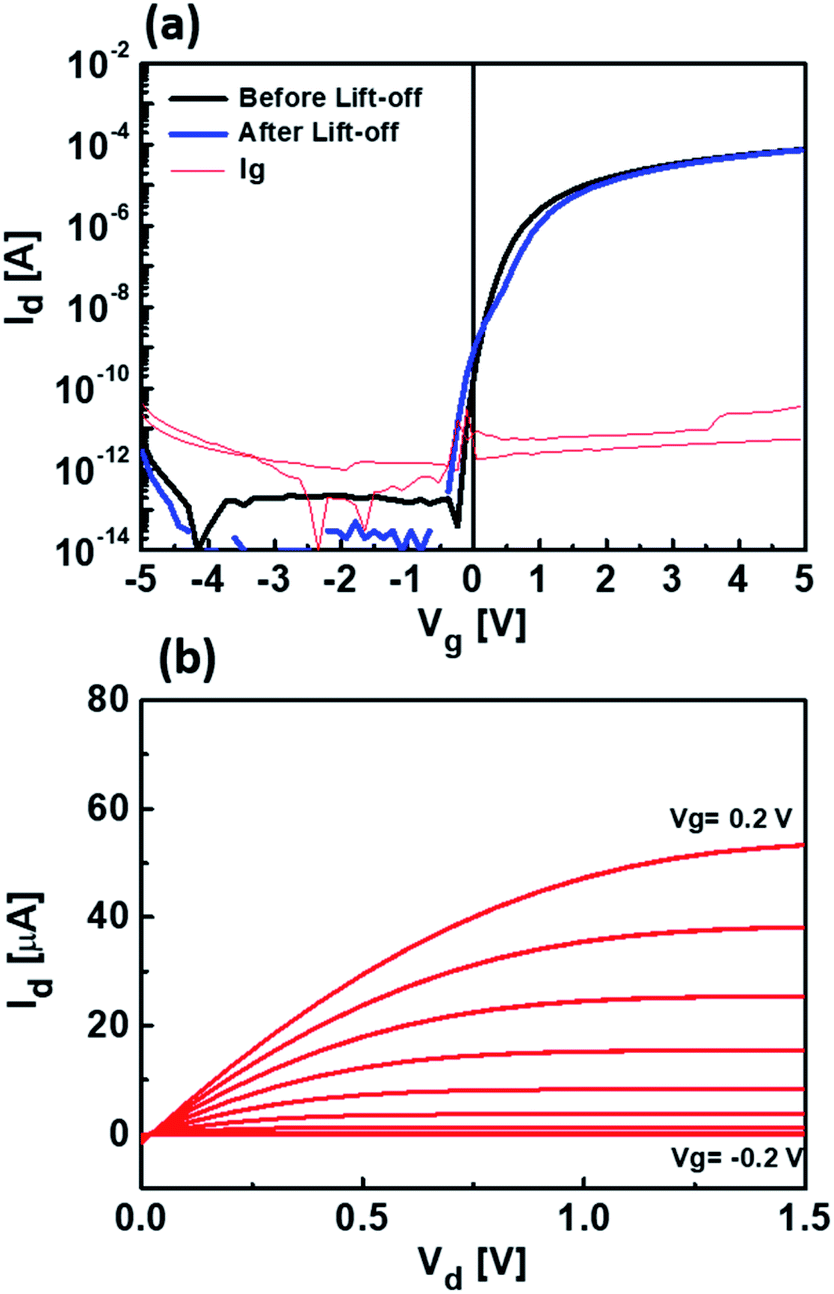 | ||
| Fig. 3 (a) Transfer characteristics of a-IGZO with w/l = 2560/20, before and after LLO. (b) Output characteristics of a-IGZO TFT for top gate voltages varying from −0.2 to 0.2 V. | ||
Transfer curves were also measured after LLO procedure. We found that, compared to the devices on the rigid substrate, the subthreshold swing and hysteresis of the flexible substrate devices were slightly larger. This should be due to the mechanical stress accumulated on the semiconductor layer during the delamination process. However, the two curves are not much different overall, so we expect that the sensor based on PI supported TFTs can still show a high performance as the sensor on the rigid substrate. The experimental data below, unless otherwise specified, are taken from the sensors on a flexible substrate.
We have also evaluated the performance of TFT outside the electromagnetically isolated environment since the semiconducting material is very sensitive to the surrounding environment. As shown in Fig. S4,† the transfer curve did not change much, except that the current in the off-state increases to 10−10 A order due to the influence of ambient noise. But this increment would not give a big impact on the sensor, since the current with a level of 10−10 A is still much smaller than the on-state current of the TFT.
Fig. 3b shows the output characteristics of the flexible oxide TFT. The gate voltage was applied from −0.2 V to 0.2 V in step of 0.04 V, and the drain voltage was swept from 0 to 1.5 V. Then, drain voltage was set to 0.1 V during sensor operation, which allows the TFT to work in a linear region so that the voltage signal from the piezoelectric film could take full advantages of the TFT.
Sensor performance
By stacking the piezoelectric capacitor on top of the TFT component, the proposed pressure sensor was fabricated. Owing to the strong electrostatic effect, the stretched film could achieve adhesive-free coverage. Nevertheless, the excessive static charge can also have a huge impact on the electrical properties of the TFT. Fig. 4a shows that the sensor's response to pressure is very stable when the device is properly shielded, but continues to shift down when the control gate is not properly grounded. The magnitude of the pressure was 8 kPa, the loading speed was 50 mm min−1, and the Vsd of the TFT was fixed at 0.1 V. Without proper shielding, the static electricity of the PVDF film can be easily affected, which in turn leads to unstable potential of the TFT gate. To study the effect of the external environment on the device, we tried to add a piece of debris to the test environment and evaluated the change in the TFT drain current (Fig. S5a and b†). By adjusting the distance between the debris and the device, whether the adjustment speed is fast or slow, the TFT drain current will show the corresponding change (Fig. S5c†). In addition, when an interference voltage was applied to an additional probe that does not have any contact with the device, the TFT drain current was still affected. Fig. 4b shows the drain current variation when a sweep voltage (−1 V to 1 V) was applied to an additional probe. The red curve shows the drain current output of the unshielded sensor throughout the voltage sweep. Even if no pressure is applied to the sensor, the response current still showed continuous variation with the interference voltage. Then, as shown in the black curve, the sensor was tapped five times during the voltage application, and each tap could be clearly distinguished. However, the current level of each tap differs from each other, indicates that the sensor without shielding structure would show a large error in practical application when integrated into the circuit. In addition, both curves show a huge hysteresis during the voltage sweep. This phenomenon again illustrates the effect of static electricity on the polymer film when the device is not shielded. In order to eliminate the above adverse effects, we propose to metallize the surface of the piezoelectric film and ground it to eliminate the interference of static electricity in the test environment.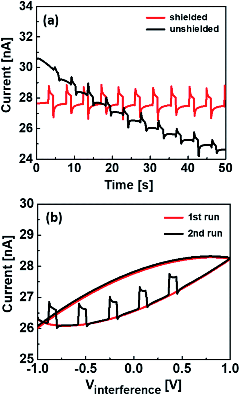 | ||
| Fig. 4 (a) The pressure sensor is stable when properly shielded. (b) Current response with interference voltage applied. There are no taps on the first run, and 5 taps on the sensor during the second run. | ||
Fig. 5 shows the current response to different pressures loaded on the sensor. As we have discussed in the previous section, when pressures are loaded on the piezoelectric film, charges would accumulate on the TFT gate electrode. Therefore, the gate potential of the TFT can be changed even if no external voltage is applied, which further leads to a variation in the drain current. Fig. 5a shows the drain current when sequential pressures (2 kPa, 4 kPa, 8 kPa, 17 kPa, 35 kPa, and 75 kPa) were imposed by the pressure test stand. The purpose of this study is to explore the feasibility of applying pressure sensors to touch screens. So, we didn't select a force gauge with a very wide pressure range. In this study, the maximum test pressure was set at 75 kPa. This pressure range of the force gauge is wide enough to cover the touch pressure, but is not suitable for the high-pressure limit detection. Each pressure was tested 10 times at a speed of 50 mm min−1, and the average current value for each pressure level was calculated. We have also labeled the error bar on each test point based on the actual data drift. We found that as the pressure increases, the value of the drain current increases. This is consistent with the voltage measurement results of piezoelectric films under pressure. Due to the use of piezoelectric materials, the sensor in this study exhibits better linearity over a wide range of pressures compared to other types of pressure sensors.41 According to the piezoelectric formula: Q = d33F (where Q is the charge from the aligned dipoles, d33 is the piezoelectric coefficient of PVDF, and F is the touch force applied to the PVDF film), the voltage developed when the piezoelectric material is pressed should increase linearly with the increase of external force. However, as the pressure increases, the offset of the drain current gradually increases and finally reaches saturation around 40 kPa. This result shows that the saturation behavior may be caused by the deformation limit of the PVDF layer under this pressure. Changing the piezoelectric material, layer thickness, and other ways to take the strain of the piezoelectric film saturated at greater pressure, may improve the detection limit of the sensing.
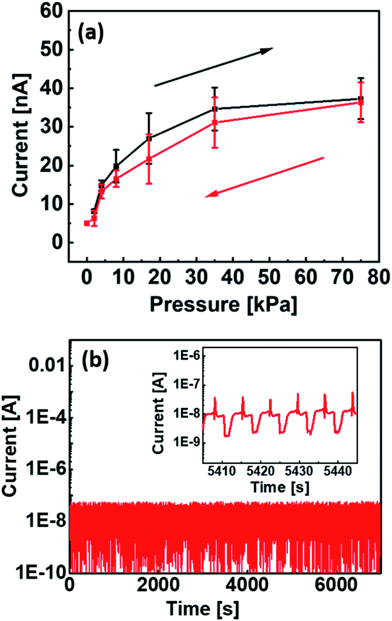 | ||
| Fig. 5 (a) Current response with sequential pressures applied to the sensor. (b) The durability test under a pressure of 75 kPa. | ||
Besides, to verify that the performance of the sensor is consistent, we have also recorded the drain current result by applying pressures in decreasing sequence order. Since the pressure applicator cannot achieve the required pressure very precisely, the curve is slightly shifted from the above results. However, the magnitude of the current measured through the two processes is still very close. This result indicates that regardless of the pressure loading sequence, the sensing performance of the sensor remains relatively consistent. The sensor described in this study is basically based on a piezoelectric pressure sensor. Different from the widely studied capacitive or piezoresistive pressure sensors, the pressure-sensitive body-material does not show a significant deformation under external stress. Instead, according to the piezoelectric principle, an electric potential will be formed across the film when it is subjected to an external force. As long as the external stress is within the normal range, that is, the piezoelectric film is not damaged, then the pressure sensor is stable.
As shown in Fig. S6,† a high-speed loading test of 200 mm min−1 has also been carried out. Since the piezoelectric materials are capable of generating higher voltages under high frequency pressure, we inferred that a larger induced current can be measured when the sensor is pressed in a high speed. The experimental results are consistent with the speculation. However, due to the flexibility of the device, a large amount of frictional static electricity was generated when the pressing tip contacts the device. Therefore, the consistency of the sensor output is not so ideal.
To study the reliability of the sensor, we loaded repeated 75 kPa pressures to the sensor using a test stand while recording the sensor output values throughout the test (Fig. 5b). As we have explained in the above, due to the effective shielding of the control gate, both the reference current and the response current remain constant throughout the entire 1000 repeated loading–unloading cycles. However, Fig. 5b shows that there are many points whose values are less than 10−9 A. It is clear from the inset that the current level can return to its initial value immediately when the pressure is released. In fact, these numerical anomalies actually stem from the unloading process of the pressure. When the speed of the pressure unloading is fast, a large negative voltage will be generated in the piezoelectric film in a moment. As a result, the output current of the sensor will be less than 10−9 A in a very short time. By carefully examining the raw data, we found that the number of points with these numerical anomalies is actually very small. But these points are conspicuous in the figure because they are recognized by the graphics software as important data and deliberately displayed on the figure. The endurance cycle test indicates that the sensor output current has a strong correlation with the loading and unloading of pressure, and the reproducibility of the current response at constant load is very high.
Conclusions
In conclusion, we have presented a highly-stable flexible pressure sensor. The sensor was fabricated by stacking a stretched piezoelectric polymer film on high mobility a-IGZO TFTs. The PVDF film shows a high β-phase crystallinity, and the a-IGZO TFT shows excellent semiconductor properties for constructing pressure sensors. Our study demonstrated that grounding the control gate will effectively shield external interference to the sensor and stabilize the signal. The low-voltage driving pressure sensor is able to detect different pressure levels in the pressure range of 0 to 75 kPa. More importantly, the sensor has excellent linearity over the wide pressure range and low measurement variation between imposing and releasing pressure. A high reproducibility of the current response was also showed by the sensor under 1000 cycles of the endurance test. Based on the above results, pressure sensors based on piezoelectric materials and TFTs have great potential for future touch screens. The ease of manufacturing flexible sensors makes low-cost preparation possible, and this method will be an excellent solution for next-generation touch screens.Conflicts of interest
There are no conflicts to declare.Acknowledgements
This work was supported by LG Display Co., Ltd., Nano Material Technology Development Program through the National Research Foundation of Korea(NRF) funded by the Ministry of Science, ICT and Future Planning (2016M3A7B4905609), and the Youth Research Fund of Liaoning University (LDQN202009).References
- T. Q. Trung and N. E. Lee, Adv. Mater., 2016, 28, 4338–4372 CrossRef CAS PubMed.
- Y. P. Zang, D. Z. Huang, C. A. Di and D. B. Zhu, Adv. Mater., 2016, 28, 4549–4555 CrossRef CAS PubMed.
- M. Cao, J. Su, S. Fan, H. Qiu, D. Su and L. Li, Chem. Eng. J., 2021, 406, 126777 CrossRef CAS.
- Z. Tang, S. Jia, C. Zhou and B. Li, ACS Appl. Mater. Interfaces, 2020, 12, 28669–28680 CrossRef CAS PubMed.
- W. Li, X. Jin, X. Han, Y. Li, W. Wang, T. Lin and Z. Zhu, ACS Appl. Mater. Interfaces, 2021, 13, 19211–19220 CrossRef CAS PubMed.
- G. Yang, M. Z. Tian, P. Huang, Y. F. Fu, Y. Q. Li, Y. Q. Fu, X. Q. Wang, Y. Li, N. Hu and S. Y. Fu, Carbon, 2021, 173, 736–743 CrossRef CAS.
- C. Xie, M. Zhang, W. Du, C. J. Zhou, Y. Xiao, S. Zhang and M. S. Chan, RSC Adv., 2020, 10, 33558–33565 RSC.
- T. Someya, T. Sekitani, S. Iba, Y. Kato, H. Kawaguchi and T. Sakurai, Proc. Natl. Acad. Sci. U.S.A., 2004, 101, 9966–9970 CrossRef CAS PubMed.
- B. C. K. Tee, A. Chortos, R. R. Dunn, G. Schwartz, E. Eason and Z. A. Bao, Adv. Funct. Mater., 2014, 24, 5427–5434 CrossRef CAS.
- Y. S. Luo, J. Y. Shao, S. R. Chen, X. L. Chen, H. M. Tian, X. M. Li, L. Wang, D. R. Wang and B. H. Lu, ACS Appl. Mater. Interfaces, 2019, 11, 17796–17803 CrossRef CAS PubMed.
- T. Li, H. Luo, L. Qin, X. W. Wang, Z. P. Xiong, H. Y. Ding, Y. Gu, Z. Liu and T. Zhang, Small, 2016, 12, 5042–5048 CrossRef CAS PubMed.
- X. W. Wang, Y. Gu, Z. P. Xiong, Z. Cui and T. Zhang, Adv. Mater., 2014, 26, 1336–1342 CrossRef CAS PubMed.
- T. Jin, Y. Pan, G.-J. Jeon, H.-I. Yeom, S. Zhang, K.-W. Paik and S.-H. K. Park, ACS Appl. Mater. Interfaces, 2020, 12, 13348–13359 CrossRef CAS PubMed.
- G.-J. Jeon, H.-I. Yeom, T. Jin, J. Kim, J. Yang and S.-H. K. Park, J. Mater. Chem. C, 2020, 8, 4271–4278 RSC.
- G. Schwartz, B. C. K. Tee, J. G. Mei, A. L. Appleton, D. H. Kim, H. L. Wang and Z. N. Bao, Nat. Commun., 2013, 4, 1859 CrossRef PubMed.
- D. Kwon, T. I. Lee, J. Shim, S. Ryu, M. S. Kim, S. Kim, T. S. Kim and I. Park, ACS Appl. Mater. Interfaces, 2016, 8, 16922–16931 CrossRef CAS PubMed.
- S. Pyo, J. Choi and J. Kim, Adv. Electron. Mater., 2018, 4, 1700427 CrossRef.
- G. T. Hwang, H. Park, J. H. Lee, S. Oh, K. I. Park, M. Byun, H. Park, G. Ahn, C. K. Jeong, K. No, H. Kwon, S. G. Lee, B. Joung and K. J. Lee, Adv. Mater., 2014, 26, 4880–4887 CrossRef CAS PubMed.
- X. S. Niu, W. Jia, S. Qian, J. Zhu, J. Zhang, X. J. Hou, J. L. Mu, W. P. Geng, J. D. Cho, J. He and X. J. Chou, ACS Sustainable Chem. Eng., 2019, 7, 979–985 CrossRef CAS.
- M. Sung, K. Shin and W. Moon, Sens. Actuators, A, 2015, 233, 557–568 CrossRef CAS.
- S. Gee, B. Johnson and A. L. Smith, J. Membr. Sci., 2018, 563, 804–812 CrossRef CAS.
- X. L. Chen, J. Y. Shao, X. M. Li and H. M. Tian, IEEE Trans. Nanotechnol., 2016, 15, 295–302 CAS.
- H. Paik, Y. Y. Choi, S. Hong and K. No, Sci. Rep., 2015, 5, 13209 CrossRef PubMed.
- S. H. Bae, O. Kahya, B. K. Sharma, J. Kwon, H. J. Cho, B. Ozyilmaz and J. H. Ahn, ACS Nano, 2013, 7, 3130–3138 CrossRef CAS PubMed.
- Y. Tsuji, H. Sakai, L. R. Feng, X. J. Guo and H. Murata, Appl. Phys. Express, 2017, 10, 021601 CrossRef.
- C. Dagdeviren, Y. W. Su, P. Joe, R. Yona, Y. H. Liu, Y. S. Kim, Y. A. Huang, A. R. Damadoran, J. Xia, L. W. Martin, Y. G. Huang and J. A. Rogers, Nat. Commun., 2014, 5, 4496 CrossRef CAS PubMed.
- S.-I. Cho, J. B. Ko, S. H. Lee, J. Kim and S.-H. K. Park, J. Alloys Compd., 2022, 893, 162308 CrossRef CAS.
- G.-J. Jeon, J. Yang, S. H. Lee, W. Jeong and S. H. K. Park, IEEE Electron Device Lett., 2021, 42, 363–366 CAS.
- D. Geng, S. Han, H. Seo, M. Mativenga and J. Jang, IEEE Sens. J., 2017, 17, 585–586 Search PubMed.
- A. Pecora, L. Maiolo, F. Maita and A. Minotti, Sens. Actuators, A, 2012, 185, 39–43 CrossRef CAS.
- W. Park, J. H. Yang, C. G. Kang, Y. G. Lee, H. J. Hwang, C. Cho, S. K. Lim, S. C. Kang, W. K. Hong, S. K. Lee, S. Lee and B. H. Lee, Nanotechnology, 2013, 24, 475501 CrossRef PubMed.
- J. Bae, B. S. Ma, G. Jeon, W. Jeong, C. H. Je, T. S. Kim and S. H. K. Park, IEEE Electron Device Lett., 2019, 40, 1760–1763 CAS.
- D. Sengupta, A. G. P. Kottapalli, S. H. Chen, J. M. Miao, C. Y. Kwok, M. S. Triantafyllou, M. E. Warkiani and M. Asadnia, AIP Adv., 2017, 7, 105205 CrossRef.
- J. H. Bae and S. H. Chang, Compos. Struct., 2015, 131, 1090–1098 CrossRef.
- G. Wang, T. Liu, X. C. Sun, P. Li, Y. S. Xu, J. G. Hua, Y. H. Yu, S. X. Li, Y. Z. Dai, X. Y. Song, C. Lv and H. Xia, Sens. Actuators, A, 2018, 280, 319–325 CrossRef CAS.
- L. Li, M. Zhang, M. Rong and W. Ruan, RSC Adv., 2014, 4, 3938 RSC.
- Y. Ting, Suprapto, C.-W. Chiu and H. Gunawan, J. Appl. Polym. Sci., 2018, 135, 46677 CrossRef.
- X. M. Cai, T. P. Lei, D. H. Sun and L. W. Lin, RSC Adv., 2017, 7, 15382–15389 RSC.
- Z. H. Liu, C. T. Pan, C. Y. Su, L. W. Lin, Y. J. Chen and J. S. Tsai, Sens. Actuators, A, 2014, 211, 78–88 CrossRef CAS.
- Y. Nam, H. O. Kim, S. H. Cho and S. H. K. Park, RSC Adv., 2018, 8, 5622–5628 RSC.
- A. Chhetry, P. S. Das, H. Yoon and J. Y. Park, Org. Electron., 2018, 62, 581–590 CrossRef CAS.
Footnote |
| † Electronic supplementary information (ESI) available: Fig. S1: transfer characteristics of a-IGZO TFTs with various active widths; Fig. S2: measurement setup for the pressure sensor; Fig. S3: voltage generated across the piezoelectric film when pressure is applied; Fig. S4: transfer characteristics of a-IGZO TFT measured outside the electromagnetically isolated box; Fig. S5: photo images of a piece of debris (a) away and (b) close to the sensor; (c) current response with a piece of debris gradually approaches, slowly approaches, and rapidly approaches to the sensor; Fig. S6: current response with high-speed pressures applied to the sensor. See https://doi.org/10.1039/d2ra02613a |
| This journal is © The Royal Society of Chemistry 2022 |