
 Open Access Article
 This Open Access Article is licensed under a Creative Commons Attribution-Non Commercial 3.0 Unported Licence
Micro-nano hierarchical pillar array structures prepared on curved surfaces by nanoimprinting using flexible molds from anodic porous alumina and their application to superhydrophobic surfaces
Takashi Yanagishita *,
Takchiu Sou and
Hideki Masuda
*,
Takchiu Sou and
Hideki Masuda
Department of Applied Chemistry, Tokyo Metropolitan University, 1-1 Minamiosawa, Hachioji, Tokyo 192-0397, Japan. E-mail: yanagish@tmu.ac.jp
First published on 13th July 2022
Abstract
Flexible molds with micro-nano hierarchical structures on the surface were fabricated by a two-step template process using anodic porous alumina as a starting material. The obtained flexible molds could be used to form micro-nano hierarchical pillar arrays on the surface of glass tubes and convex lenses by photo-nanoimprinting. The contact angle characteristics of the surfaces with hierarchical pillar arrays were measured, and it was confirmed that they exhibit superhydrophobic properties with a water-droplet contact angle exceeding 150°. The flexible molds obtained in this study can be used repeatedly and efficiently to form micro-nano hierarchical surfaces with superhydrophobic properties on the surfaces of substrates with various curvatures.
Introduction
Nanostructured surfaces exhibit various functions depending on their surface morphology.1–4 Nanoimprinting is an effective method for preparing various functional nanostructured surfaces, such as antireflective, water-repellent, and antibacterial surfaces, because it enables the efficient patterning of the controlled fine structures on the substrate surface.5–14 Nanoimprinting molds are usually fabricated by a combination of electron beam lithography and dry etching.15,16 However, these methods have some problems, such as the difficulty in fabricating molds with large-area patterns and high-aspect-ratio structures. We have been investigating the formation of ordered fine patterns by nanoimprinting using an anodic porous alumina mold obtained by the anodization of Al in an appropriate acidic electrolyte.17–19 Anodic porous alumina is characterized by its ability to effectively form ordered nanohole array structures with high aspect ratios, in addition to large areas.20 Nanoimprinting using anodic porous alumina as a mold is suitable for preparing structures with high aspect ratios and large sample sizes.In the present work, we have expanded the nanoimprinting process using anodic porous alumina molds to the preparation of micro-nano hierarchical structures on curved surfaces. The preparation of fine patterns on curved surfaces is important for the functionalization of the surfaces. As one possible process for the preparation of the fine patterns on the curved surfaces by nanoimprinting, we have demonstrated the nanoimprinting process by using a mold prepared by the anodization of an Al substrate with a given curved surface.21,22 The problem with this process is that applicable samples are limited to substrates with curvatures identical to the mold curved surface. To overcome this problem, we have introduced flexible molds originating from the anodic porous alumina used as a starting structure. The use of a flexible mold composed of polydimethylsiloxane (PDMS) has been reported in the preparation of fine patterns of polymers on various curved surfaces.23–25 Since the flexible mold can deform itself to follow the surface shape of the substrate, it is possible to form fine patterns on various curved surfaces using a single mold. In contrast, the sample areas and aspect ratios of the obtained structures were limited in the previously reported process based on mold preparation processes. In addition, to the best of our knowledge, there are no reports of the formation of micro-nano hierarchical structures, which are effective for superhydrophobic surfaces,26 by nanoimprinting using flexible molds. Here, we describe the preparation of high-aspect-ratio hierarchical pillar arrays on curved surfaces by nanoimprinting using a flexible mold fabricated from anodic porous alumina and their application to superhydrophobic surfaces for the first time. In the present work, the flexible molds with hierarchical structures were prepared by a two-step template process using anodic porous alumina as a starting material. First, anodic porous alumina with hierarchical structures was prepared by an integrated process composed of anodization and selective patterning.27,28 Next, polymer negatives of anodic porous alumina with the hierarchical structures were formed, and finally, the flexible mold was obtained by molding using the polymer negative as a mold. This process can effectively form high-aspect-ratio micropillars with nanopillar arrays at their tips on curved surfaces. Although the formation of hierarchical structures by nanoimprinting has been reported, a method that can form hierarchical pillar arrays with aspect ratios exceeding 5 on curved surfaces has not been reported. Surfaces with hierarchical pillar arrays formed with high aspect ratios are considered to trap a layer of air between water droplets and the substrate surface more easily than surfaces with hierarchical structures formed with low aspect ratios. According to the Cassie–Baxter model, a surface with air trapped between water droplets and the substrate surface functions as an excellent water-repellent surface.29 Therefore, this process is expected to be an efficient method for making curved substrate surfaces superhydrophobic. In addition, this process can form a hierarchical pillar array structure with a high aspect ratio, similar to the hierarchical structure found on the sole of a gecko foot, and is expected to be used for preparing structural adhesive surfaces on curved substrates.30
Experimental
Fig. 1 shows a schematic diagram of the process of preparing a flexible mold with a micro-nano hierarchical structure on the surface and nanoimprinting using the obtained flexible mold. In this study, the ordered anodic porous alumina used as a starting material was prepared by two-step anodization, as reported previously.31 An Al sheet (99.99% purity) was polished electrochemically in a mixture of perchloric acid and ethanol (1![[thin space (1/6-em)]](https://www.rsc.org/images/entities/char_2009.gif) :4 in volume ratio) at 0.1 mA cm−2 for 4 min to achieve a mirror surface. The electropolished Al sheet was anodized in 0.1 M phosphoric acid under a constant voltage of 195 V at 0 °C for 16 h to obtain an ordered hole arrangement. The oxide layer formed by the first anodization was dissolved selectively in a mixture of 1.8 wt% chromic acid and 6 wt% phosphoric acid, and then anodized again for 2 h under the same conditions to prepare the ordered anodic porous alumina with an interhole distance of 500 nm and a film thickness of 8 μm. After anodization, a resist mask with micropatterns was formed on the surface of the anodic porous alumina by a stamping process. For the formation of the resist mask, a polydimethylsiloxane (PDMS) stamp with a square pattern of micrometer-size protrusions on the surface prepared using the prepolymer (TSE3450, Momentive Performance Materials Inc.) was used. The surface pattern of the PDMS stamp was fabricated by a molding process using patterns formed by electron beam lithography as a starting structure. The PDMS stamp was immersed in a toluene solution containing 0.2 wt% polychloroprene (Nisshin EM Co., Japan) and pulled up at a constant rate of 1 mm s−1 to form a polychloroprene thin film in the recesses of the stamp surface. In this method, a polychloroprene thin film is formed on the surface of the PDMS stamp as the dip-coated solution dries and solidifies. The thickness of the polychloroprene film formed on the stamp surface can be controlled by adjusting the concentration of the solution and the pull-up speed of the stamp. By pressing the stamp onto the anodic porous alumina, a resist mask with a micrometer-size aperture pattern corresponding to the surface structure of the stamp was transferred. This is because the polychloroprene film on the stamp surface adheres better to anodic porous alumina than to PDMS, and the film can be transferred by pressing the stamp against the anodic porous alumina. The sample with the resist mask was immersed in a mixture of 1.8 wt% chromic acid and 6 wt% phosphoric acid at 50 °C for 1 h to dissolve the alumina layer from the resist aperture and obtain a micrometer-size cavity array with exposed Al at the bottom of the cavities. Although acids other than a mixture of chromic acid and phosphoric acid can be used for the selective dissolution of the alumina layer, the etchant we used does not dissolve Al; thus, so etching can be stopped when residual Al is exposed. The sample was anodized again for 1 h in 0.1 M phosphoric acid at 195 V to obtain a hierarchical structure with nanohole arrays at the bottom of the microcavities. To increase the hole size of the porous alumina formed at the bottom of the microcavities, etching was performed in 10 wt% phosphoric acid at 30 °C for 1 h. After etching, the sample was treated with fluoroalkylsilane (Optool DSX, Daikin Industries, Ltd., Japan) as a mold release agent. A micro-nano hierarchical pillar array was obtained on a polyethylene terephthalate (PET) sheet by photo-nanoimprinting using anodic porous alumina as a mold and a photocurable monomer (PAK-02, Toyo Gosei Co., Japan).
:4 in volume ratio) at 0.1 mA cm−2 for 4 min to achieve a mirror surface. The electropolished Al sheet was anodized in 0.1 M phosphoric acid under a constant voltage of 195 V at 0 °C for 16 h to obtain an ordered hole arrangement. The oxide layer formed by the first anodization was dissolved selectively in a mixture of 1.8 wt% chromic acid and 6 wt% phosphoric acid, and then anodized again for 2 h under the same conditions to prepare the ordered anodic porous alumina with an interhole distance of 500 nm and a film thickness of 8 μm. After anodization, a resist mask with micropatterns was formed on the surface of the anodic porous alumina by a stamping process. For the formation of the resist mask, a polydimethylsiloxane (PDMS) stamp with a square pattern of micrometer-size protrusions on the surface prepared using the prepolymer (TSE3450, Momentive Performance Materials Inc.) was used. The surface pattern of the PDMS stamp was fabricated by a molding process using patterns formed by electron beam lithography as a starting structure. The PDMS stamp was immersed in a toluene solution containing 0.2 wt% polychloroprene (Nisshin EM Co., Japan) and pulled up at a constant rate of 1 mm s−1 to form a polychloroprene thin film in the recesses of the stamp surface. In this method, a polychloroprene thin film is formed on the surface of the PDMS stamp as the dip-coated solution dries and solidifies. The thickness of the polychloroprene film formed on the stamp surface can be controlled by adjusting the concentration of the solution and the pull-up speed of the stamp. By pressing the stamp onto the anodic porous alumina, a resist mask with a micrometer-size aperture pattern corresponding to the surface structure of the stamp was transferred. This is because the polychloroprene film on the stamp surface adheres better to anodic porous alumina than to PDMS, and the film can be transferred by pressing the stamp against the anodic porous alumina. The sample with the resist mask was immersed in a mixture of 1.8 wt% chromic acid and 6 wt% phosphoric acid at 50 °C for 1 h to dissolve the alumina layer from the resist aperture and obtain a micrometer-size cavity array with exposed Al at the bottom of the cavities. Although acids other than a mixture of chromic acid and phosphoric acid can be used for the selective dissolution of the alumina layer, the etchant we used does not dissolve Al; thus, so etching can be stopped when residual Al is exposed. The sample was anodized again for 1 h in 0.1 M phosphoric acid at 195 V to obtain a hierarchical structure with nanohole arrays at the bottom of the microcavities. To increase the hole size of the porous alumina formed at the bottom of the microcavities, etching was performed in 10 wt% phosphoric acid at 30 °C for 1 h. After etching, the sample was treated with fluoroalkylsilane (Optool DSX, Daikin Industries, Ltd., Japan) as a mold release agent. A micro-nano hierarchical pillar array was obtained on a polyethylene terephthalate (PET) sheet by photo-nanoimprinting using anodic porous alumina as a mold and a photocurable monomer (PAK-02, Toyo Gosei Co., Japan).
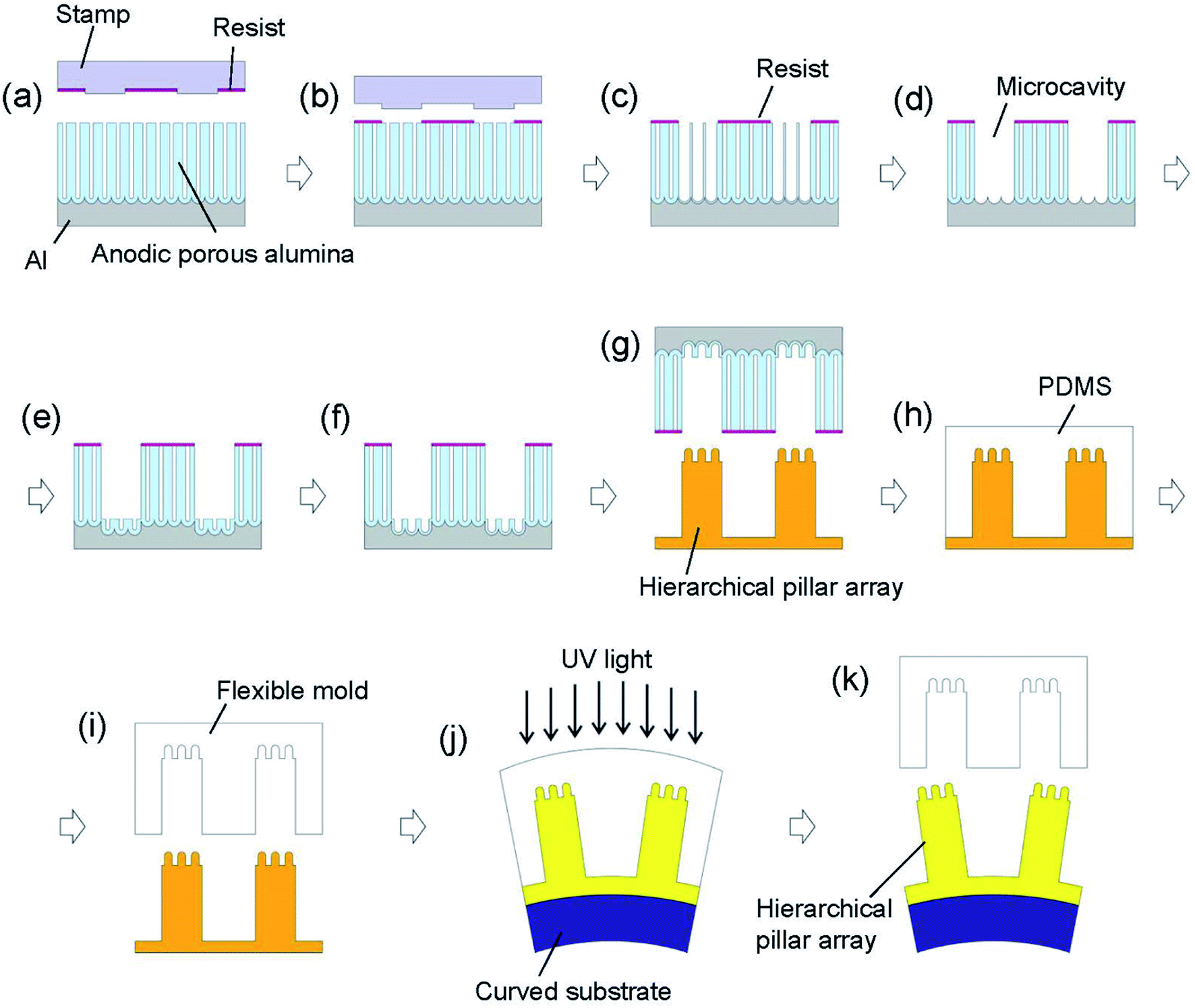 | ||
| Fig. 1 Schematic diagram of experimental process: (a) anodization, (b) formation of resist mask, (c) selective etching, (d) selective dissolution of alumina layer, (e) re-anodization, (f) enlargement of nanohole, (g) formation of hierarchical pillar array, (h) pouring of prepolymer, (i) detachment of flexible mold, (j) photo-nanoimprinting, and (k) peeling of flexible mold. | ||
The flexible molds were fabricated by a template process using the micro-nano hierarchical pillar arrays obtained using anodic porous alumina. A PDMS prepolymer (SIM-260, Shin-Etsu Chemical Co., Japan), which is suitable for fine pattern molding, was poured into the hierarchical polymer pillar array, left to cure at 65 °C for 3 h, and then peeled off to obtain a flexible mold with micro-nano hierarchical structures formed on the surface. Before nanoimprinting using the flexible mold, the mold was treated with fluoroalkylsilane (Optool DSX, Daikin Industries, Ltd.) to form a release layer on the surface. The flexible mold was used to form micro-nano hierarchical patterns on surfaces with curvature by photo-nanoimprinting. The surfaces of the obtained samples were modified with fluoroalkylsilane (Optool DSX, Daikin Industries, Ltd.), and the contact angles with water droplets were evaluated. The geometrical structures of the obtained samples were also observed by scanning electron microscopy (SEM; JSM-7500F, JEOL).
Results and discussion
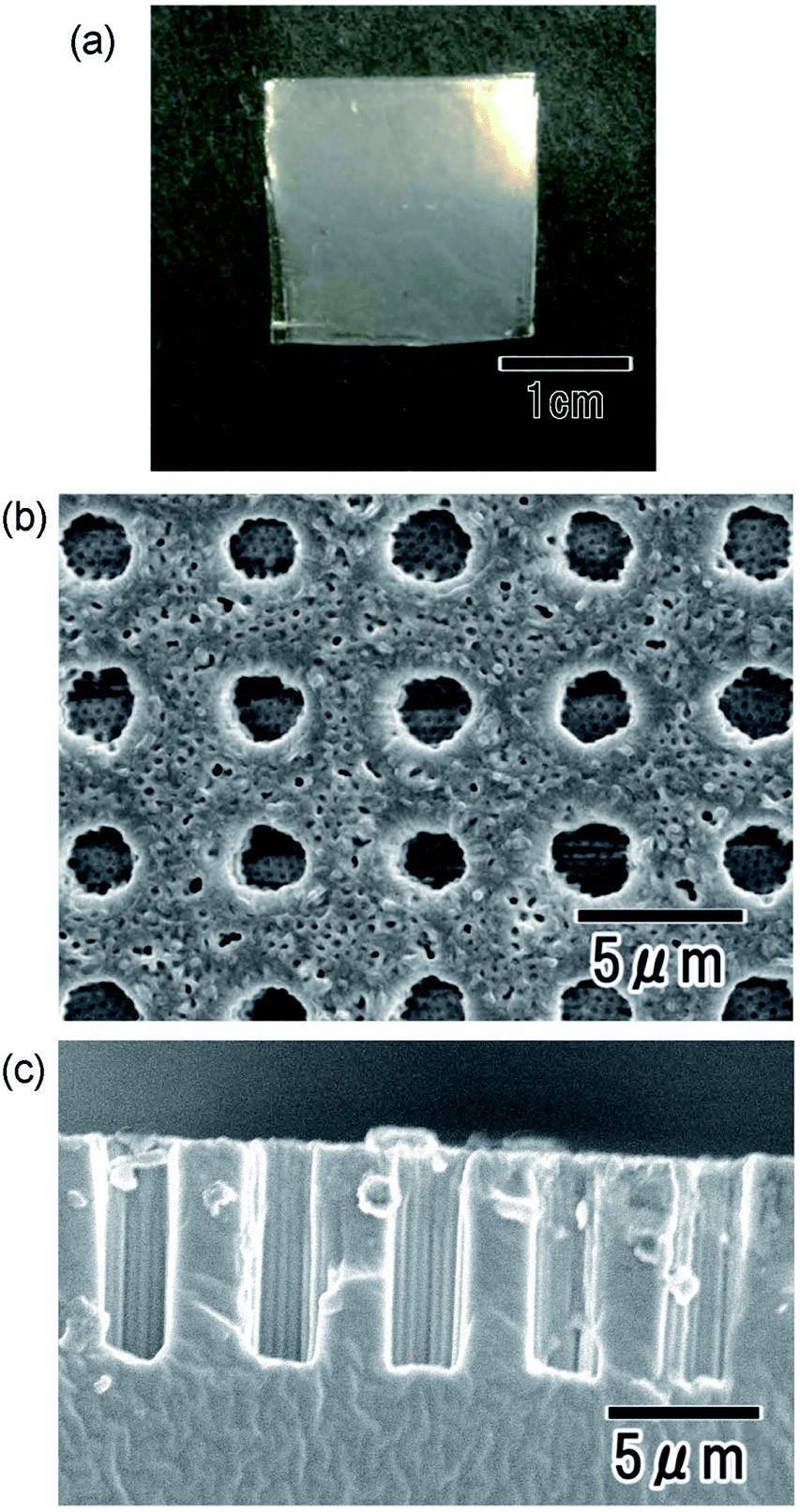
Fig. 2 shows surface and cross-sectional SEM images of anodic porous alumina with hierarchical structures. The SEM observation of the specimen was performed after the re-anodization of anodic porous alumina with a microcavity array. The low-magnification image of the surface in Fig. 2(a) shows a square lattice array of microcavities with a diameter of approximately 2 μm and a period of 5 μm. This shows good correspondence with the surface pattern of the stamp used for resist formation. From the cross-sectional SEM image shown in Fig. 2(b), it can be observed that the porous alumina layer in the resist aperture is completely dissolved to the bottom by selective etching. When anodic porous alumina is immersed in an etchant, the etchant penetrates to the bottom of the holes, causing the uniform dissolution of the hole walls from the top to the bottom of the holes and increasing the hole diameter. As etching continues, the hole walls dissolve and the holes coalesce, further dissolving the residue and exposing the residual Al substrate. If a resist mask is formed on anodic porous alumina prior to etching to cover some of the holes, as in this process, the etchant penetrates only inside the holes of the anodic porous alumina at the resist openings, and the hole walls are dissolved. This makes it possible to dissolve only the alumina layer at the resist opening selectively. This is an anisotropic etching process based on the hole array structure of anodic porous alumina. Any acid can be used for etching the alumina layer, but etching can be stopped when the Al substrate is exposed by using an etchant containing chromic acid. This is because when the Al substrate is exposed by etching, a passive film is formed on the Al surface by the effect of the chromic acid, and no further etching occurs. From Fig. 2(b), it can also be observed that a nanohole array structure is formed at the bottom of the microcavity by re-anodization. The depths of the microcavities and nanoholes in the obtained sample were 8 μm and 220 nm, respectively. The thickness of the resist mask formed on the stamp surface by dipcoating depends on the concentration of the polychloroprene solution and the pull-up speed. If a thick resist is formed by dip coating on the entire micropattern on the surface of the stamp, the resist pattern transferred to the porous alumina surface has no openings. On the other hand, if the resist film formed on the stamp surface is very thin, the holes of anodic porous alumina are not covered by the resist, and the etchant penetrates into all the holes during etching, resulting in dissolution over the entire sample surface. Therefore, to selectively dissolve anodic porous alumina by this process, it is important to control the thickness of the resist film formed on the stamp surface by dip coating.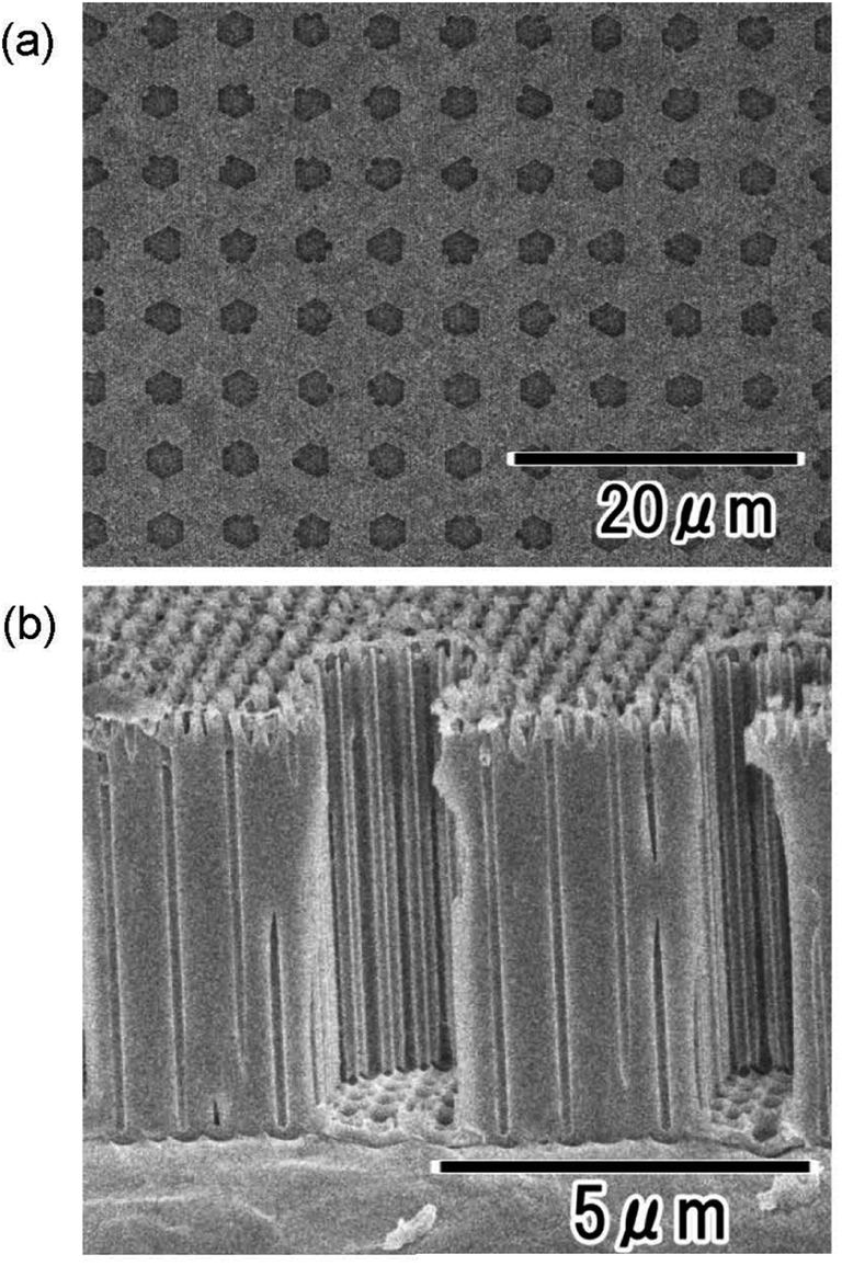 | ||
| Fig. 2 (a) Surface and (b) cross-sectional SEM images of anodic porous alumina with hierarchical structures. | ||
This process can produce anodic porous alumina with a hierarchical structure even when the interhole distance of anodic porous alumina is varied. Fig. 3 shows the results for micro-nano hierarchical structures fabricated from anodic porous alumina with interhole distances of 100, 200, and 300 nm as starting structures. The SEM images in Fig. 3 show that nanohole arrays with hole periods of 100, 200, and 300 nm are formed at the bottom of microholes with a diameter of 2 μm.
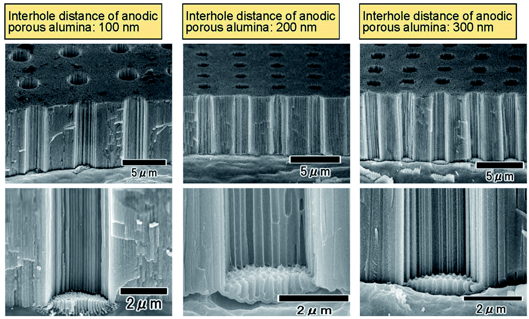 | ||
| Fig. 3 SEM images of micro-nano hierarchical structures fabricated from anodic porous alumina with interhole distances of 100, 200, and 300 nm as starting structures. The anodic porous alumina with an interhole period of 100 nm was formed by the anodization of Al in 0.3 M oxalic acid at 40 V and 17 °C for 60 min. The anodic porous alumina with an interhole period of 200 nm was formed by the anodization of Al in 0.05 M oxalic acid at 80 V and 0 °C for 60 min. The anodic porous alumina with an interhole period of 300 nm was performed by the anodization of Al in 0.05 M oxalic acid at 120 V and 0 °C for 60 min. | ||
Fig. 4 shows SEM images of a micro-nano hierarchical pillar array formed on a flat substrate using the anodic porous alumina shown in Fig. 2. The low- and high-magnification SEM images of the cross section in Fig. 4(a) and (b) show vertical hierarchical pillars of uniform diameter and height on the substrate. The height of the obtained hierarchical pillars was 8 μm, which corresponded to the depth of the microcavities in the anodic porous alumina used as the starting structure. The high-magnification SEM image of the upper part of the hierarchical pillars in Fig. 4(c) shows the nanopillar array formed at the tip of a micropillar. When nanoimprinting was performed using the anodic porous alumina master with a releasing layer on its surface, a defect-free hierarchical pillar array was formed over the entire surface of the sample.
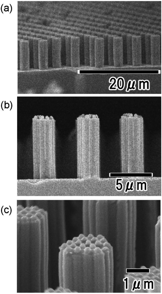 | ||
| Fig. 4 (a) and (b) Cross-sectional SEM images of hierarchical pillar arrays prepared from anodic porous alumina. (c) High-magnification SEM image of upper part of hierarchical pillars. | ||
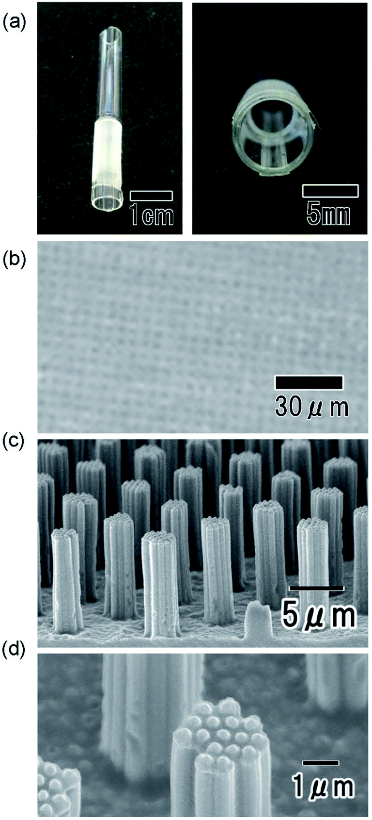
Fig. 5 shows the observation results of a flexible mold fabricated using the hierarchical pillar array shown in Fig. 4 as a template. The photograph in Fig. 5(a) confirms that a flexible mold with a size of 2 cm square was successfully formed. The surface SEM image in Fig. 5(b) shows a square lattice of microholes with a diameter of approximately 2 μm and a spacing of 5 μm. In addition, a nanohole array with an interhole distance of 500 nm was observed to be transferred at the bottom of the microcavities. The cross-sectional SEM image in Fig. 5(c) shows that the depth of the microcavities is 8 μm, confirming that the structure of porous alumina used as the starting structure is retained even after two transfer processes.
 | ||
| Fig. 5 (a) Photograph of flexible mold. (b) Surface and (c) cross-sectional SEM images of flexible mold. | ||
Fig. 6 shows the results of hierarchical pillar arrays formed on the surface of a glass tube with a diameter of 7 mm by photo-nanoimprinting using the flexible mold. Fig. 6(a) shows photographs of the glass tube after photo-nanoimprinting. It can be seen that the nanoimprinted area has turned white. This is due to light scattering in areas with hierarchical pillar arrays formed by nanoimprinting using the flexible mold. The flexible mold fabricated in this study deforms along with the shape of the substrate, making it possible to form a pattern on the entire surface of the glass tube. The optical microscopy image of the imprinted sample shown in Fig. 6(b) confirms that a square lattice of micropillars is formed over a large area. From the SEM images in Fig. 6(c) and (d), vertical micropillars with a nanopillar array at the tip were observed to form on the curved surface. The flexible mold could be detached from the substrate while deforming even during peeling, making it possible to form hierarchical pillars that maintained an upright structure on each curved surface.
 | ||
| Fig. 6 (a) Photographs of specimen after photo-nanoimprinting using flexible mold. (b) Optical microscopy image of specimen. (c) Low- and (d) high-magnification SEM images of hierarchical pillar array formed by photo-nanoimprinting using flexible mold. | ||
Fig. 7(a) shows the results of preparing hierarchical pillar arrays of different heights on a curved surface by photo-nanoimprinting using a flexible mold. Similar to the experimental results shown in Fig. 6, a glass tube with a diameter of 7 mm was used as the substrate for nanoimprinting. The surface structure of the flexible mold was controlled by varying the thickness of the porous alumina film used as the starting material. The SEM images in Fig. 7(a) show that the heights of the obtained hierarchical pillars were 5, 8, and 16 μm. Even in the case of the tallest pillar fabricated in this study (16 μm), it was possible to form pillar arrays on a curved surface while maintaining the upright structure. The SEM images in Fig. 7(b) show the results of controlling the height of the nanopillars at the tip of the micropillar. The height of the nanopillars was varied from 200 nm to 420 nm by varying the anodization time from 1 h to 2 h during the preparation of anodic porous alumina with a hierarchical structure. These results show that the geometrical structure of hierarchical pillar arrays formed on curved surfaces by photo-nanoimprinting using flexible molds can be controlled by changing the starting structure.
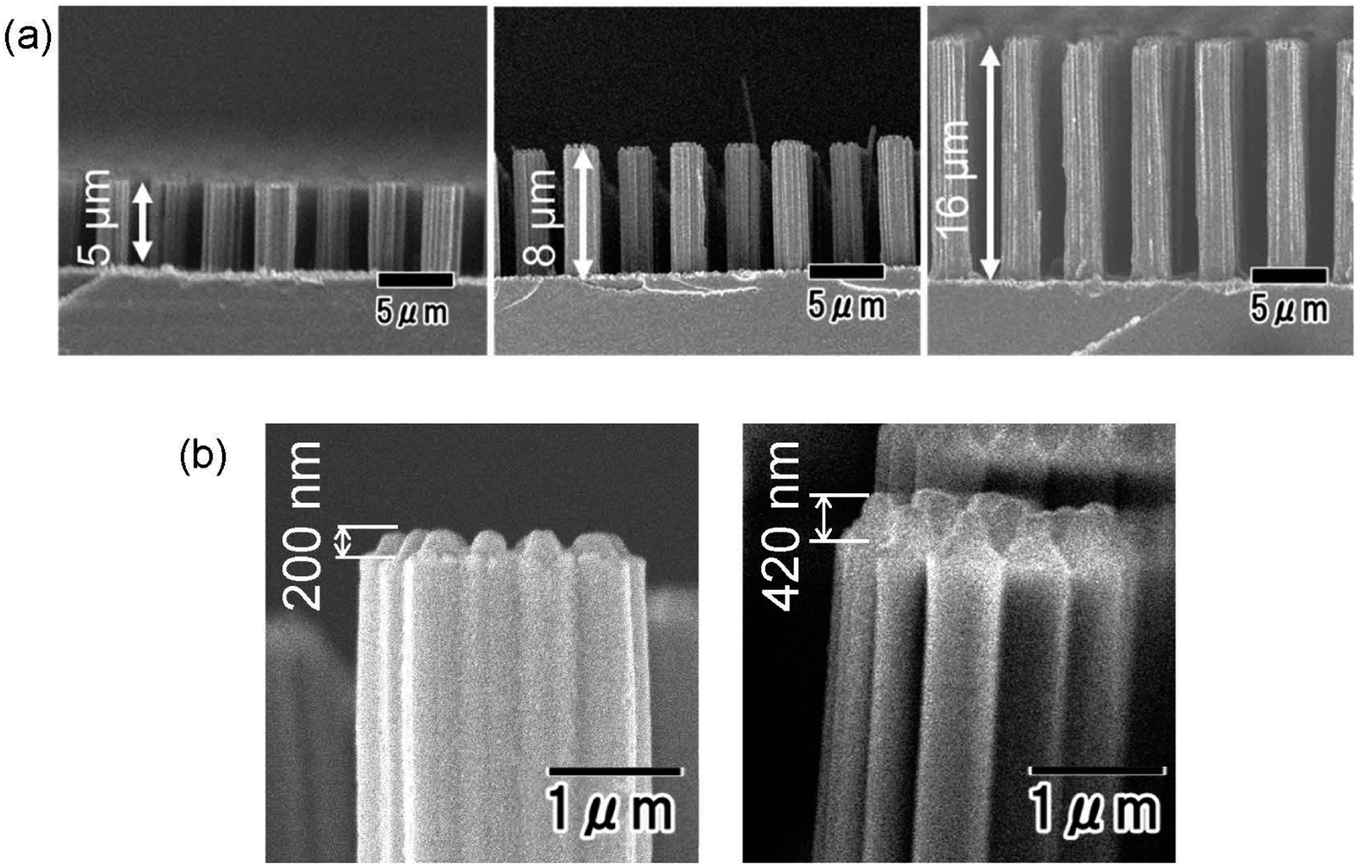 | ||
| Fig. 7 (a) SEM images of hierarchical pillar arrays with controlled micropillar height. (b) SEM images of hierarchical pillar arrays with controlled nanopillar height. | ||
Fig. 8 shows the results of micro-nano hierarchical pillar arrays formed by nanoimprinting using a flexible mold on convex lens surfaces with different curvature radii. From the photographs of the specimens, it can be seen that the entire surface of each spechimen is white, for all curvature radii of 52, 26, and 10 mm, indicating that the fine patterns were transferred. SEM observations of each sample also indicated that hierarchical pillar arrays were formed without defects on all of the curved surfaces of different curvature radii. These results indicate that the flexible molds fabricated in this study can be used to form hierarchical pillar arrays not only on two-dimensional curved surfaces, such as cylinders and tubes, but also on three-dimensional curved surfaces such as lenses. We believe this is because the flexible mold made of PDMS can not only deform flexibly but also stretch to follow the convex lens shape.
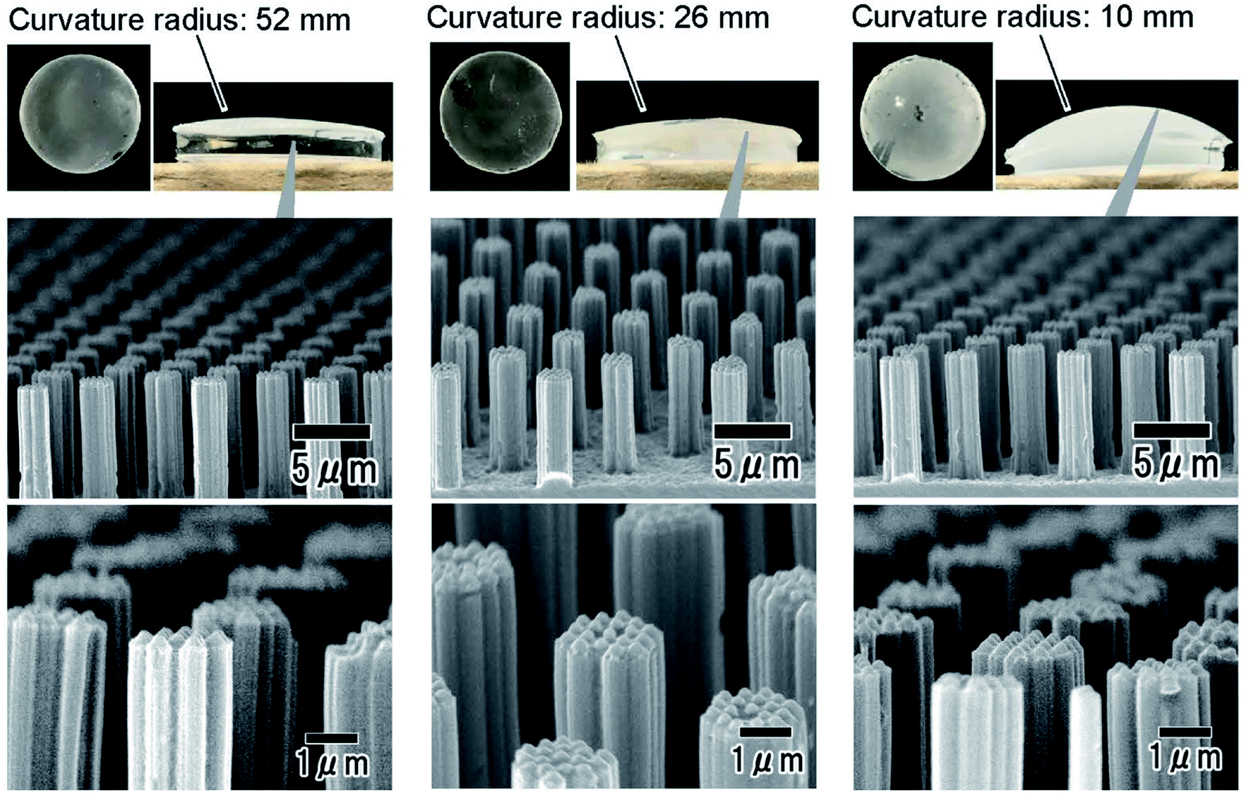 | ||
| Fig. 8 Photographs and SEM images of nanoimprinted specimens with different curvature radii. | ||
Fig. 9(a) shows the observed results of hierarchical pillar arrays obtained by the 1st, 5th, and 10th photo-nanoimprinting using the same flexible mold. In all samples, the formation of a 2 μm-diameter, 4 μm-high micropillar array with a nanopillar array at the tip was confirmed. These results show that flexible molds made of PDMS can be used repeatedly. Fig. 9(b) shows the measured contact angles with water droplets exhibited by the surfaces obtained by the 1st through the 10th nanoimprinting. The wettability of the fine patterns obtained by nanoimprinting was evaluated using patterns formed on a smooth substrate rather than on a curved substrate. All of the samples exhibited a water-drop contact angle of approximately 155° and were confirmed to have high waterrepellency. Although the static contact angle could not be measured because of the difficulty in placing the water droplets on the surface, the curved surfaces with the hierarchical pillar arrays were also observed to exhibit high water repellency.
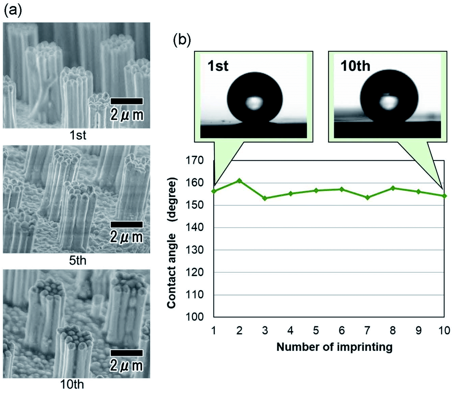 | ||
| Fig. 9 (a) SEM images of hierarchical pillar arrays formed by 1st, 5th, and 10th photo-nanoimprinting using same flexible mold. (b) Contact angles of water droplet on hierarchical pillar arrays. | ||
Conclusions
Flexible molds with hierarchical patterns were fabricated using a hierarchical pillar array prepared by the anodization of Al as a template. Photo-nanoimprinting using the obtained flexible molds enabled the formation of ordered pillar arrays with micro-nano hierarchical structures on the surfaces of tubular substrates and convex lenses. The flexible molds obtained in this study deform following the shape of the substrate, indicating that the flexible molds are effective for preparing fine patterns on surfaces with various curved shapes. The structure of the hierarchical pillars formed on the substrate could also be controlled by changing the geometrical structures of anodic porous alumina used as the starting material. Contact angle measurements of the surfaces with the hierarchical pillar array obtained by this process confirmed superhydrophobic properties with a water-drop contact angle exceeding 150°. In addition, the molds could be used repeatedly, and the water repellency of the surfaces obtained from the 1st to the 10th photo-nanoimprinting remained almost the same. This method is promising for imparting superhydrophobic properties based on micro-nano hierarchical patterns on curved surfaces.Author contributions
T. Yanagishita.: conceptualization, methodology, investigation, writing – original draft. T. Sou: investigation. H. Masuda: writing – review & editing.Conflicts of interest
There are no conflicts to declare.Acknowledgements
The present work was supported by The Fujikura Foundation.References
- J. Chen, H. Nie, C. Tang, Y. Cui, B. Yan, Z. Zhang, Y. Kong, Z. Xu and P. Cai, Appl. Phys. Express, 2019, 12, 052015 CrossRef CAS.
- J. Chen, S. Chen, P. Gu, Z. Yan, C. Tang, Z. Xu, B. Liu and Z. Liu, Carbon, 2020, 162, 187 CrossRef CAS.
- J. Chen, C. Yang, P. Gu, Y. Kuang, C. Tang, S. Chen and Z. Liu, J. Lightwave Technol., 2021, 39, 562 CAS.
- J. Chen, Y. Kuag, P. Gu, S. Feng, Y. Zhu, C. Tang, Y. Guo, Z. Liu and F. Gao, J. Lightwave Technol., 2021, 39, 4525 CAS.
- S. Y. Chou, P. R. Krauss and P. J. Renstrom, Appl. Phys. Lett., 1995, 67, 3114 CrossRef CAS.
- A. Gombert, W. Glaubitt, K. Rose, J. Dreibholz, B. Blasi, A. Heinzel, D. Sporn, W. Doll and V. Wittwer, Thin Solid Films, 1999, 351, 73 CrossRef CAS.
- G. Jung, Z. Li, W. Wu, Y. Chen, D. L. Olynick, S. Wang, W. M. Tong and R. S. Williams, Langmuir, 2005, 21, 1158 CrossRef CAS PubMed.
- C. Sun, A. Gonzalez, N. C. Linn, P. Jiang and B. Jiang, Appl. Phys. Lett., 2008, 92, 051107 CrossRef.
- B. Bae, S. Hong, E. Hong, H. Lee and G. Jung, Jpn. J. Appl. Phys., 2009, 48, 010207 CrossRef.
- T. Kim, H. E. Jeong, K. Y. Suh and H. H. Lee, Adv. Mater., 2009, 21, 2276 CrossRef CAS.
- M. H. Lee, N. Lim, D. J. Ruebusch, A. Jamshidi, R. Kapadia, R. Lee, T. J. Seok, K. Takei, K. Y. Cho, Z. Fan, H. Jang, M. Wu, G. Cho and A. Javey, Nano Lett., 2011, 11, 3425 CrossRef CAS PubMed.
- H. Lan and H. Liu, J. Nanosci. Nanotechnol., 2013, 13, 3145 CrossRef CAS PubMed.
- H. Cho, J. Kim, H. Park, J. W. Bang, M. S. Hyun, Y. Bae, L. Ha, D. Y. Kim, S. M. Kang, T. J. Park, S. Seo, M. Choi and K. Suh, Nat. Commun., 2014, 5, 3137 CrossRef PubMed.
- J. W. Leem, S. K. Soo, H. Lee, J. A. Rogers, E. Kim and J. S. Yu, Adv. Energy Mater., 2014, 4, 1301315 CrossRef.
- D. Linklater, S. Saita, T. Murata, T. Yanagishita, C. Dekiwadia, R. Crawford, H. Masuda, H. Kusaka and E. Ivanova, ACS Appl. Nano Mater., 2022, 5, 2578 CrossRef CAS.
- M. Beck, M. Graczyk, I. Maximow, E.-L. Sarwe, T. I. G. Ling, M. Keil and L. Montelius, Microelectron. Eng., 2002, 61–62, 441 CrossRef CAS.
- T. Yanagishita, T. Endo, K. Nishio and H. Masuda, Jpn. J. Appl. Phys., 2010, 49, 065202 CrossRef.
- T. Yangishita and H. Masuda, Mater. Lett., 2015, 160, 235 CrossRef.
- T. Yanagishita, M. Yoshida and H. Masuda, Langmuir, 2021, 37, 10573 CrossRef CAS PubMed.
- H. Masuda and K. Fukuda, Science, 1995, 268, 1466 CrossRef CAS PubMed.
- T. Yanagishita, T. Hidaka, M. Suzuki and H. Masuda, J. Vac. Sci. Technol., B: Nanotechnol. Microelectron.: Mater., Process., Meas., Phenom., 2016, 34, 021804 Search PubMed.
- T. Yanagishita, M. Omata and H. Masuda, Jpn. J. Appl. Phys., 2022, 61, 038001 CrossRef.
- Z. Lin, Y. Gu, L. Wang, H. Ge, W. Wu, Q. Xia, C. Yuan, Y. Chen, B. Cui and R. S. Williams, Nano Lett., 2009, 9, 2306 CrossRef PubMed.
- B. Farshchian, A. Amirsadeghi, S. M. Hurst, J. Wu and J. Lee, Microelectron. Eng., 2011, 88, 3287 CrossRef CAS.
- J. Chen, C. Gu, H. Lin and S. Chen, Opt. Express, 2015, 23, 20977 CrossRef CAS PubMed.
- T. Yanagishita, T. Murakoshi, T. Kondo and H. Masuda, RSC Adv., 2018, 8, 2041 RSC.
- T. Yanagishita, T. Hayakawa, T. Kondo and H. Masuda, RSC Adv., 2021, 11, 2096 RSC.
- T. Yanagishita, K. Kato, N. Shirano and H. Masuda, ECS J. Solid State Sci. Technol., 2022, 11, 013001 CrossRef.
- A. Marmur, Langmuir, 2003, 19, 8343 CrossRef CAS.
- K. Autumn, Y. A. Liang, S. T. Hsieh, W. Zesch, W. P. Chan, T. W. Kenny, R. Fearing and R. J. Full, Nature, 2000, 405, 681 CrossRef CAS PubMed.
- H. Masuda and M. Satoh, Jpn. J. Appl. Phys., 1996, 35, 126 CrossRef.
| This journal is © The Royal Society of Chemistry 2022 |