
 Open Access Article
 This Open Access Article is licensed under a Creative Commons Attribution-Non Commercial 3.0 Unported Licence
Recycling and applications of ammonium polyphosphate/polycarbonate/acrylonitrile butadiene styrene by laser-scribing technologies for supercapacitor electrode materials
Weiwei Yang *,
Chao Yu and
Fanxing Meng
*,
Chao Yu and
Fanxing Meng
Norinco Group Air Ammunition Research Institute Co., Ltd, Harbin 100000, China. E-mail: yangweiwei0811@163.com
First published on 29th June 2022
Abstract
Fabricating a simple and valid high-property graphene-based supercapacitor employing engineered plastic waste as the original material has attracted tremendous interest. Herein we report an extendable method for producing nitrogen and phosphorus dual-doped porous three-dimensional (3D) graphene materials from the blends of ammonium polyphosphate (APP) and polycarbonate (PC)/acrylonitrile ((A), butadiene (B), and styrene (S)) (ABS) using a simple laser direct-writing technique. In APP/PC/ABS blends, APP/PC/ABS, a waste by-product generated in car interiors and exterior decoration and electronic device shells and other fields, served as a sufficient and economic carbon source, while APP was employed as a nitrogen and phosphorus source as well as flame retardant. APP/PC/ABS blends could be transformed into nitrogen and phosphorus dual-doped laser-induced graphene (NPLIG) via scribing under a CO2 laser in air conditions. In addition, a supercapacitor was fabricated applying NPLIG as the electrode material, and KOH solution as the electrolyte. The as-fabricated NPLIG supercapacitor exhibited excellent electrochemical behaviours, namely, a high specific areal capacitance (239 F g−1) at a current density of 0.05 A g−1, which outperformed many LIG-based and GO-based supercapacitors. The concept of designing supercapacitors that can be obtained with a facile laser-scribing technology can stimulate both the building of supercapacitors and preparation of graphene, and the sustainable utilization of engineering plastics.
1 Introduction
With the fast development of personal portable facilities, smart electronic equipment has been widely applied in people' daily lives, resulting in an urgent demand for energy-storage systems with high power density, excellent cycling durability, and a fast charging and discharging speed. In this aspect, supercapacitors, which possess the advantages of long longevity, high power density, and low inside resistance,1 have been widely applied in energy-storage equipment. Therefore, much effort has been dedicated to fabricating high-performance and low-cost supercapacitors.2 Among numerous reported capacitor devices, electric double-layer capacitors (EDLCs), as a perfect energy carrier, are a kind of widely investigated capacitor, in which energy is stored through ion attachment between the electrode and electrolyte interface.3 Hence, the performance of EDLCs is determined by the surface area of the electrode. This reliance has promoted porous carbon-based electrode materials to be recognized as prospective candidates for energy-storage utilization due to their large surface area, superior conductivity, and reasonable cost.4As a popular carbon material, three-dimensional (3D) graphene has displayed great potential for the fabrication of high-capacity energy-storage devices.5–10 To date, numerous methods have been promoted for the generation of graphene, for instance, the mechanical exfoliation of graphite, redox method, and laser-induced technology. Among these methods, laser-induced technique possesses the merits of facile use, low-cost, and environmental friendliness, among other merits.11,12 These advantages make laser-induced technology a better choice for the low-priced generation of graphene-based supercapacitors with high electrochemical performance.13,14 For instance, Tour et al. fabricated porous graphene by scanning on a polyimide (PI) matrix through CO2 laser induction and the prepared laser-induced graphene (LIG) displayed excellent applications in energy-storage fields. In addition, previous studies have indicated that adding nitrogen (N) and phosphorus (P) and other heteroatoms to graphene is a valid approach to enhance the capacitive behaviour of LIG because of the increased electrochemical active sites.15,16 In recent years, the preparation of multi-hybrid atom-doped graphene has also emerged as an approach to improve the storage performance of supercapacitors. Furthermore, both experimental and theoretical investigations have illustrated that NP dual-doped graphene displays increased electrochemical properties.17,18 Despite the increased electrochemical performance, the preparation processes of N and P dual-doped graphene frequently require either elevated temperature or multistep chemical reactions, restricting its widespread applications. Therefore, it is critical to develop a simple and effective method for the preparing of NP dual-doped graphene.
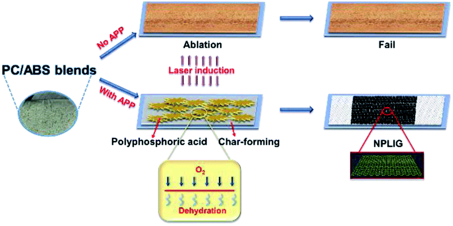
Motived by the robust laser-induced technology, we aimed to prepare NP-doped graphene via straightforward laser scribing on a polymer substrate with abundant N and P elements. According to the research conclusions of Tour's team, the structural features of a substrate capable of preparing LIG generally require it to have aromatic and imide repeat units.19 Recently, the most widely studied materials that can be used as hybrid atom-doped LIG substrates are engineering plastics with high thermal stability, such as polyimide, PES, and other engineering materials. These materials are relatively expensive and/or require complicated processing technology. Therefore, there is a critical need to find a low-cost material that can be used to prepare NP-doped LIG (NPLIG). We supposed that LIG may be directly fabricated via laser scribing on PC/ABS due to its aromatic structure. Recently, adding ammonium polyphosphate (APP) into PC/ABS has been utilized as a common approach to broaden its application fields; thus, it is now a main waste by-product generated in the electronic and electrical industry that has commercial value but was once considered useless and environmentally unfriendly. However, Tour was convinced that PC/ABS cannot be directly converted to LIG. As previous research reported, the substrate materials have an extremely high flame retardancy;19 thus, we aimed to use APP/PC/ABS as the matrix to prepare LIG materials. Here, the PC/ABS was able to support the C content, and APP may support N and P content. Moreover, the transformation of APP/PC/ABS into practical products is of great importance to the sustainable evolution of society, whether it is from a business or scientific aspect.20,21
In this work, we propose a facile approach for preparing NPLIG by laser direct scribing on APP/PC/ABS composites. The formation of graphene in APP/PC/ABS can be ascribed to the aromatic structure of the PC/ABS matrix and the photothermal effect provided by the simple laser radiation. The resulting NPLIG could be prepared in ambient conditions in an optimized experimental process comprising multiple laser-scribing process steps (10% total laser power: 5 W, laser-scribing rate: 10 mm s−1). The NPLIG displayed high electrical conductivity (5 Ω, 1 × 1 cm2), which is a characteristic required for application in the area of electronics. The potential for utilization of the NPLIG composite was illustrated in N and P dual-doped supercapacitor electrodes and was shown to be based on the high conductivity of NPLIG. The concept of designing NPLIG supercapacitors fabricated with a facile laser-induced technology can be attractive for both building supercapacitors and the preparation of graphene and for the sustainable utilization of APP/PC/ABS and other engineering plastics.
2 Materials and methods
2.1 Preparation of APP/PC/ABS splines
PC/ABS and APP pellets were dried at 80 °C in a vacuum for 8 h. Then, PC/ABS, and APP were mixed in an injection moulding machine at 215° for 10 min. The mixtures were pressed into sheets for different characterizations. The compositions of the APP/PC/ABS composites are listed in Table 1. As shown in Table 1, four samples with different proportions were made, comprising PC/ABS material without APP; 5% APP/PC/ABS with 5 wt% APP and 95 wt% PC/ABS; 10% APP/PC/ABS with 10 wt% APP and 90 wt% PC/ABS; and 15% APP APP/PC/ABS with 15 wt% APP and 85 wt% PC/ABS.| Samples | PC/ABS(wt%) | APP(wt%) |
|---|---|---|
| 1 | 100 | 0 |
| 2 | 95 | 5 |
| 3 | 90 | 10 |
| 4 | 85 | 15 |
2.2 Preparation of NPLIG
APP/PC/ABS splines were scribed directly using a CO2 laser (10.6 μm) instrument (Ketai 4060 purchased from Shandong Kaitai Laser Equipment Co., Ltd, Liaocheng, China). The full laser power was 50 W and the applied laser power was 5 W. The scan speed and laser DPI were 10 mm s−1 and 1000 (dots per inch), respectively. In the scribing progress, the focus mode was adopted for reducing the dispersion of the laser energy. The prepared NPLIG was marked according to the laser passes. For instance, NPLIG scribed at a laser pass of one pass was denoted as LIG-1×. All the experiments were carried out at room temperature and atmospheric conditions.2.3 Fabrication of NPLIG supercapacitor
For more accurate performance testing, the NPLIG was scraped from the APP/PC/ABS matrix. The NPLIG powders and conductive carbon black and PTFE (poly tetra fluoroethylene) were mixed in a ratio of 8![[thin space (1/6-em)]](https://www.rsc.org/images/entities/char_2009.gif) :1:1 and ground uniformly. The conductive paste was ultrasonically dispersed for 30 min in sonicated deionized water. The conductive paste was dropped onto clean foamed nickel with a pipette gun, and then placed in an oven for drying for 12 h. An electrode sample was obtained, and a mass of ≈1–2 mg was selected for the electrochemical measurements.
:1:1 and ground uniformly. The conductive paste was ultrasonically dispersed for 30 min in sonicated deionized water. The conductive paste was dropped onto clean foamed nickel with a pipette gun, and then placed in an oven for drying for 12 h. An electrode sample was obtained, and a mass of ≈1–2 mg was selected for the electrochemical measurements.
2.4 Material characterization
The surface morphology of all the samples was observed by scanning electron microscopy (SEM: JSM-IT300) and transmission electron microscopy (TEM: FEI Tecnai G2 F30). To further analyze the layers of NPLIG, the NPLIG was characterized by atomic force microscopy (AFM), (Bruker Dimension Icon). Raman spectra were obtained on a Micro Raman imaging spectrometer (DXRxi) with a wavelength of ≈532 nm. X-ray diffraction (XRD) (D8 advance) and X-ray photoelectron spectroscopy (XPS) (Thermo Kalpha) spectra were performed. Thermogravimetric analysis (TGA) thermograms were recorded (Q50 TGA Instruments) at a rate of 10 °C min−1 under an argon atmosphere, and temperature range from 100 °C to 900 °C. The conductivity of NPLIG was measured with a standard resistance tester (YD 2511A). NPLIG samples were scratched off from the APP/PC/ABS matrix for further characterization by XRD, XPS, and thermogravimetric analysis. Other general characterizations were carried out directly on the NPLIG surface.According to the Raman spectroscopy data, the crystalline size could be determined by the following eqn (1):22
 | (1) |
 is the ratio of the intensities of the G peak and D peak.
The limiting oxygen index (LOI) of LIG/APP/PC/ABS as a flame-retardant coating was tested on a JF-3 Oxygen Index system purchased from Nanjing Jiangning Analytical Instrument Co., Ltd (Nanjing, China) in accordance with the ASTM D2863-2008 standard. The spline size investigated was 130 × 6.5 × 3 mm3. A UL-94 vertical burning tester was used on the CZF-5 according to the ANSI/UL-94-2010 standard. The spline size was 130 × 13 × 3 mm3.
2.5 Electrochemical measurements
The electrochemical performance of the NPLIG supercapacitor working electrode (for the detailed preparation method, see Section 2.3) was carried out using cyclic voltammetry (CV) with a three-electrode configuration, galvanostatic charge–discharge (GCD), and electrochemical impedance spectroscopy (EIS), which were measured on a CHI 660 workstation. EIS of the NPLIG supercapacitor devices was performed at an open circuit voltage in the frequency range from 0.01 Hz to 100 KHz.The specific capacitance of the material by weight (Cs) were calculated from the GCD curves according to eqn (2).23
 | (2) |
3 Results and discussion
3.1 Morphology and structural characterization
The previously studied matrix materials for preparing LIG have high thermal stability and good flame-retardant performance (UL-94 level can reach the V-0 level), such as polyimide,19–21 such that the high temperature generated by the laser scribing always affords LIG rather than leading to ablation or melt damage of the matrix materials. The flame-retardant performances of APP/PC/ABS with different amounts of APP are shown in Fig. 1, and it can be seen that when the APP addition amount was 15%, the flame-retardant grade reached the highest level.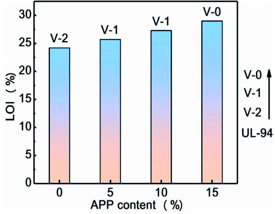 | ||
| Fig. 1 LOI values and UL-94 levels of APP/PC/ABS with different APP contents. | ||
In order to further determine the addition amount of APP, we conducted laser induction on samples with different APP contents (0–15%), and the prepared samples were subjected to Raman testing (Fig. 2). Further convinced that the degree of graphitization is the best when the APP addition is 15%, the material selected for the matrix materials characterization was APP/PC/ABS material with 15% APP added, which was denoted as APP/PC/ABS.
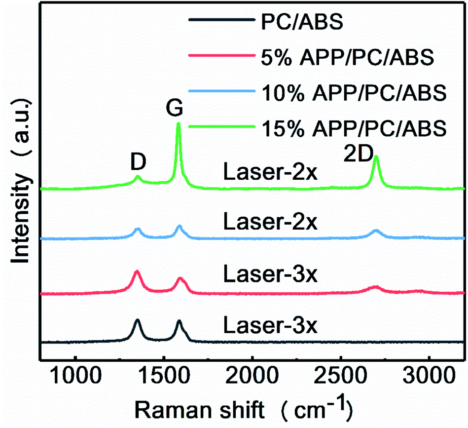 | ||
| Fig. 2 Raman spectra of the laser-induced products of the APP/PC/ABS composite substrates with different APP contents. | ||
The fabrication process of NPLIG and the supercapacitor device are schematically illustrated in Fig. 1. In order to directly generate the NPLIG, PC/ABS containing APP as a precursor was placed on the laser scanning platform (The detail description is shown in Fig. 3a). The APP/PC/ABS splines were scribed under 10.6 μm with a CO2 laser, in which the laser generated an extremely high local temperature (>2500 °C)24, while the precursor underwent graphitization,25 leading to the formation of an NPLIG rectangular electrode material. The NPLIG on APP/PC/ABS could be obtained in several minutes. The fabrication of NPLIG with various geometries could be tuned via controlling the computer connected to the laser. As Fig. 1b shows, the NPLIG electrode was fabricated by preparing it in conductive paste. Subsequently, for the L-P LIG electrodes, a Hg/HgO electrode (reference electrode) and Pt electrode (counter electrode) were used to assemble a supercapacitor device (Fig. 3b).
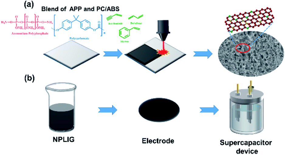 | ||
| Fig. 3 Schematic illustration of the fabrication processes of the NPLIG supercapacitor. (a) Preparation of NPLIG. (b) Fabrication processes of the NPLIG supercapacitor. | ||
The morphology and structure of NPLIG were investigated by SEM and TEM. It is worth noting that the surface morphology of the NPLIG derived from APP/PC/ABS was distinctly different from that of the APP/PC/ABS matrix. In other words, the morphology of NPLIG was a sheet structure; however, the morphology of the APP/PC/ABS matrix remained unchanged. As shown in the inset in Fig. 4a, the laser path appeared regularly by laser scanning, and there were a large number of pores, which made the surface rough (Fig. 4b, c). The pores were generated by the gaseous products (for instance CO2, H2O, and NxOy26) formed during the CO2 laser-scribing process, which caused the (incomplete) decomposition of APP/PC/ABS. In addition, these pores ranged from micropores to macropores. The macropores could be readily observed in the TEM image (Fig. 4d), with the above results also in the SEM and TEM images. Wrinkled structures and few layers (less than 10 layers) could be observed in some regions from the TEM images (Fig. 4e), which were generated by overlapping graphene sheets or crimping at the edge.27–29 The high-resolution TEM image (Fig. 4f) revealed the existence of NPLIG, because the image displayed a feature with a 0.34 nm d-spacing of graphene. Besides, the lattice space of 0.34 nm corresponded to the (002) planes in graphic carbon,30 which illustrated the presence of rolled or folded graphene in the NPLIG, corresponding to the wrinkled structure shown in the TEM images. The above results concluded that APP/PC/ABS was successfully converted into 3D hierarchical porous graphene via laser scribing. EDX mappings (Fig. 4g–k) displayed a uniform distribution of C, O, N, and P elements on the surfaces of NPLIG, further suggesting the successful doping of nitrogen and phosphorus elements.31
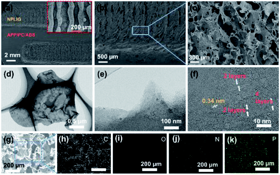 | ||
| Fig. 4 Morphology and structure of NPLIG. (a) SEM image of a cross-section of the NPLIG sample; (b) enlarged SEM cross-section image of the NPLIG area. The smooth region is the APP/PC/ABS substrate. The porous region is the NPLIG layer; (c) high-resolution SEM image of the NPLIG formed on APP/PC/ABS; (d–f) high-resolution TEM images of NPLIG; (g–k) EDS images of NPLIG. C (h), O(i), P (j), N (k). | ||
Fig. 5 displays the BET curves of NPLIG. The BET curves (Fig. 5) revealed once again the NPLIG electrode materials comprised an ordered and porous structure consisting of micropores, mesopores, and macropores. Normally, the micropores can enhance the active surface area of supercapacitor electrode materials, while the macropores are beneficial for the ion-transport, which should favour an increase in the electrochemical performance.
 | ||
| Fig. 5 BET curves of NPLIG. | ||
To further analyze the layers of N,P LIG, the N,P LIG was characterized by atomic force microscopy (AFM). Fig. 6 a presents the AFM image of NPLIG, and Fig. 6b–d are the AFM surface height plots corresponding to the positions marked 1, 2, and 3 in Fig. 6 a, respectively. It can be seen from Fig. 6a that NPLIG was a sheet with an uneven size. Combined with Fig. 6b–d, it could be seen that the sheet height of graphene was 3.8–4.8 nm. Since the thickness of single-layer graphene was about 0.7 nm32,33, the number of layers of the prepared NPLIG was less than 10 and the number of sheets was uniform. At location 1, the Ra was 2.276 nm and the surface distance was 0.591 μm; at location 2, the Ra was 1.129 nm and the surface distance was 0.583 μm; at location 3, the Ra was 0.710 nm and the surface distance was 0.596 μm. These results were consistent with the results from the TEM analysis.
 | ||
| Fig. 6 (a)AFM image and (b–d) surface height plots for NPLIG corresponding to the positions marked 1, 2, and 3 in (a). | ||
The graphite structure of NPLIG was also determined by X-ray diffraction (XRD). Fig. 7a shows the XRD patterns of NPLIG (laser scribing with four laser passes). Peaks at approximately 25.9°and 42.9°appeared in NPLIG after scribing on APP/PC/ABS, which could be ascribed to the (002)34 and (100) planes of graphene.35,36 The peak at 25.9° (2θ) illustrated an interlayer spacing of 0.34 nm, indicating a high level of graphitization. This result matched with the above-mentioned TEM results.
 | ||
| Fig. 7 Physicochemical properties of NPLIG. (a) XRD pattern of NPLIG; (b) Raman spectra of NPLIG and the APP/PC/ABS matrix; (c) XPS survey spectra of NPLIG and the APP/PC/ABS matrix; (d) high-resolution images of C 1s; (e) high-resolution images of N 1s; (f) high-resolution images of P 2p spectra; (g) Raman spectra curve of NPLIG prepared with different laser-scribing passes (laser 1× to laser 5×); (h) peak ratio of the G peak and D peak of NPLIG prepared with different laser-scribing passes; (i) resistance of NPLIG prepared with different laser-scribing passes. | ||
Fig. 7b shows the Raman spectra of NPLIG (laser scribed with four laser passes) and the APP/PC/ABS matrix. Comparing pristine APP/PC/ABS to NPLIG, the curves were obviously different. There were three prominent peaks in the Raman spectra of NPLIG. The G peak was located at 1580 cm−1, which corresponded to sp2-type ordered graphitic carbon. The D peak was near 1350 cm−1, which was considered to be the sp3-type disordered carbon peak of LIG. The G peak reflected the number of layers of NPLIG. The 2D peak was due to the double-phonon resonance Raman peak at 2700 cm−1, which corresponded to the second-order zone-boundary phonons.37,38
The XPS survey spectrum gave information on the chemical composition of the samples of NPLIG and the APP/PC/ABS matrix, revealing the presence of C, O, N, and P (Fig. 7c) in NPLIG, which was consistent with the EDX mapping. The high-resolution C 1s spectrum in Fig. 7d could be deconvoluted into four prominent peaks for C–C (sp2 hybridized graphitic carbon, ∼284.6 eV), C–O (carbon in carbon oxide bonds, ∼285.5 eV), O![[double bond, length as m-dash]](https://www.rsc.org/images/entities/char_e001.gif) C–N (≈286.7 eV), and O–CO (≈289.0 eV).39 The existence of sp2 hybridized graphitic carbon, and nitrogen-containing and oxygen-containing groups indicated the successful conversion of APP/PC/ABS into the graphite form of carbon. The high-resolution XPS spectrum of N 1s exhibited four notable peaks with binding energies at 398.5 eV (pyridinic N), 399.9 eV (pyrrolic N), 401.2 eV (graphitic N), and 403.8 eV (oxidized N), which were attributed to N–6, N–5, N–Q, and N–O. Pyrrolic N could be applied as a functional and active site to promote the diffusion of reactive metal ions (such as Na+ and Li+), hence further enhancing the electrochemical performance of the hybrid. Graphitic N benefits increasing the electrical conductivity of the NPLIG due to the mutation of the electron-donor characteristics in graphitic carbon and the binding to three sp2-carbon atoms.40,41 This indicates that the presence of nitrogen moieties is in favour of electron transfer and the diffusion kinetics of electrolyte ions.42 The high-resolution XPS spectrum of P 2p exhibited two notable peaks at 130.1 and 132.0 eV, corresponding to the P–C and P–O bonds, respectively.43 The existence of phosphorus is beneficial for open edge sites and the formation of a wrinkle morphology, and which can improve the electrochemical performance of NPLIG electrode materials. Accordingly, the prepared NPLIG material was successfully doped with both N and P atoms.
C–N (≈286.7 eV), and O–CO (≈289.0 eV).39 The existence of sp2 hybridized graphitic carbon, and nitrogen-containing and oxygen-containing groups indicated the successful conversion of APP/PC/ABS into the graphite form of carbon. The high-resolution XPS spectrum of N 1s exhibited four notable peaks with binding energies at 398.5 eV (pyridinic N), 399.9 eV (pyrrolic N), 401.2 eV (graphitic N), and 403.8 eV (oxidized N), which were attributed to N–6, N–5, N–Q, and N–O. Pyrrolic N could be applied as a functional and active site to promote the diffusion of reactive metal ions (such as Na+ and Li+), hence further enhancing the electrochemical performance of the hybrid. Graphitic N benefits increasing the electrical conductivity of the NPLIG due to the mutation of the electron-donor characteristics in graphitic carbon and the binding to three sp2-carbon atoms.40,41 This indicates that the presence of nitrogen moieties is in favour of electron transfer and the diffusion kinetics of electrolyte ions.42 The high-resolution XPS spectrum of P 2p exhibited two notable peaks at 130.1 and 132.0 eV, corresponding to the P–C and P–O bonds, respectively.43 The existence of phosphorus is beneficial for open edge sites and the formation of a wrinkle morphology, and which can improve the electrochemical performance of NPLIG electrode materials. Accordingly, the prepared NPLIG material was successfully doped with both N and P atoms.
3.2 Influence of the laser process parameters on NPLIG formed on the APP/PC/ABS composite
The influence of different laser passes on generating NPLIG was investigated by adjusting the laser-scribing parameters. One set of NPLIG samples was prepared by applying one to five laser-scribing passes (LIG 1× to LIG 5×) with a laser power of 10% of the total power (5 W) and a scribing rate of 10 mm s−1 (Fig. 7g). When APP/PC/ABS was irradiated under one laser pass, a wide D peak and very faint 2D peak were noted, revealing that low-graphitic carbon was obtained. As the laser pass increased from one pass to five passes, the intensity of the D peak declined, whereas the intensities of the G peak and 2D peak were enhanced, denoting the gradual generation of higher quality graphitic structure. The largest IG/ID ratio (7.5, Fig. 7h) of LIG 4× indicated the crystallite size of LIG 4× was the largest (La = 144.2 nm). The LIG 4× had the smallest IG/I2D ratio, which demonstrated the fewest quantity of LIG 4× layers. Moreover, the resistance of NPLIG (LIG 1× to LIG 5×) was measured, as seen in Fig. 7i, illustrating the smallest resistance of LIG 4× (the resistance test device is shown in the inset in Fig. 7i). These results suggest that a suitable laser pass usually results in the acquisition of superior quality graphene.443.3 Growth mechanism of NPLIG formed on APP/PC/ABS
The mechanism of APP/PC/ABS transforming into NPLIG under ambient air conditions is illustrated in Fig. 8. A photothermal influence may be generated via direct laser scribing, which results in a large local temperature, combustion corrosion, and depolymerization of the APP/PC/ABS composite. Attributed to the barrier effect of APP,45 APP degradation generated phosphoric acid and metaphosphoric acid, which could catalyse the PC/ABS into amorphous carbon. Therefore, the surface of APP/PC/ABS was transformed into amorphous carbon first;46 whereas continuous exposure to the laser scribing promoted the transformation of the amorphous carbon into a graphitized structure. The high temperature generated by the laser scribing broke the CO and N–C bonds,47–49 which was verified by the elemental decrease of oxygen and nitrogen according to the XPS analyses. The remaining N, P, and C atoms recombined and “recrystallized” into NPLIG.
 | ||
| Fig. 8 Growth mechanism of NPLIG formed on APP/PC/ABS. | ||
3.4 Electrochemical performance
The electrochemical performance of an as-fabricated supercapacitor with KOH as the electrolyte was investigated employing cyclic voltammetry (CV) and galvanostatic charge–discharge tests in a potential window from 0 to 0.8 V. NPLIG served as the active electrode. Fig. 9a and b displays the CV curves of the supercapacitor fabricated with NPLIG electrodes via laser scribing over four passes. All the CV curves (scan rate range from 100 mV s−1 to 10 V s−1) were symmetric pseudo-rectangular, which suggested the charge storage involved a double-layer capacitor mechanism. When the scanning rate was 1 V s−1, no pseudocapacitive performance was shown and no anodic and cathodic peaks are displayed in Fig. 9a and b. Even when the scan rate was increased to 10 V s−1, NPLIG keeping the quasi-rectangular CV curves at various scan rates demonstrated its superior EDLC behaviour. The above results evidence that NPLIG is a potential supercapacitor electrode material. This superior capacitive behaviour was confirmed by the GCD measurement at various current densities ranging from 0.05 to 1 A g−1 (Fig. 9c). | ||
| Fig. 9 Electrochemical performances of the supercapacitor fabricated using NPLIG electrodes. (a and b) CV curves of the NPLIG electrode at a scan rate ranging from 0.1 to 10 V s; (c) GCD curves of the NPLIG electrode at various current densities ranging from 0.05 to 1 A g−1; (d) the specific capacitance (Csc) of NPLIG in the current density range from 0.05 to 1 A g−1. | ||
As illustrated in Fig. 9d, the specific areal capacitance calculated from the GCD curves for NPLIG was consistent with the conclusion acquired from the CV curves. NPLIG could deliver a specific areal capacitance of 239 F g−1 at the current density of 0.05 A g−1. This specific areal capacitance was superior to that for the LIG without hybrid atoms doping reported in previous studies at the same current density,50 and it was also superior to the values obtained in previous research on GO-derived supercapacitors.51–54 The high specific capacitance value of the NPLIG supercapacitor encountered here may be attributed to the hierarchical porous structure, which resulted in the high capacitance.55 This structural characteristic has a high specific surface area with plentiful wrinkles and supports facile access for the generation of Helmholtz layers between the electrolyte and the NPLIG electrode. It is expected that these findings verify this innovative method here and may stimulate scholars to further study the mechanisms and explore the potential of other polymers.
In order to explain the electrochemical reaction kinetics of the NPLIG electrode, the electrochemical impedance of the NPLIG electrode was measured and analyzed. Fig. 10 illustrates the AC impedance spectrum of NPLIG electrode material (current density was 1 A g−1), where the impedance curve displays an obvious semicircle in the high-frequency region and a straight line in the low-frequency region. The semicircular arc in the high-frequency region represents the surface charge-transfer resistance (Rct) of the electrode material, and the oblique line in the low-frequency region represents the Warburg resistance caused by concentration polarization. Fig. 10 shows that the Rct value of LIG-APP/PC/ABS was small, only 20 Ω, which indicated that the electrode material had a small internal resistance.56 Combined with the above results, NPLIG has an excellent capacitance.
 | ||
| Fig. 10 Nyquist plots of the NPLIG electrode. | ||
4 Conclusions
In summary, for the first time, APPPC/ABS blends were scribed directly by applying a CO2 laser (10.6 μm) at different laser passes to successfully prepare N and P dual-doped laser-induced graphene (LIG) with a 3D porous structure. Electrochemical performance tests of an as-fabricated NPLIG supercapacitor were carried out using a three-electrode test method, and using KOH as the electrolyte. The as-prepared NPLIG exhibit excellent electrochemical behaviour with a high specific area capacitance of 239 F g−1 at a current density of 0.05 A g−1, which outperformed a large number of the reported LIG-based supercapacitors. The method of preparing graphene via scribing using a CO2 laser is an environmentally friendly and sustainable process, which does not generate toxic or harmful waste. The usage of APP/PC/ABS with high flame retardancy and environmental friendliness facilitates its wider applications, helping turn APP/PC/ABS from garbage into a commercial commodity and affording additional precursors for preparing graphene.Conflicts of interest
There are no conflicts to declare.Acknowledgements
Dr Weiwei Yang and the co-authors would like to thank all the reviewers who participated in the review of this manuscript.Notes and references
- A. K. Shukla, A. Banerjee, M. K. Ravikumar and A. Jalajakshi, Electrochim. Acta, 2012, 84, 165–173 CrossRef.
- M. Vangari, T. Pryor and L. Jiang, J. Energy Eng., 2013, 139, 72–79 CrossRef.
- T. Chen, M. Li, S. Song, P. Kim and J. Bae, Nano Energy, 2020, 71, 104549 CrossRef CAS.
- F. Wang, X. Wu, X. Yuan, Z. Liu, Y. Zhang, L. Fu, Y. Zhu, Q. Zhou, Y. Wu and W. Huang, Chem. Soc. Rev., 2017, 46, 6816–6854 RSC.
- V. C. T. Matthew, J. Allen and R. B. Kaner, Chem. Rev., 2010, 110, 132–145 CrossRef PubMed.
- D. Bitounis, H. Ali-Boucetta, B. H. Hong, D. H. Min and K. Kostarelos, Adv. Mater., 2013, 25, 2258–2268 CrossRef CAS PubMed.
- G. C. Bong, P. Hoseok, J. P. Tae, S. H. Nam, Y. L. Sang, H. Y. Min, K. Jing and H. H. Won, ACS Nano, 2010, 4, 2910–2918 CrossRef PubMed.
- Y. Sun, Q. Wu and G. Shi, Energy Environ. Sci., 2011, 4, 1113–1132 RSC.
- M. F. El-Kady, V. Strong, S. Dubin and R. B. Kaner, Science, 2012, 335, 1326–1330 CrossRef CAS PubMed.
- Y. Zhai, Y. Dou, D. Zhao, P. F. Fulvio, R. T. Mayes and S. Dai, Adv. Mater., 2011, 23, 4828–4850 CrossRef CAS PubMed.
- L. Li, J. Zhang, Z. Peng, Y. Li, C. Gao, Y. Ji, R. Ye, N. D. Kim, Q. Zhong, Y. Yang, H. Fei, G. Ruan and J. M. Tour, Adv. Mater., 2016, 28, 838–845 CrossRef CAS PubMed.
- D. J. Liaw, K. L. Wang, Y. C. Huang, K. R. Lee, J. Y. Lai and C. S. Ha, Prog. Polym. Sci., 2012, 37, 907–974 CrossRef CAS.
- Y. Li, D. X. Luong, J. Zhang, Y. R. Tarkunde, C. Kittrell, F. Sargunaraj, Y. Ji, C. J. Arnusch and J. M. Tour, Adv. Mater., 2017, 29, 1700496 CrossRef PubMed.
- G. Xu, Z. A. Jarjes, V. Desprez, P. A. Kilmartin and J. Travas-Sejdic, Biosens. Bioelectron., 2018, 107, 184–191 CrossRef CAS PubMed.
- C. Zhou, K. Zhang, M. Hong, Y. Yang, N. T. Hu, Y. J. Su, L. Y. Zhang and Y. F. Zhang, Chem. Eng. J., 2019, 385, 123720 CrossRef.
- F. Zhang, E. Alhajji, Y. J. Lei, N. Kurra and N. H. Alshareef, Adv. Energy Mater., 2018, 8, 1800353 CrossRef.
- H. Wu, X. Li, J. Ren, Q. J. Zheng, C. G. Xu and D. M. Lin, J. Mater. Chem. A, 2017, 5, 20458–20472 RSC.
- C. Han and Z. Chen, Energy, 2021, 214, 118808 CrossRef CAS.
- J. Lin, Z. Peng, Y. Liu, F. Ruiz-Zepeda, R. Ye, E. L. Samuel, M. J. Yacaman, B. I. Yakobson and J. M. Tour, Nat. Commun., 2014, 5, 5714 CrossRef CAS PubMed.
- A. J. Ragauskas, G. T. Beckham, M. J. Biddy, R. Chandra, F. Chen, M. F. Davis, B. H. Davison, R. A. Dixon, P. Gilna, M. Keller, P. Langan, A. K. Naskar, J. N. Saddler, T. J. Tschaplinski, G. A. Tuskan and C. E. Wyman, Science, 2014, 344, 1246843 CrossRef PubMed.
- M. P. Pandey and C. S. Kim, Chem. Eng. Technol., 2011, 34, 29–41 CrossRef CAS.
- L. G. Cançado, K. Takai, T. Enoki, M. Endo, Y. A. Kim, H. Mizusaki, A. Jorio, L. N. Coelho, R. Magalhaes-Paniago and M. A. Pi-menta, Appl. Phys. Lett., 2006, 88, 163106 CrossRef.
- W. W. Yang, Y. Liu, Q. S. Li, J. Wei, X. L. Li, Y. Zhang and J. P. Liu, RSC Adv., 2020, 10, 23953–23958 RSC.
- J. Zhang, M. Ren, Y. Li and J. M. Tour, ACS Energy Lett., 2018, 3, 677–683 CrossRef CAS.
- S. P. Singh, Y. Li, A. Beer, Y. Oren, J. M. Tour and C. J. Arnusch, ACS Appl. Mater. Interfaces, 2017, 9, 18238–18247 CrossRef CAS PubMed.
- H. Wang, H. Wang, Y. Wang, X. Su, C. Wang, M. Zhang, M. Jian, K. Xia, X. Liang and H. Lu, ACS Nano, 2020, 14, 3219–3226 CrossRef CAS PubMed.
- Z. F. Wan, X. Chen and M. Gu, Opto-Electron. Adv., 2021, 4, 200079 CAS.
- F. S. Wen, C. X. Hao, J. Y. Xiang, L. M. Wang, H. Hou, Z. B. Su, W. T. Hu and Z. Y. Liu, Carbon, 2014, 75, 236–243 CrossRef CAS.
- N. Loganathan, K. Munusamy, V. Perumal and B. Pandian, J. Water Environ. Nanotechnol., 2021, 6, 356–366 CAS.
- W. W. Yang, W. Zhao, Q. S. Li, H. Li, Y. L. Wang, Y. X. Li and G. Wang, ACS Appl. Mater. Interfaces, 2019, 12, 3928–3935 CrossRef PubMed.
- W. W. Yang, Y. Liu, J. Wei, X. L. Li, N. H. Li and J. P. Liu, Polymers, 2021, 13, 13060984 Search PubMed.
- N. Mohanty, A. Nagaraja and J. Armesto, Small, 2010, 6, 226–231 CrossRef CAS PubMed.
- B. J. Lee, H. Y. Yu and G. H. Jeong, Nanoscale Res. Lett., 2010, 5, 1768–1773 CrossRef CAS PubMed.
- Z. Wang, J. Cheng, Q. Guan, H. Huang, Y. Li, J. Zhou, W. Ni, B. Wang, S. He and H. Peng, Nano Energy, 2018, 45, 210–219 CrossRef CAS.
- P. Li, Z. Jin, L. Peng, F. Zhao, D. Xiao, Y. Jin and G. Yu, Adv. Mater., 2018, 30, 1800124 CrossRef PubMed.
- X. Ding, Y. Zhao, C. Hu, Y. Hu, Z. Dong, N. Chen, Z. Zhang and L. Qu, J. Mater. Chem. A, 2014, 2, 12355–12360 RSC.
- A. C. Ferrari and D. M. Basko, Nat. Nanotechnol., 2013, 8, 235–246 CrossRef CAS PubMed.
- A. C. Ferrari, J. C. Meyer, V. Scardaci, C. Casiraghi, F. Mauri, S. Piscanec, D. Jiang, K. S. Novoselov, S. Roth and A. K. Geim, Phys. Rev. Lett., 2006, 97, 187401 CrossRef CAS PubMed.
- L. Sheng, H. Jiang, S. Liu, M. Chen, T. Wei and Z. Fan, J. Power Sources, 2018, 397, 325–333 CrossRef CAS.
- Y. Chu, L. Guo, B. Xi, Z. Feng, F. Wu, Y. Lin, J. Liu, D. Sun, J. Feng, Y. Qian and S. Xiong, Adv. Mater., 2018, 30, 1704244 CrossRef PubMed.
- Y. C. Xiao, C. Y. Xu, X. Y. Sun, Y. Pei, P. P. Wang, F. X. Ma and L. Zhen, Chem. Eng. J., 2018, 336, 427–435 CrossRef CAS.
- F. Zhang, E. Alhajji, Y. Lei, N. Kurra and H. N. Alshareef, Adv. Energy Mater., 2018, 8, 1800353 CrossRef.
- C. Zhang, N. Mahmood, H. Yin, F. Liu and Y. Hou, Adv. Mater., 2013, 25, 4932–4937 CrossRef CAS PubMed.
- Y. Chyan, R. Ye, Y. Li, S. P. Singh, C. J. Arnusch and J. M. Tour, ACS Nano, 2018, 12, 2176–2183 CrossRef CAS PubMed.
- J. W. Gu, G. C. Zhang, S. L. Dong, Q. Y. Zhang and J. Kong, Surf. Coat. Technol., 2007, 201, 7835–7841 CrossRef CAS.
- Y. Chyan, R. Ye, Y. Li, S. P. Singh, C. J. Arnusch and J. M. Tour, ACS Nano, 2018, 12, 2176–2183 CrossRef CAS PubMed.
- X. Zang, C. Shen, Y. Chu, B. Li, M. Wei, J. Zhong, M. Sanghadasa and L. Lin, Adv. Mater., 2018, 30, 1800062 CrossRef PubMed.
- J. F. Hawes, D. Yilara, B. S. Noremberg and M. A. Pope, ACS Appl. Nano. Mater., 2019, 2, 6312–6324 CrossRef.
- H. Schmidt, J. Ihlemann, B. Wolff-Rottke, K. Luther and J. Troe, J. Appl. Phys., 1998, 83, 5458–5468 CrossRef CAS.
- J. U. Lee, Y. W. Ma, S. Y. Jeong and S. S. Bo, Materials, 2020, 13, 3930 CrossRef CAS PubMed.
- M. F. El-Kady, V. Strong, S. Dubin and R. B. Kaner, Science, 2012, 335, 1326–1330 CrossRef CAS PubMed.
- M. Beidaghi and C. Wang, Adv. Funct. Mater., 2012, 22, 4501–4510 CrossRef CAS.
- L. Huang, C. Li and G. Shi, J. Mater. Chem. A, 2014, 2, 968–974 RSC.
- Z. S. Wu, K. Parvez, X. Feng and K. Müllen, Nat. Commun., 2013, 4, 2487 CrossRef PubMed.
- S. Araby, B. Philips and Q. Meng, Composites, Part B, 2021, 212, 108675 CrossRef CAS.
- C. Zhou, M. Hong and Y. Yang, J. Power Sources, 2019, 438, 227044 CrossRef CAS.
| This journal is © The Royal Society of Chemistry 2022 |