
 Open Access Article
 This Open Access Article is licensed under a Creative Commons Attribution-Non Commercial 3.0 Unported Licence
Yolk–shell-structured Si@TiN nanoparticles for high-performance lithium-ion batteries
Tong Zhang a,
Chaoda Chena,
Xiaofei Bianb,
Biao Jina,
Zhenzhen Lia,
Hongxia Xua,
Yanhui Xua and
Yanming Ju*c
a,
Chaoda Chena,
Xiaofei Bianb,
Biao Jina,
Zhenzhen Lia,
Hongxia Xua,
Yanhui Xua and
Yanming Ju*c
aCollege of Mechanical and Electrical Engineering, Guangdong University of Science and Technology, Dongguan 523000, P. R. China
bSchool of Materials Science and Engineering, Dongguan University of Technology, Dongguan 523808, P. R. China
cSunwoda Electronic Co., Ltd, Shenzhen 518000, P. R. China
First published on 6th July 2022
Abstract
The huge volume expansion of over 300%, dreadful electrical conductivity and labile solid electrolyte interphase (SEI) are the principal reasons of the sluggish development of Si anodes for lithium-ion batteries (LIBs). Therefore, we propose, for the first time, that titanium nitride (TiN) be utilized as a coating layer to fabricate yolk–shell-structured Si@TiN nanoparticles. The design of the yolk–shell structure can reserve excrescent space for the volume expansion of Si electrodes, which helps to mitigate volumetric changes. Moreover, the TiN protecting layer is beneficial to the formation of a stable and flimsy SEI film, avoiding the excessive consumption of electrolytes. Finally, the ultrahigh conductivity (4 × 10⁴ S cm−1) as well as the high mechanical modulus of TiN can significantly promote charge transfer and avoid the crushing of the SEI film caused by excessive local stress during reduplicative Li deposition/stripping. Accordingly, the Si@TiN composites show excellent electrochemical properties and suppressed volume expansion compared with pure silicon nanoparticles (Si NPs). Here, these yolk–shell-structured Si@TiN nanoparticles exhibit improved rate performance and excellent long cycling stability with 2047 mA h g−1 at 1000 mA g−1 after 180 cycles. This paradigm may provide a feasible engineering protocol to push the properties of Si anodes for next-generation LIBs.
Introduction
As the most promising anode for high-energy lithium-ion batteries, Si exhibits the highest reported theoretical gravimetric/volumetric capacity (4200 mA h g−1/9786 mA h cm−3) and relatively low potential (∼0.4 V vs. Li/Li+); however, its practical application is seriously limited by its intrinsically low electric conductivity (6.7 × 10⁻⁴ S cm−1), which leads to sluggish electrochemical kinetics. Besides, Si anodes also suffer from dramatic volume expansion (∼300%) upon lithium insertion/extraction, which induces the irreversible pulverization of active particles and the continuous collapse of the solid electrolyte interphase (SEI) film, leading to the exfoliation of Si electrodes from current collectors, and finally resulting in poor cycling performance.1–6To tackle the above-mentioned formidable weaknesses, tremendous endeavors have been attempted to enhance the cycling performance of Si electrodes by designing Si alloys (Li–Si and Si–Sb),7,8 nanosized silicon (nanowires and nanotubes)9,10 and modifying Si with various conductive media (carbon, metal and conducting polymers).11–13 Among these, a suitable method is to design a special composite structure combining Si with carbon and oxides, such as core–shell and yolk–shell structures, exhibiting the greatly improved electrochemical performance of Si electrodes in a synergistic way.6,14–19 Liu et al. used SiO2 as a template and dopamine as a carbon source to prepare the yolk–shell-structured Si@C with a carbon layer thickness of 5–10 nm, which allowed Si to expand freely without breaking the cladding layer, thus ensuring excellent electrochemical properties of the material.20 Zhu et al. used NiO as a template to fabricate Si@graphene/carbon fiber composites with the yolk–shell structure by virtue of electrostatic spinning, exhibiting a reversible discharge capacity of 2002 mA h g−1 after 1050 cycles.21 The electrochemical improvements of these Si/C composites are largely due to the unique yolk–shell structural designs: (1) the intact carbon layer increases the electrical conductivity of Si and avoids the permeation of the electrolyte into the inner Si NPs; (2) the void space in such a hybrid configuration guarantees sufficient room to buffer Si volume expansion. Nevertheless, the carbon shells are not robust enough to endure the local stress originating from the repeated expansion and contraction of Si, therefore, it is indispensable to select the high mechanical modulus material as the outer shell of such a complex structure.22,23
Here, we propose a facile route to construct yolk–shell structural Si@TiN nanoparticles, which brings about a series of benefits to improve the cycling stability of Si-based anodes. Firstly, the void space between the outer TiN buffer layer and the inner Si NPs can accommodate volumetric changes during charge/discharge procedures, preventing the disconnection of active particles from current collectors. Furthermore, the TiN layer can help to form a more electrochemically stable and durable SEI film, avoiding the formation of over-thickened SEI film and the excessive consumption of the electrolyte. Finally, the conducting TiN shell surrounding Si NPs, which processes the ultrahigh conductivity (4 × 10⁴ S cm−1), is also capable of accelerating electron transfer along with corresponding active sites (along special nanocables) to the external circuit.24–28 Particularly, TiN exhibits a higher mechanical modulus compared with carbon-based materials, thereby always remaining intact and being tough enough to interdict the access of the electrolyte. Thanks to this unique yolk–shell design combined with the advantages of functional TiN, the as-prepared Si@TiN nanoparticles show superb cyclic stability (with 1487 mA h g−1 at the current density of 1 A g−1 after 500 cycles) and rate capabilities (with 1000 mA h g−1 at the current density of 12 A g−1). Apart from the remarkably improved performance, the facile synthetic strategy also sets up a feasible route for designing Si-based high-energy LIBs.
Experimental section
Synthesis of Si@RF composite
Here, 0.3 g of commercial silicon nanoparticles (Si NPs) and 4.6 g of cetyltrimethylammonium bromide (CTAB) surfactants were added to 140 mL deionized water, and subjected to ultrasonic treatment for 20 min. Subsequently, 56 mL alcohol, 0.7 g resorcin and 0.2 mL concentrated ammonia (28 wt%) were successively added to the above solution. The solution was stirred at 35 °C for 30 min, then 1 mL of formaldehyde (37 wt%) was added to the mixture drop by drop and stirred for 6 h. Finally, the obtained solution was aged at room temperature for 12 h, then centrifuged several times, and the obtained material was put into a 60 °C oven for drying to prepare a phenolic–silicon complex (denoted as Si@RF).Synthesis of the Si@TiO2 composite
Here, 0.3 g Si@RF was added to the mixed solution of 400 mL anhydrous ethanol and 1.2 mL concentrated ammonia (28 wt%), then subjected to ultrasonic treatment for 30 min to evenly disperse the particles. The suspension was stirred at 45 °C for 30 min, and 4 mL isopropyl titanate (TIPP) was added dropwise over 24 h. After centrifugation, the obtained materials were baked for 12 h in a 60 °C vacuum oven to obtain a dry powder. The powder was put into a high-temperature furnace and heated to 550 °C at a rate of 5 °C min−1 in an air atmosphere. After heating for 2 h, the powder was cooled naturally, thus obtaining the Si@TiO2 material.Synthesis of the Si@TiN composite
Si@TiO2 was put into a porcelain boat and then placed in a tubular furnace. Under the NH3 atmosphere, the temperature was increased to 300 °C at the rate of 5 °C min−1, then to 700 °C at the rate of 2 °C min−1, and finally to 1000 °C at the rate of 1 °C min−1, followed by cooling naturally to room temperature to obtain the Si@TiN composite.Structural characterization
The crystal structure of the material was studied by X-ray diffraction (XRD) on a Rigaku AXS D8 diffractometer with Cu Kα radiation. The morphology of the materials was studied using a JSM-6700F field emission scanning electron microscope (FESEM). High-resolution transmission electron microscopy (HRTEM) was performed on an FEI Tecnai G2 F20 S-TWIN.Electrochemical measurements and characterization
Electrochemical experiments were performed on 2032-type coin cells using metallic Li as the anode electrode. The anode electrode was composed of 80 wt% active material, 10 wt% Super P conductive additive and 10 wt% poly-vinylidenefluoride (PVDF) binder dissolved in N-methyl-2-pyrrolidone (NMP). The slurry mixture was coated on a Cu current collector and dried overnight in a vacuum oven. The electrode was cut into 8 × 8 mm2 for use. The mass loading of the active materials was 2.12 mg. The cathode and anode electrodes were separated by a Celgard 2320 membrane. The electrolyte was 1 mol L−1 lithium hexafluorophosphate (LiPF6) dissolved in ethylene carbonate (EC) and diethyl carbonate (DEC) (EC![[thin space (1/6-em)]](https://www.rsc.org/images/entities/char_2009.gif) :DEC = 1:1, v/v ratio). Galvanostatic charge–discharge experiments were performed on a Land-2100 automatic battery tester. Electrochemical impedance spectroscopy (EIS) was conducted on a Bio-Logic VSP multichannel potentiostatic galvanostatic system by applying an ac voltage of 5 mV.
:DEC = 1:1, v/v ratio). Galvanostatic charge–discharge experiments were performed on a Land-2100 automatic battery tester. Electrochemical impedance spectroscopy (EIS) was conducted on a Bio-Logic VSP multichannel potentiostatic galvanostatic system by applying an ac voltage of 5 mV.
Results and discussion
The schematic in Fig. 1a shows the overall synthesis flow that involves all major procedures. Fig. 1b shows the typical XRD patterns of Si NPs and the yolk–shell-structured Si@TiN samples. It can be seen that Si NPs displayed clear sharp XRD diffraction peaks, showing favorable crystallinity. Five major diffraction peaks were confirmed, which were located at 2θ = 28.4°, 47.2°, 56.1°, 69.1° and 76.3°, corresponding to the 111, 220, 311, 400 and 331 crystal planes of Si NPs, respectively.29,30 In contrast, apart from the typical XRD signals of Si NPs, additional diffraction peaks were also observed for the Si@TiN sample, which were attributed to the 111, 200 and 220 crystal planes of TiN (JCPDS No. 38-1420).31,32 No diffraction peaks of other Ti–N impurities were detected, indicating the successful preparation of the Si@TiN composite. | ||
| Fig. 1 (a) Schematic illustration of the synthesis of the yolk–shell Si@TiN composite; (b) XRD patterns of the Si NPs and Si@TiN samples. | ||
In order to observe the microscopic morphology of Si NPs and Si@TiN, SEM tests were carried out. It can be seen that the size of Si NPs was about 50 nm as shown in Fig. 2a. In comparison, Si@TiN showed similar particle shape and size but its particles were rougher than the pristine ones as shown in Fig. 2b. A slight agglomeration of particles was also observed for Si@TiN because TiN particles were connected to each other, thereby forming a continuous electrical network of electrons.
 | ||
| Fig. 2 SEM images of (a) Si NPs and (b) Si@TiN. | ||
Transmission electron microscopy (TEM) and high-resolution TEM (HRTEM) images of the Si@TiN composite are shown in Fig. 3. The interior Si nanoparticles of about 50 nm were well encapsulated by the outer continuous TiN-shell framework as shown in Fig. 3a, and the thicknesses of the TiN shell and void space were about 15 and 10 nm, respectively (Fig. 3b), which was also verified by scanning transmission electron microscopy (STEM) as shown in Fig. 3c.
 | ||
| Fig. 3 (a) TEM, (b) the partial enlarged TEM, (c) STEM and (d) HRTEM images of Si@TiN. | ||
It is worth noting that a suitable void gap is favorable for tolerating the mechanical stress induced by the inner Si electrodes during repeated charging/discharging processes. In addition, the HRTEM image (Fig. 3d) shows that the d-spacings of 0.24 and 0.21 nm are attributed to the 111 and 200 planes of the TiN layer, respectively. The atomic columns are separated by a distance of 0.31 nm, which fits well with the 111 plane of the pure Si NPs. Moreover, Fig. 4 shows the elemental distribution of Ti, N, Si and O elements in Si@TiN. It can be seen that Ti and N elements from the TiN shell are uniformly dispersed in the entire visual region, while Si elements are mainly scattered inside the composite, which exactly corresponds to the results of TEM and HRTEM. It is noted that oxygen is still detectable, but its density and strength are much lower than those of several other elements. The existence of oxygen does not confirm the existence of the TiO2 phase, which may be caused by the energy of the L1 edge (560.9 eV) of Ti being too close to that of the O K edge (543.6 eV), or the test sample surface adsorbs a certain amount of carbon and oxygen pollutants. The above microcosmic results powerfully confirm that the unique yolk–shell structure has been successfully obtained by a viable strategy.
 | ||
| Fig. 4 Elemental mapping of Si@TiN. | ||
In order to determine the accurate content of Si in the Si@TiN composite, we sintered the Si@TiO2 sample at a high temperature.
A small amount of Si@TiO2 powder was put into a corundum porcelain boat, which was then placed in a muffle furnace for sintering under an air atmosphere. The sintering temperature was set at 1200 °C for 10 h so that Si in the composite was fully oxidized into SiO2. The photos of materials with and without sintering are shown in Fig. 5. Because all of the TiO2 in the Si@TiO2 composite was eventually converted to TiN, it was calculated that the content of Si in Si@TiN was up to 49% using the following formulas:
 | (1) |
 | (2) |
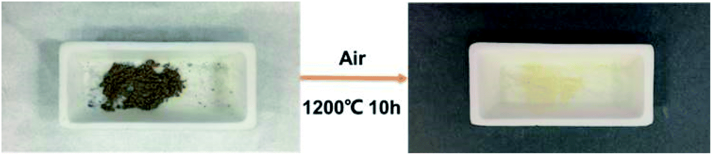 | ||
| Fig. 5 Comparison of Si@TiO2 before and after sintering in air. | ||
In order to study the electrochemical properties of the pure Si NPs and yolk–shell structured Si@TiN, galvanostatic charge–discharge tests were conducted on two samples in the voltage range of 0.01–2.5 V. Fig. 6a shows the first two charge–discharge curves of both materials at the current density of 400 mA g−1. The first discharge capacity of Si@TiN was 4200 mA h g−1 which is larger than that of 3916 mA h g−1 for the pure Si NP, and is more preponderant than the reported performance showing a specific capacity of 2634 mA h g−1 at a current density of 0.2 A g−1 in a bird's nest-like nanographene shell (NGS)-encapsulated Si@SiO2.23 It can be seen that the charging shapes of the two materials in the first two cycles are nearly similar, exhibiting the first discharge platform at around 0.1 V, which is a typical discharge characteristic for Si-based anodes.27 The second discharge plateau was significantly increased to above 0.4 V, which was caused by the structural change of Si from crystalline to amorphous phase after the first charge–discharge process,33 then the charging plateau was around 0.4 V for the two samples, which corresponds to the reaction of LixSi to the amorphous Si phase.34 Fig. 6b shows the cycling performance of the samples at the current density of 1000 mA g−1. It is noted that the two materials were pre-activated at the current density of 400 mA g−1 for 3 cycles to ensure the complete reaction of Si and Li during the initial electrochemical process. The discharge capacity of pure Si NPs rapidly decreased from 3398 to 189 mA h g−1 after 250 cycles, corresponding to a capacity retention of 5.5%. On the contrary, Si@TiN showed significantly improved cycle stability. A much larger discharge capacity of 1478 mA h g−1 was obtained after 500 cycles, resulting in significantly increased capacity retention. The improvements of electrochemical properties can be attributed to the following aspects. (1) The conductive TiN shell provides a continuous path for charge transfer along the active reaction sites and forms a homogeneous nanostructure to reduce the electric disconnection among active Si grains during cycling.35,36 (2) The void space reserved between the outer TiN shell and the inner Si core can effectively buffer the volumetric expansion and contraction of Si actives, thereby maintaining good electrical contact and preventing the disconnection of active Si particles from the Cu current collector.
 | ||
| Fig. 6 (a) The 1st and 2nd galvanostatic charge–discharge profiles, (b) cycling performance at a current density of 1000 mA g−1, and (c) rate performance of the Si NPs and Si@TiN samples. | ||
Fig. 6c shows the rate performance of the pure Si NPs and yolk–shell structured Si@TiN. It can be seen that the discharge capacities of Si NPs at the current densities of 0.4, 1, 2 and 4 A g−1 were 3916, 2567, 1913 and 1203 mA h g−1, respectively. When the current densities increased to 8 and 12 A g−1, Si NPs had almost no available capacity at these high current rates. In contrast, the discharge capacities of Si@TiN at the same current densities were 4011, 2962, 2612, 2085, 1360 and 903 mA h g−1, respectively, exhibiting excellent rate performance compared with pure-phase Si. In addition, when the current densities returned to 8, 4, 2, 1 and 0.4 A g−1, the reversible capacities could generally recover to the corresponding original values, which were much better than those of Si NPs because the pure Si NPs experienced irreversible structural pulverization but the unique yolk–shell structured Si@TiN helped to stabilize the morphology and framework of Si-based anodes. The increased rate performance may be deemed as a combined effect of the TiN matrix serving as a buffer layer to adapt the expansions in volume and possessing high conductivity; the former is more crucial than the latter, instead of the catalytic reaction in the currently prepared sample.
EIS analysis was performed to deeply understand the improved electrochemical performance of the yolk–shell structured Si@TiN. The Nyquist plots of the electrodes after the 3rd charge are displayed in Fig. 7a. The two semicircles in the high-to-medium frequency region are due to the SEI film and charge transfer process, respectively. The slope line in the low-frequency region is due to Li+ diffusion in the electrode.37,38 The SEI resistance (Rf) of the pure Si electrode is 164 Ω, which is much larger than that of Si@TiN (91 Ω), indicating that the side reactions of the Si electrode are more unstoppable during cycling, and the accumulation of the thick SEI film is one of the major factors leading to the large cell polarization, poor capacity retention and low rate capability. The values of charge transfer resistance (Rct) are nearly equal for the two samples as shown in Table 1. In addition, we further carried out the Nyquist plots of the electrodes after the 180th charge as shown in Fig. 7b. Si@TiN showed a charge transfer resistance (Rct) of 52 Ω, which is much smaller than that of the pure Si (338 Ω). The improved charge transfer of Si@TiN is closely related to its unique structure and high electrical conductivity of the TiN shell.
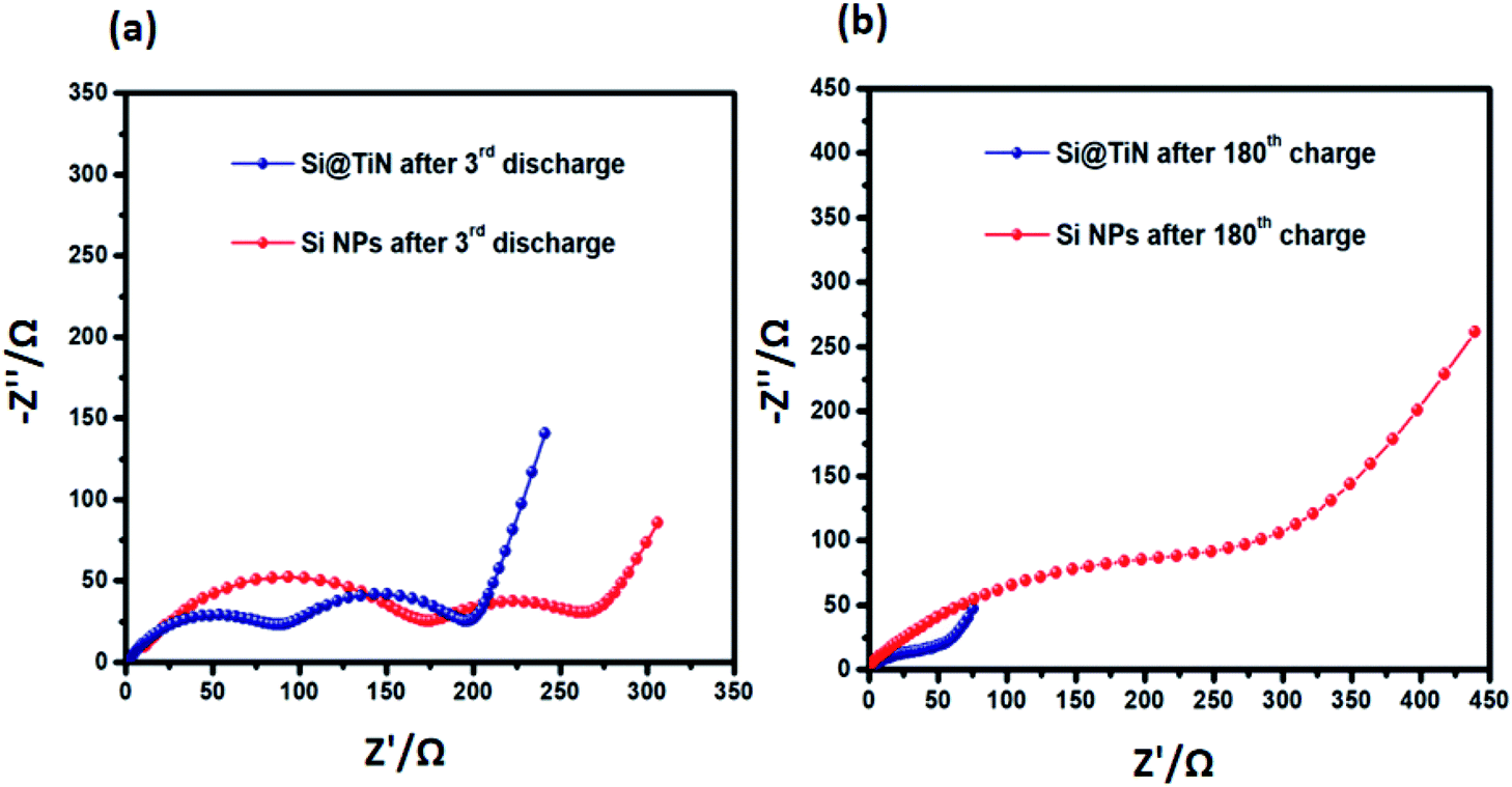 | ||
| Fig. 7 Nyquist plots of the Si NPs and Si@TiN after the (a) 3rd discharge and (b) 180th charge. | ||
| After the 3rd discharge | After the 180th charge | |||
|---|---|---|---|---|
| Si NPs | Si@TiN | Si NPs | Si@TiN | |
| Rf (Ω) | 164 | 93 | — | — |
| Rct (Ω) | 91 | 104 | 338 | 52 |
In order to observe whether the yolk–shell structure has an inhibitory effect on the volumetric expansion of Si, we conducted cross-sectional SEM tests on the electrodes of Si NPs and Si@TiN after different cycles as shown in Fig. 8. The electrode thicknesses of Si@TiN and Si NPs before cycling were 37.6 and 20.5 μm (Fig. 8a and d, respectively), and the values increased to 45.2 and 48.0 μm after the first discharge (Fig. 8b and e, respectively). Accordingly, the volumetric expansion of Si NPs was 134.1%, which is much larger than that of Si@TiN (20.2%). In addition, after the 180th charge, the thickness of the pure Si electrode increased to 66.9 from 20.5 μm, while the thickness of the Si@TiN electrode only increased to 39.0 from 37.6 μm as shown in Fig. 8c and f. It can be concluded from the results that the yolk–shell-structured Si@TiN significantly accommodates the volumetric change of the embedded Si particles during repeated alloying and de-alloying with lithium because of the existence of the void space and TiN matrix, and also prevents silicon nanoparticles from direct exposure to the electrolyte.
 | ||
| Fig. 8 Cross-sectional SEM images of (a–c) Si@TiN and (d–f) Si NPs before and after cycling. | ||
In order to confirm the morphology of the materials during charge–discharge cycling, the cell was disassembled after 180 cycles. The electrode composite was scraped off the current collector and completely washed with DMC to remove any appendages. TEM and HRTEM images of multiple particles for the pure Si NPs showed the visible pulverization and agglomeration of particles (Fig. 9c) as well as the apparent transformation to the amorphous phase (Fig. 9d), which could be attributed to the repeated intercalation and de-intercalation. Different from that observed for pure Si NPs, the boundary of the cycled Si@TiN as shown in Fig. 9a is much smoother and cleaner than that of the pristine Si, and the surface region could be indexed to the TiN phase as confirmed by its distinctive 111, 200 and 220 diffraction planes (Fig. 9b). However, no obvious Si-based regions were observed in the material bulk, indicating that Si NPs possibly became an amorphous structure with long-playing cycling.
 | ||
| Fig. 9 TEM and HRTEM images of (a and b) Si@TiN and (c and d) Si NPs after 180 cycles. | ||
Conclusion
In conclusion, a yolk–shell-structured Si@TiN composite has been successfully prepared by a feasible template method using phenolic resin. XRD, SEM and TEM have validated the composition, structure and morphology of the Si@TiN sample. The unique yolk–shell structure can not only reserve void space for the volumetric expansion of Si NPs during repeating cycling, but also help to improve the electronic conductivity of pure Si because of the conducting TiN shell. The EIS results showed that the SEI film resistance of Si@TiN is significantly lower than that of pure Si, indicating that the TiN shell is conducive to the formation of a stable SEI film for the electrode, ensuring the rapid transmission of Li+ at the surface and enabling the unhindered electrochemical dynamic kinetics. Finally, the cross-sectional SEM images of cycled Si NPs and Si@TiN also showed that the unique structure of Si@TiN not only reduces the volumetric expansion of the electrodes but also prevents the Si actives from falling off the collector current. Therefore, the above synergetic effects significantly improve the electrochemical performance of Si@TiN, which shows superior rate capability (the discharge capacity of 903 mA h g−1 at the high current density of 12 A g−1), and also good capacity retention (a high capacity of 1478 mA h g−1 after 500 cycles). The yolk–shell structure designed in this work will further promote the practical applications of Si-based anodes in lithium-ion batteries.Conflicts of interest
The authors declare no competing financial interest.Acknowledgements
This work was financially supported by the Research of Dongguan Science and Technology of Social Development Program (No. 20211800905482); Scientific Research Project of Guangdong University of Science and Technology (No. GKY-2021KYZDK-4); Project of Characteristic Innovation of Guangdong Province (No. 2021KTSCX148); 2021 Teaching Quality and Teaching Reform Project of Undergraduate Colleges and Universities in Guangdong Province (Yue Jiao Gao Han [2021] No. 29); Dongguan Sci-tech Commissioner Program (No. 20201800500592; No. 20201800500622).Notes and references
- S. Lawes, Q. Sun, A. Lushington, B. Xiao, Y. Liu and X. Sun, Nano Energy, 2017, 36, 313–321 CrossRef CAS.
- H. Song, H. X. Wang, Z. Lin, X. Jiang, L. Yu, J. Xu, Z. Yu, X. Zhang, Y. Liu, P. He, L. Pan, Y. Shi, H. Zhou and K. Chen, Adv. Funct. Mater., 2016, 26, 524–531 CrossRef CAS.
- Y. Xue, J. Deng, C. Wang, R. G. Mendes, L. Chen, Y. Xiao, Q. Zhang, T. Zhang, X. Hu, X. Li, M. H. Rümmeli and L. Fu, J. Mater. Chem. A, 2016, 4, 5395–5401 RSC.
- L. Zhang, H. Guo, R. Rajagopalan, X. Hu, Y. Huang, S. X. Dou and H. K. Liu, J. Mater. Chem. A, 2016, 4, 4056–4061 RSC.
- L. Zhang, R. Rajagopalan, H. Guo, X. Hu, S. Dou and H. Liu, Adv. Funct. Mater., 2016, 26, 440–446 CrossRef CAS.
- X. Zuo, J. Zhu, P. Müller-Buschbaum and Y.-J. Cheng, Nano Energy, 2017, 31, 113–143 CrossRef CAS.
- H. Seo, H.-S. Kim, K. Kim, H. Choi and J.-H. Kim, J. Alloys Compd., 2019, 782, 525–532 CrossRef CAS.
- C. Wang, Y. Han, S. Li, T. Chen, J. Yu and Z. Lu, ACS Appl. Mater. Interfaces, 2018, 10, 12750–12758 CrossRef CAS PubMed.
- Y. Deng, L. Ma, T. Li, J. Li and C. Yuan, ACS Sustainable Chem. Eng., 2018, 7, 599–610 CrossRef.
- O. Salihoglu and Y. E. Kahlout, Mater. Res., 2019, 22, 1–6 Search PubMed.
- G. Mu, Z. Ding, D. Mu, B. Wu, J. Bi, L. Zhang, H. Yang, H. Wu and F. Wu, Electrochim. Acta, 2019, 300, 341–348 CrossRef CAS.
- M. Ruttert, V. Siozios, M. Winter and T. Placke, Z. Anorg. Allg. Chem., 2019, 645, 248–256 CrossRef CAS.
- A. Sun, H. Zhong, X. Zhou, J. Tang, M. Jia, F. Cheng, Q. Wang and J. Yang, Appl. Surf. Sci., 2019, 470, 454–461 CrossRef CAS.
- Y. Chen, Y. Hu, Z. Shen, R. Chen, X. He, X. Zhang, Y. Li and K. Wu, J. Power Sources, 2017, 342, 467–475 CrossRef CAS.
- S. Guo, X. Hu, Y. Hou and Z. Wen, ACS Appl. Mater. Interfaces, 2017, 9, 42084–42092 CrossRef CAS PubMed.
- D. W. Kim, A. R. Park, T. S. Oh, N. E. Lee, P. J. Yoo and J. B. Yoo, J. Mater. Chem. A, 2017, 5, 14906–14913 RSC.
- L. Zhang, X. Hu, C. Chen, H. Guo, X. Liu, G. Xu, H. Zhong, S. Cheng, P. Wu, J. Meng, Y. Huang, S. Dou and H. Liu, Adv. Mater., 2017, 29, 1604708–1604715 CrossRef PubMed.
- W. Sun, L. Wan, X. Li, X. Zhao and X. Yan, J. Mater. Chem. A, 2016, 4, 10948–10955 RSC.
- H. Yoo, E. Park, H. Kim, J. Bae, H. Chang, H. D. Jang and H. Kim, Chem. Commun., 2016, 52, 8030–8033 RSC.
- N. Liu, H. Wu, M. T. McDowell, Y. Yao, C. Wang and Y. Cui, Nano Lett., 2012, 12, 3315–3321 CrossRef CAS PubMed.
- J. Zhu, T. Wang, F. Fan, L. Mei and B. Lu, ACS Nano, 2016, 10, 8243–8251 CrossRef CAS PubMed.
- X. Ding, X. Liu, Y. Huang, X. Zhang, Q. Zhao, X. Xiang, G. Li, P. He, Z. Wen, J. Li and Y. Huang, Nano Energy, 2016, 27, 647–657 CrossRef CAS.
- B. Li, Y. Jiang, F. Jiang, D. Cao, H. Wang and C. Niu, J. Power Sources, 2017, 341, 46–52 CrossRef CAS.
- Y. Dong, Y. Wu, M. Liu and J. Li, ChemSusChem, 2013, 6, 2016–2021 CrossRef CAS PubMed.
- J. A. Kwon, M.-S. Kim, D. Y. Shin, J. Y. Kim and D.-H. Lim, J. Ind. Eng. Chem., 2017, 49, 69–75 CrossRef CAS.
- W. Wen, J.-C. Yao, H. Tan and J.-M. Wu, J. Mater. Chem. A, 2019, 7, 21378–21385 RSC.
- W. Wen, Y.-N. Chen, S.-G. Wang, M.-H. Cao, J.-C. Yao, Y.-J. Gu and J.-M. Wu, Appl. Mater. Today, 2018, 12, 276–282 CrossRef.
- W. Wen, J.-M. Wu, Y.-Z. Jiang, L.-L. Lai and J. Song, Chem, 2017, 2, 404–416 CAS.
- X. Zhou, L. Wu, J. Yang, J. Tang, L. Xi and B. Wang, J. Power Sources, 2016, 324, 33–40 CrossRef CAS.
- J. Zhu, J. Yang, Z. Xu, J. Wang, Y. Nuli, X. Zhuang and X. Feng, Nanoscale, 2017, 9, 8871–8878 RSC.
- M.-S. Balogun, M. Yu, C. Li, T. Zhai, Y. Liu, X. Lu and Y. Tong, J. Mater. Chem. A, 2014, 2, 10825–10829 RSC.
- D. Tang, R. Yi, M. L. Gordin, M. Melnyk, F. Dai, S. Chen, J. Song and D. Wang, J. Mater. Chem. A, 2014, 2, 10375–10378 RSC.
- Z. Hou, X. Zhang, J. Liang, X. Lia, X. Yan, Y. Zhu and Y. Qian, RSC Adv., 2015, 5, 71355–71359 RSC.
- N. Lin, Y. Han, J. Zhou, K. Zhang, T. Xu, Y. Zhu and Y. Qian, Energy Environ. Sci., 2015, 8, 3187–3191 RSC.
- S. Cao, J. Bennett, Y.-K. Wang, S. Gracious, M. Zhu and M. N. Obrovac, J. Power Sources, 2019, 438, 22700 CrossRef.
- D. Kim, S. Park, J. Mun and J.-H. Ryu, Int. J. Energy Res., 2020, 44, 9233–9239 CrossRef CAS.
- Y. Fernández Pulido, C. Blanco, D. Anseán, V. M. García, F. Ferrero and M. Valledor, Measurement, 2017, 106, 1–11 CrossRef.
- Q.-C. Zhuang, X.-Y. Qiu, S.-D. Xu, Y.-H. Qiang and S.-G. Sun, Prog. Chem., 2010, 22, 1044–1057 CAS.
| This journal is © The Royal Society of Chemistry 2022 |