DOI:
10.1039/D2RA02030K
(Paper)
RSC Adv., 2022,
12, 16732-16744
Adsorption of gas molecules on buckled GaAs monolayer: a first-principles study
Received
29th March 2022
, Accepted 30th May 2022
First published on 6th June 2022
Abstract
The design of sensitive and selective gas sensors can be significantly simplified if materials that are intrinsically selective to target gas molecules can be identified. In recent years, monolayers consisting of group III–V elements have been identified as promising gas sensing materials. In this article, we investigate gas adsorption properties of buckled GaAs monolayer using first-principles calculations within the framework of density functional theory. We examine the adsorption energy, adsorption distance, charge transfer, and electron density difference to study the strength and nature of adsorption. We calculate the change in band structure, work function, conductivity, density of states, and optical reflectivity for analyzing its prospect as work function-based, chemiresistive, optical, and magnetic gas sensor applications. In this regard, we considered the adsorption of ten gas molecules, namely NH3, NO2, NO, CH4, H2, CO, SO2, HCN, H2S, and CO2, and noticed that GaAs monolayer is responsive to NO, NO2, NH3, and SO2 only. Specifically, NH3, SO2 and NO2 chemisorb on the GaAs monolayer and change the work function by more than 5%. While both NO and NO2 are found to be responsive in the far-infrared (FIR) range, NO shows better spin-splitting property and a significant change in conductivity. Moreover, the recovery time at room temperature for NO is observed to be in the sub-millisecond range suggesting selective and sensitive NO response in GaAs monolayer.
1 Introduction
With the increased emission of toxic gas molecules due to the rapid progress of industrialization, the detection of gas molecules is critical. In this regard, the design and fabrication of stable, sensitive, and selective gas sensing devices that can detect molecules at a part per billion (ppb) concentration is crucial. Traditional MOS devices have high selectivity but do not have high sensitivity for detection at low concentrations.1 To achieve high sensitivity, 2D materials with their high surface-to-volume ratio showed great promise facilitating sensing in concentration as low as 1 ppb.2,3 However, 2D materials such as graphene-based chemiresistive sensors lack selectivity.4 Plasmonic and photonic gas sensors are used to selectively detect and capture gas molecules to overcome this issue.5,6 However, if materials are found that are intrinsically selective towards certain gas molecules, that is, adsorbs only certain molecules or has a distinct electronic or optical response, then the design of gas sensing devices can be much simpler without the need of complex devices. Thus, first-principles studies predicting the gas adsorbing behavior of emerging two-dimensional materials for identifying potential 2D materials have become a vital step in taking gas sensor research forward. 2D materials such as graphene have been experimentally reported to be useful in the sensitive detection of gas molecules.7,8 Single-atom doping of MoS2 has been reported to increase sensitivity towards biomolecules such as dopamine.9 Various 2D materials have been theoretically predicted to be excellent candidates for gas sensing application, such as, graphene,10–14 Stanene,15,16 MoS2,17 SiC,18 GeS,19 GaN,20 InN21 etc. Monolayers consisting of group III–V elements have also been predicted to be excellent gas sensing materials in the literature.22–25 For instance, hexagonal BAs is predicted to be a good candidate for SO2 sensor,26 whereas InN monolayer has shown strong SO2 and NO2 adsorption.27 Recent reports on GaAs monolayer have demonstrated that it has high carrier mobility, tunable band gap, and strong second harmonic generation (SHG) response.28–30 However, the adsorption of gas molecules on low buckled GaAs monolayer has not been investigated yet. The success of III–V monolayers in gas sensing and gas capturing combined with the excellent electronic and optical properties of GaAs monolayer has prompted us to study the adsorption of gas molecules on GaAs monolayer.
Therefore, in this work, we performed first-principles calculations to find out the adsorption property of ten gas molecules (NH3, NO2, NO, CH4, H2, CO, SO2, HCN, H2S, CO2) on GaAs monolayer. NOx and SO2 are toxic gas molecules that are reported to cause respiratory problems, photochemical smog, and acid rain.31–36 Other toxic gas molecules such as H2S, and NH3 can cause burns in the skin, mouth, throat, and lungs and can even be life-threatening.37–39 On the other hand, detection of CO, HCN, CH4, and H2 is critical due to the dangers of carbon monoxide poisoning,40,41 inhibition of the consumption of oxygen by body tissues,42 accidental explosion,43–46 and coal mine accidents.47
Four adsorption sites have been considered for each gas, and adsorption energy has been calculated to determine the most energetically favorable configuration. The strength and nature of the adsorption have been elucidated by adsorption distance, Hirshfeld charge transfer, and electron density difference. The stability of GaAs monolayer upon gas adsorption has been examined by phonon dispersion calculations. The electronic structure of the gas analyte system was examined by partial density of states (PDOS) and band structure analysis. The prospect of the materials being used as a gas sensor has been investigated by calculating the work function, conductivity, reflectivity, magnetic moment, and recovery time of all the GaAs analyte systems. The next section explains the computational details and method.
2 Method and computational details
First-principles density function theory (DFT) has been used throughout this work. DFT calculations have been carried out using DMol3 (ref. 48) and CASTEP49 modules of Materials Studio. At first, a 3 × 3 supercell of GaAs monolayer was prepared by cleaving the bulk GaAs crystal, as shown in Fig. 1. A large vacuum slab of 21 Å was added to minimize spurious interaction with periodic images. The value of 21 Å is reported to be enough for accurate calculations of electronic and optical properties of GaAs monolayer.50 Substrates can impact the properties of a two-dimensional material. Previous reports show that metallic states can appear on the interface states between the substrate material, and atomic layer janus MoSSe.51 In gas or adatom adsorption, the presence of a substrate can enhance the adsorption energy and charge transfer between an adsorbent gas or dopant atom and the adsorbing material.52,53 However, the experimental performance of 2D material based gas sensors with substrate has been successfully predicted by modelling the free standing monolayer in DFT calculation in past studies.9,54 Hence, we used freestanding GaAs to model gas adsorption for less computational load.
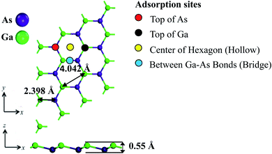 |
| | Fig. 1 Optimized structure of GaAs monolayer showing the lattice constant of 4.042 Å, bond length 2.398 Å, buckling height of 0.55 Å, and the four adsorption sites. | |
The obtained GaAs monolayer was relaxed using the DMol3 module until energy and force were converged to 1.0 × 10⁻⁷ Ha and 1.0 × 10⁻⁴ Ha per Å, respectively. The band structure, density of states, and Hirshfeld charge analyses of 3 × 3 supercell of the relaxed pristine GaAs monolayer were performed with DMol3 module while the optical properties and phonon spectra were obtained using the CASTEP module. Monkhorst-Pack grid of 10 × 10 × 1 and 16 × 16 × 1 were used for geometry optimization and electronic structure calculation, respectively. Fermi level smearing was taken as 0.005 Ha. Double numerical polarized plus (DNP+) basis set was used with a global orbital cutoff of 5.0 Å. Generalized gradient approximation (GGA) with Perdew–Burke–Ernzerhof functional was used in all calculations. Hybrid Heyd, Scuseria, Ernzerhoff (HSE06) functional provides band gap values that are in excellent agreement with the experimental values. However, in gas sensing, the change of band gap is more of interest than the absolute value of band gap. Hence, in accordance with the previous DFT studies on gas sensing, GGA-PBE functional was selected for computational efficiency.18,55 For dispersion correction, taking van der Waals interactions into account, DFT-D dispersion correction method provided by Grimme was used. Gas molecules were subsequently added to the considered initial adsorption sites to determine the most stable site of adsorption. The four chosen initial adsorption sites: Ga (top of Ga atom), As (top of As atom), hollow (top of the center of hexagon), and bridge (top of Ga–As bonds), are shown in Fig. 1. Furthermore, as can be seen from Fig. 1, the Ga (As) protrusion is upwards (downwards). This can lead to non-identical adsorption on both sides. Hence, we added the gas molecules to both sides. A comparison between adsorption energies of the gas molecules on Ga protruded side and As protruded side is summarized in Table 1. After the adsorption, these structures were relaxed using the same parameters used in the structural relaxation of the pristine monolayer. Then the adsorption energy and the charge transfer of gas adsorbed systems were calculated as follows:56
| | |
Ead = E(gas + GaAs) − E(GaAs) − E(gas)
| (1) |
| | |
Δρ = ρ(gas + GaAs) − ρ(GaAs) − ρ(gas)
| (2) |
Here
Ead,
E(gas),
E(gas + GaAs), and
E(GaAs) represent adsorption energy, the energy of the isolated adsorbate gas molecule, gas adsorbed GaAs monolayer, and pristine GaAs monolayer, respectively. A negative value of
Ead denotes strong exothermic interaction and thermally stable adsorption. The larger the absolute value of
Ead, the stronger the interaction. Only the most energetically favorable configurations were considered for the subsequent analysis.
ρ(gas + GaAs),
ρ(GaAs),
ρ(gas) are the charge on gas adsorbed GaAs monolayer, pristine GaAs monolayer, and gas molecule, respectively. The calculated adsorption energy from
eqn (1) is not a direct measure of experimental adsorption energy. Hence, zero point vibrational energy (ZPVE) was taken into account, and corrected adsorption energy,
E′
ad was also calculated according to the equation
E′
ad = (
E + ZPVE)
gas+GaAs − (
E + ZPVE)
gas − (
E + ZPVE)
GaAs. The dynamic stability of gas adsorption was also verified using phonon spectra calculations, and the supercell cutoff radius was selected to be 5 Å.
Table 1 Comparison between adsorption energy on Ga protruded side vs. As protruded side
| Gas |
Ga protruded side |
As protruded side |
| NH3 |
−0.88451 |
−0.59604 |
| NO2 |
−1.28484 |
−1.48732 |
| NO |
−0.44763 |
−0.27312 |
| H2 |
−0.10449 |
−0.10417 |
| CO |
−0.28088 |
−0.15979 |
| CH4 |
−0.19513 |
−0.18613 |
| SO2 |
−0.8167 |
−0.39242 |
| HCN |
−0.30572 |
−0.14357 |
| H2S |
−0.42689 |
−0.23032 |
| CO2 |
−0.13274 |
−0.13543 |
After verifying the stability of gas adsorption, the band structure and density of states calculation and the Hirshfeld charge analysis were performed on the gas adsorbed GaAs monolayers to determine the nature and mechanisms of gas adsorption. Finally, the gas sensing performance of GaAs monolayer was examined where, conductivity, reflectivity, magnetic moment, and work function were considered to be the sensing parameters.
3 Results and discussion
3.1 Benchmarking the simulation method and parameters
The electronic and structural properties were studied first to benchmark the simulation method and parameters and to study the change of electronic properties after gas adsorption. GaAs monolayer is found to be a low buckled monolayer with a bond length of 2.398 Å, lattice constant of 4.042 Å, and buckling height of 0.55 Å. The results are in agreement with previous theoretical studies.30,50,57 The band gap of GaAs monolayer is calculated to be 1.046 eV from the GaAs monolayer band structure (shown in Fig. 2), which is also in agreement with previous studies performed at the PBE level of theory.30 These results also serve as the reference for subsequent analyses on gas-adsorbed GaAs monolayer.
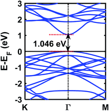 |
| | Fig. 2 The band structure of pristine GaAs monolayer with a band gap of 1.046 eV. | |
3.2 Adsorption configurations of gas molecules on GaAs monolayer
Geometry optimization was performed on all considered gas molecules and adsorbed configurations, and the corresponding adsorption energy was calculated. The most energetically favorable optimized structures that are considered for further analysis are shown in Fig. 3. As seen in Fig. 3, different gas molecules favor different adsorption sites, and the orientations of gas molecules are also disparate—some gas molecules get adsorbed with the molecules parallel to the GaAs monolayer surface. In contrast, other gas molecules get adsorbed with vertical or oblique orientation.
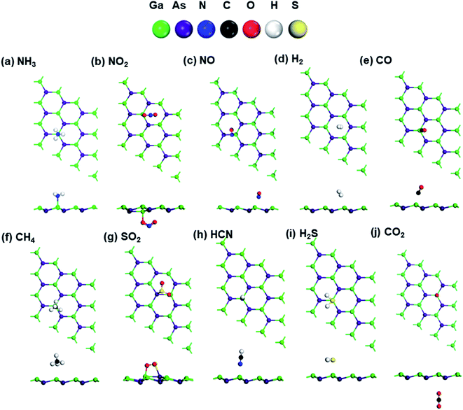 |
| | Fig. 3 Top and side view of the most energetically favorable adsorption configuration of the adsorbed molecules (a) NH3, (b) NO2, (c) NO, (d) H2, (e) CO, (f) CH4, (g) SO2, (h) HCN, (i) H2S, and (j) CO2 molecules on the GaAs monolayer. The balls of the colors green, violet, blue, red, black, yellow, and white represent Ga, As, N, O, C, S, and H. | |
The shortest distance from the gas molecule to the GaAs surface (D) is also observed to differ. The nature of bonding between the gas molecules and GaAs monolayer is influenced by this distance, D and it helps in understanding the nature of adsorption. The bonding was determined using the bond calculator tool of Materials Studio, which uses the criterion that D needs to be within the following range:
| | |
0.6 × Di < D < 1.15 × Di,
| (3) |
where
Di =
Rcov(Atom1) +
Rcov(Atom2) and
Rcov denotes the covalent radius of the atom.
The charge transfer and adsorption energy are also taken into account for determining the nature of adsorption. In general, adsorption energy of −0.5 eV or less (greater in absolute value) is required for chemisorption.58–60 The adsorption configurations and the nature of adsorption for the gas molecules are discussed in the following portion.
3.2.1 NH3. For NH3 adsorption on GaAs monolayer, the adsorption energy was calculated to be −0.76 eV, indicating highly energetically favorable adsorption. The preferred adsorption site was the top of the Ga atom on the Ga protruded side as can be seen from Fig. 3(a). NH3 molecule forms a Ga–N bond with a bond length of 2.138 Å. The calculated Hirshfeld charge transfer is 0.2433|e|. The Ga atom that bonded with the NH3 molecule has a charge of 0.274|e| on it, which can also be observed from the large charge depletion on the Ga atom that bonds with the NH3 molecule, as can be seen in Fig. 4(a). Large adsorption energy combined with high charge transfer indicates that NH3 molecule chemisorbs on GaAs monolayer.
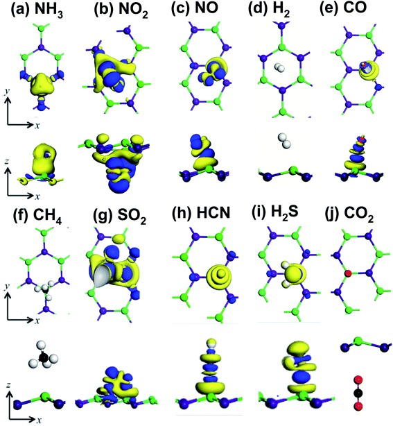 |
| | Fig. 4 Electron density difference plots of (a) NH3, (b) NO2, (c) NO, (d) H2, (e) CO, (f) CH4, (g) SO2, (h) HCN, (i) H2S, and (j) CO2 adsorbed GaAs monolayer. Here the blue (yellow) color denotes electron accumulation (depletion). Isovalue is 0.01 electrons per Å3. | |
3.2.2 NO2. In the case of NO2 adsorption, the NO2 molecule was observed to get adsorbed close to the top of the Ga atom of the As protruded side as seen in Fig. 3(b). In this case, oxygen atom of NO2 was directly above the Ga atom of GaAs monolayer with the NO2 molecule parallel to the GaAs monolayer. The Ga atom of GaAs monolayer formed a Ga–O bond with a bond length of 2.023 Å. The calculated adsorption energy was −1.46 eV which indicates highly energetically favorable adsorption. A high charge transfer of 0.2803|e| from GaAs to NO2 was also observed. In Fig. 4(b), the high charge accumulation on NO2 molecule and depletion on GaAs can be seen, which confirms the high charge transfer. The low adsorption distance, high charge transfer, and adsorption energy are indicative of chemisorption.
3.2.3 NO. The most stable adsorption site for the NO molecule was observed to be the bridge site of the Ga protruded side, although the NO molecule was not in the exact center of the Ga–As bond. Instead, the NO molecule was closer to the top of the Ga atom than the top of the As atom, as shown in Fig. 3(c). Adsorption energy was found to be −0.39 eV, and the calculated adsorption distance was 2.188 Å. No bond formation between the NO molecule and GaAs monolayer was observed. However, a moderately high charge transfer of 0.18|e| was noted. The charge accumulation on the N atom of NO molecule and charge depletion on GaAs monolayer can be seen in Fig. 4(c). Nonetheless, an |adsorption energy| less than |0.5| eV with a large adsorption distance is indicative of physisorption. Hence, it can be concluded that NO molecule is physisorbed on GaAs monolayer.
3.2.4 H2. From Fig. 3(d), it can be seen that the most stable site for the H2 molecule on GaAs monolayer was the hollow site of the Ga protruded side. Adsorption energy was −0.07 eV. Very low adsorption energy is indicative of weak adsorption. Charge transfer was also low: 0.045|e|, when H2 molecule was adsorbed on GaAs monolayer. The electron density difference plot in Fig. 4(d) shows no perceptible charge accumulation or depletion. The adsorption distance was 3.155 Å. The low adsorption energy, high adsorption distance, and negligible charge transfer confirm the physisorption of H2 molecules on GaAs monolayer.
3.2.5 CO. CO molecule was adsorbed on top of the Ga atom with the carbon atom close to the Ga atom of the Ga protruded side, as can be seen in Fig. 3(e). Adsorption energy was −0.24 eV. A moderate Hirshfeld charge transfer of 0.0081|e| was calculated. The charge transfer can also be observed from the charge depletion on GaAs monolayer surface and charge accumulation on the CO molecule, as shown in Fig. 4(e). The adsorption distance was large—2.147 Å, and no bond formation was detected. Because of the low adsorption energy and long adsorption distance, we can conclude the CO physisorbed on GaAs monolayer.
3.2.6 CH4. In the case of CH4 adsorption, as shown in Fig. 3(f), the most stable adsorption site was the Ga site of the Ga protruded side. Adsorption energy was −0.21 eV. Very low adsorption energy is indicative of very weak adsorption. Adsorption distance was 3.006 Å while the charge transfer was 0.09|e|. The low charge transfer is also evident from Fig. 4(f) where no charge accumulation or depletion can be seen. A high adsorption distance means that only weak van der Waals attraction existed between the CH4 molecule and GaAs monolayer. These results indicate that although GaAs monolayer might not be appropriate for CH4 adsorption, GaAs monolayer was unaffected by CH4 molecule, which means that CH4 molecule might not inhibit the sensing performance in the case of other molecules.
3.2.7 SO2. The most energetically preferable site of adsorption for SO2 was observed to be the bridge site of the Ga protruded side. The S atom of SO2 bonded with the As atom while the O atom bonded with the Ga atom as can be seen from Fig. 3(g). The shortest distance between the SO2 atom and GaAs monolayer surface was 1.954 Å. The adsorption energy was calculated to be −0.78 eV. Hirshfeld charge transfer indicates that 0.2643|e| transferred from GaAs monolayer to the SO2 monolayer. A large amount of charge piling up between SO2 and GaAs monolayer is presented in Fig. 4(g). The large charge transfer along with the high adsorption energy and low adsorption distance indicates that SO2 chemisorbed on GaAs monolayer.
3.2.8 HCN. The most stable site for HCN adsorption on GaAs monolayer, was the Ga site of the Ga protruded side as can be seen in Fig. 3(h). The HCN molecule was vertical and the distance between the N atom and Ga atom was 2.313 Å. The calculated adsorption energy was −0.25 eV and the Hirshfeld charge transfer was 0.1643|e|. A moderate amount of charge depletion was observed between the N atom of HCN and GaAs monolayer which can be observed in Fig. 4(h). Charge accumulation was observed between the C atom and N atom of the HCN molecule. Since the absolute value of adsorption energy was lower than 0.5 eV and the adsorption distance was high, it can be concluded that the HCN molecule physisorbed on the GaAs monolayer.
3.2.9 H2S. The most stable site for H2S molecule was the Ga site of the Ga protruded side. The H2S molecule was parallel to the GaAs monolayer surface with the S atom on top of the Ga atom as presented in Fig. 3(i). The distance between the Ga atom and the S atom on top of the Ga atom was 2.646 Å. The calculated adsorption energy was −0.34 eV. The Hirshfeld charge transfer was calculated to be 0.1897|e|. Charge accumulation on the S atom and depletion on the Ga atom can be seen in Fig. 4(i). The large adsorption distance and low adsorption energy suggest that H2S molecule physisorbed on the GaAs monolayer.
3.2.10 CO2. The CO2 molecule was adsorbed on the Ga site of the As protruded side with the CO2 molecule vertical to the GaAs monolayer as can be seen in Fig. 3(j). The calculated adsorption energy was very low −0.1211 eV. The adsorption distance between the CO2 molecule and GaAs monolayer was 3.413 Å. Furthermore, the Hirshfeld charge transfer between the CO2 molecule and GaAs monolayer was 0.0081|e|. No charge piling between the CO2 molecule and GaAs monolayer was observed as shown in Fig. 4(j). The low adsorption energy, high adsorption distance, and low charge transfer indicate that CO2 molecule physisorbed on the GaAs monolayer.The difference between the GaAs—analyte systems, the adsorption energy (Ead), adsorption distance (D), and Hirshfeld charge transfer (Q) are summarized in Table 2. As can be seen from Table 2, NH3, NO2, and SO2 are chemisorbed on GaAs monolayer while the other gas molecules are physisorbed.
Table 2 Adsorption energy (Ead), ZPVE corrected adsorption energy (E′ad) adsorption distance (D), and Hirshfeld charge transfer (Q) of the most energetically favorable gas adsorbed structures. A negative value of Q indicates charge transfer from GaAs to the gas molecule
| Gas molecule |
Ead (eV) |
E′ad (eV) |
Q (|e|) |
D (Å) |
Type of adsorption |
| NH3 |
−0.8845 |
−0.7563 |
0.2433 |
2.138 |
Chemisorption |
| NO2 |
−1.4874 |
−1.4643 |
0.2803 |
2.023 |
Chemisorption |
| NO |
−0.4476 |
−0.3889 |
−0.18 |
2.188 |
Physisorption |
| H2 |
−0.1044 |
−0.0741 |
0.045 |
3.155 |
Physisorption |
| CO |
−0.2808 |
−0.2383 |
0.11 |
2.147 |
Physisorption |
| CH4 |
−0.1951 |
−0.2091 |
−0.09 |
3.006 |
Physisorption |
| SO2 |
−0.8167 |
−0.7843 |
−0.2643 |
1.954 |
Chemisorption |
| HCN |
−0.3057 |
−0.2527 |
0.1643 |
2.313 |
Physisorption |
| H2S |
−0.4269 |
−0.3421 |
0.1897 |
2.646 |
Physisorption |
| CO2 |
−0.1354 |
−0.1211 |
0.0081 |
3.413 |
Physisorption |
3.3 Stability of the GaAs-analyte systems
Before studying the electronic and optical properties of the various gas adsorbed systems, the phonon spectra of the gas adsorbed systems were calculated to verify the dynamic stability of the gas adsorption. No imaginary frequency was observed in the case of the adsorption of any of the gas molecules except CH4 (Fig. 5(f)). Hence, CH4 adsorption was not considered in any of the subsequent calculations.
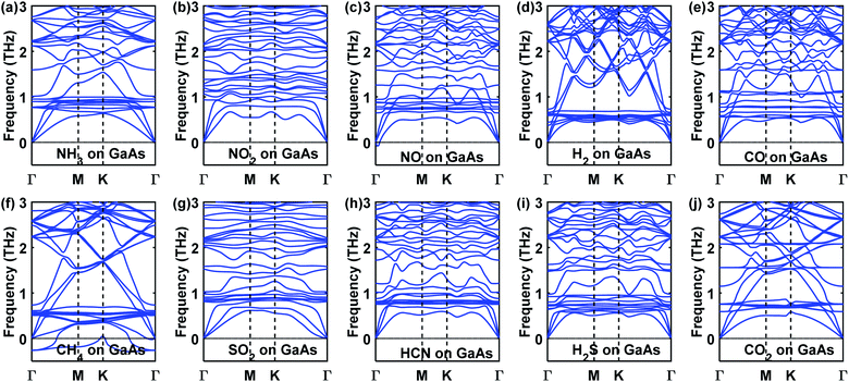 |
| | Fig. 5 Phonon dispersion curves of (a) NH3, (b) NO2, (c) NO, (d) H2, (e) CO, (f) CH4, (g) SO2, (h) HCN, (i) H2S, and (j) CO2 adsorbed GaAs monolayer. | |
3.4 The electronic structure of GaAs-analyte systems
The presence of gas molecules is expected to alter the electronic structures of GaAs monolayer. Hence, the orbital projected density of states and band structures were calculated. In Fig. 6 the band structures of all the gas adsorbed systems are presented. It can be seen from Fig. 6(b and e) that the effect of NH3 and H2 on the electronic properties of GaAs monolayer is negligible. The observed change in band gap was very small.
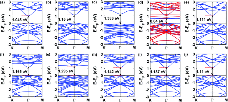 |
| | Fig. 6 The band structures of (a) pristine, and (b) NH3, (c) NO2, (d) NO, (e) H2, (f) CO, (g) SO2, (h) HCN, (i) H2S, and (j) CO2 adsorbed GaAs monolayer. The blue (red) color indicates up (down) spin. NO adsorption substantially decreases the band gap to 0.64 eV, while other gas adsorbed structures have a band gap reasonably similar to the pristine band gap of 1.046 eV. | |
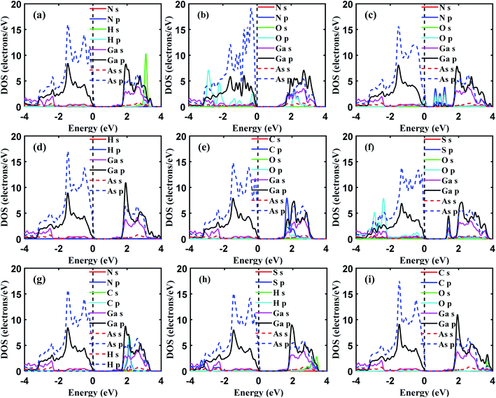
To understand the contribution of gas molecules in the electronic structure of the GaAs analyte systems, the projected density of states of the gas adsorbed structures was calculated. The N and H atoms of NH3 or H2 molecules have negligible contributions to the density of states, as seen in Fig. 7(a and d). However, when CO was adsorbed on the GaAs monolayer, a sizable change of 0.12 eV in the band gap was observed which can be seen in Fig. 6(f). Strong hybridization of p orbitals in the carbon atom, oxygen atom, and Ga atoms is observed at the 1.7–2 eV range, as can be seen in Fig. 7(e). This hybridization might have caused the conduction band to shift, which could have led to the change in band gap.
 |
| | Fig. 7 The orbital projected density of states of (a) NH3, (b) NO2, (c) NO, (d) H2, (e) CO, (f) SO2, (g) HCN, (h) H2S, and (i) CO2 adsorbed GaAs monolayer. The blue (red) color indicates up (down) spin. NO adsorption substantially decreases the band gap to 0.64 eV, while other gas adsorbed structures have a band gap reasonably similar to the pristine band gap of 1.046 eV. | |
Strong hybridization also occurred when NO was adsorbed on GaAs. In this case, the hybridization occurred between p orbitals of N and O atoms. NO adsorption also gave rise to new states, as seen in Fig. 7(c). Because the new states arrived at the 0.5 to 1.5 eV region, the band gap decreased the most to 0.64 eV when NO was adsorbed, as can be seen in Fig. 6(d). Like NO adsorption, new states also appear when NO2 gets adsorbed on the GaAs monolayer. Furthermore, strong hybridization between the orbitals of NO and GaAs was observed. In Fig. 7(b), it can be seen that p orbitals of N and O atoms hybridize with s and p orbitals of Ga and As around the 2 to 4 eV range. Furthermore, p orbitals of oxygen atoms hybridize with p orbitals of As and Ga atoms around −2 to −3 eV. Additionally, the orbital contribution from As atoms is higher than other gas adsorbed structures around 0 eV to −1 eV. So, the total density of states gets altered in the aforementioned ranges. The conduction band gets pushed upwards due to the interaction with NO2 molecules and consequently the band gap increases by 0.34 eV. SO2 adsorption altered the electronic structure of GaAs monolayer and increased the band gap to 1.295 eV as can be seen in Fig. 6(g). Strong hybridization between the p orbitals of Ga, O, and S atoms was observed in the 1.5 eV to 2 eV range in the conduction band. Furthermore, like NO2 adsorption, SO2 adsorption alters the density of states in the −2 to −4 eV range in the valence band. The p orbitals of O atom were observed to hybridize with p orbitals of Ga and As atoms (Fig. 7(f)). Hence two extra states were observed in the band structure in the −2 to −3 eV range as can be seen in Fig. 6(g). On the contrary, H2S adsorption did not alter the electronic structure of the GaAs monolayer. However, weak hybridization between the S and Ga atoms can be observed in the −2 to −4 eV range in the valence band as can be seen in Fig. 7(h). The band gap change was small (∼0.09 eV). On the other hand, HCN adsorption modified the electronic structure of GaAs monolayer. As can be seen in Fig. 7(g), the p orbitals of the C atom in HCN molecule hybridized strongly with the p orbitals of the Ga atom in the 1.8 eV to 2.2 eV range in the conduction band. HCN adsorption resulted in a change of 0.097 eV as can be seen in Fig. 6(h). CO2 adsorption did not alter the electronic structure of the GaAs monolayer much and the change in band gap was very small eV (∼0.07 eV) as can be seen in Fig. 6(j).
3.5 Gas sensing performance of GaAs monolayer
In this section, we discuss the gas sensing possibilities utilizing different properties of GaAs monolayer. Different properties can be utilized for sensing, such as work function, band gap change, optical response, and magnetic moment.61–65 We discuss each of them based on three main criteria: sensitivity, selectivity, and recovery time.
3.5.1 The prospect of GaAs monolayer in work function-based sensor. The work function (Φ) is an important property for optoelectronic devices. Furthermore, the work function of GaAs monolayer will dictate its Schottky barrier height with various metal electrodes and graphene electrodes. The work function of the pristine GaAs monolayer was calculated to be 5.143 eV. The work function of the gas adsorbed structures was then calculated. The work functions of the gas adsorbed GaAs monolayer are shown in Table 3. In Table 3, ΔΦ is defined as the difference between the work function of the gas adsorbed structure and pristine GaAs, i.e., ΔΦ = ΦGaAs+gas − ΦGaAs. The sensitivity, S, is defined as S = |ΔΦ/ΦGaAs| × 100.
Table 3 The work functions of the gas adsorbed GaAs monolayer. GaAs monolayer has a sensitivity greater than 5% towards NH3 and NO2
| Adsorbed gas |
Φ (eV) |
ΔΦ (eV) |
S (%) |
| NH3 |
4.842 |
−0.301 |
5.85 |
| NO2 |
5.522 |
0.379 |
7.37 |
| NO |
5.196 |
0.053 |
1.03 |
| H2 |
5.196 |
0.053 |
1.03 |
| CO |
5.196 |
0.053 |
1.03 |
| SO2 |
5.415 |
0.272 |
5.29 |
| HCN |
4.789 |
−0.354 |
6.88 |
| H2S |
5.034 |
−0.109 |
2.12 |
| CO2 |
5.007 |
0.136 |
2.64 |
The work functions of NO, CO, and H2 adsorbed GaAs monolayer was calculated to be 5.196 eV. The change in work function is not large in any of these cases. On the contrary, the work function of the NH3, NO2, SO2, and HCN adsorbed GaAs monolayer were 4.842 eV, 5.522 eV, 5.42 eV, and 4.789 eV, respectively. The calculated sensitivity was greater than 5% for all these cases. Hence, GaAs monolayer could be a sensitive material for NH3, NO2, SO2, and HCN detection in work-function based sensors.
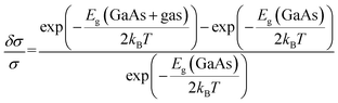
3.5.2 The prospect of GaAs monolayer in chemiresistive sensors. The conductivity was calculated using the relation,66,67, 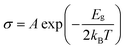 . Here, A is a proportionality constant, Eg is the band gap of the pristine or gas adsorbed structure, kB is the Boltzmann constant, and T is the temperature. The change of conductivity can thus be used to define sensitivity and can be expressed as
| |
 | (4) |
The calculated sensitivity is shown in Table 4.
Table 4 The sensitivity of GaAs monolayer towards different gas molecules
| Gas molecule |
Sensitivity |
| NH3 |
0.86 |
| NO2 |
0.99 |
| NO |
2.54 × 10³ |
| H2 |
0.71 |
| CO |
0.90 |
| SO2 |
0.99 |
| HCN |
0.84 |
| H2S |
0.83 |
| CO2 |
0.698 |
Since NO adsorbed GaAs monolayer has the greatest change in band gap, which is, 0.405 eV, the sensitivity of GaAs monolayer is the highest towards NO, which is 2.54 × 10³. The band gap change is less than 0.34 eV, and the sensitivity is less than 1 in the case of all other molecules. Hence, GaAs could be used in chemiresistive sensors for selective detection of NO.
3.5.3 The prospect of GaAs monolayer in optical gas sensors. Optical gas sensors have gained popularity recently.68–70 The change of optical properties such as absorption coefficient, reflectivity, dielectric function in the presence of gas molecules could be used for selective gas sensing. The benefit of optical gas sensors is that by tuning the sensor to different frequencies, the same material could be used for selective detection of different molecules. The reflectivity of GaAs monolayer was calculated before and after the gas adsorption of the considered molecules. The variation of reflectivity with respect to photon energy is presented in Fig. 8, where the incident light is perpendicular to the monolayer. The reflectivity of GaAs monolayer was sensitive towards NO and NO2 molecules in the far-infrared (FIR) range as can be seen in Fig. 8.
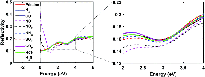 |
| | Fig. 8 The reflectivity of pristine and gas adsorbed GaAs monolayer. The reflectivity of NO and NO2 adsorbed monolayers are higher than the pristine and other gas adsorbed monolayers in the 0–1 eV range. In the 4–6 eV range, the reflectivity curves are on top of each other, indicating that the value of reflectivity is the same for all structures in this range. | |
The reflectivity of GaAs monolayer was calculated to be 0.1 in the 0 to 1 eV range, whereas the reflectivity of NO and NO2 adsorbed GaAs monolayer were much higher, ranging from 0.4 to 0.12 in the 0 to 0.5 eV range. The reflectivity of NO and NO2 adsorbed GaAs monolayers are distinct from each other too, which means that they can be distinctly detected. Furthermore, the reflectivity of NO and NO2 adsorbed monolayers were less than the pristine monolayer in the visible range. At 2 eV, the reflectivity of the pristine monolayer was approximately 0.16, whereas the reflectivity of NO and NO2 adsorbed GaAs monolayer was 0.13 and 0.14 respectively. These results indicate that GaAs monolayer could work as a selective and sensitive gas sensor in the visible range too.
3.5.4 The prospect of GaAs monolayer in magnetic gas sensors. Magnetic gas sensors have gained popularity in recent times due to their safety and lack of electrical contacts.71–73 Hence, the prospect of GaAs monolayer as a magnetic gas sensor has been explored. Spin-polarized DFT calculations were performed to analyze the magnetic moment of the gas adsorbed systems. It was found that magnetic moment was induced on GaAs monolayer when NO molecule was adsorbed on it. From the band structure plot in Fig. 6(e), it can be seen that magnetization occurred, which is indicated by the split of up spin and down spin conduction bands. The induced magnetism was further confirmed by the asymmetry in the up spin and down spin density of states as shown in Fig. 9(a). The induced magnetic moment was 1.02 μB. The spin density isosurface shown in Fig. 9(b) also confirms the induced magnetism. It can be seen that the magnetic moment is induced in the arsenic atoms adjacent to the adsorption site. It is to be noted that the magnetic moment is only induced when NO molecule is adsorbed on the GaAs monolayer surface. In all other cases, the GaAs—analyte system is non-magnetic. This distinct behavior towards NO molecule indicates that GaAs monolayer could be used as a magnetic gas sensor. The selectivity may be better than the previously reported cases where the magnetic moment was induced by multiple gas molecules.20,74
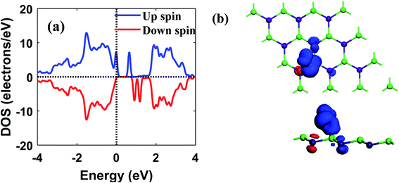 |
| | Fig. 9 (a) Spin resolved density of states in NO adsorbed GaAs monolayer; (b) the isosurface of showing spin density in NO adsorbed GaAs monolayer. Blue color represents up spin and red represents down spin. Isovalue is 0.005e per Angstrom3. | |
3.5.5 Recovery time. Recovery time is defined as the time required for an adsorbed gas molecule to spontaneously desorb from the adsorption surface. It is a crucial parameter that indicates the reusability of a gas sensor. The recovery time was calculated using the van't Hoff-Arrhenius equation,75 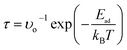 , where υo is the attempt frequency. Previous reports determined the attempt frequency of NO2 to be 1012 s−1.76 According to previous works, it is reasonable to assume the same attempt frequency for other gas molecules.18,77,78 The considered temperature was 300 K. The recovery times at temperatures 300–600 K are summarized in Table 5.
Table 5 The recovery time after gas adsorption for 300–600 K
| Gas molecule |
Recovery time (s) at 300 K |
Recovery time (s) at 400 K |
Recovery time (s) at 500 K |
Recovery time (s) at 600 K |
| NH3 |
5.38 |
0.0035 |
4.35 × 10⁻⁵ |
2.32 × 10⁻⁶ |
| NO2 |
4.45 × 10¹² |
3.07 × 10⁶ |
615.52 |
2.11 |
| NO |
3.52 × 10⁻⁶ |
8.13 × 10⁻⁸ |
8.471 × 10⁻⁹ |
1.88 × 10⁻⁹ |
| H2 |
1.77 × 10⁻¹¹ |
8.62 × 10⁻¹² |
5.601 × 10⁻¹² |
4.20 × 10⁻¹² |
| CO |
1.03 × 10⁻⁸ |
1.02 × 10⁻⁹ |
2.55 × 10⁻¹⁰ |
1.01 × 10⁻¹⁰ |
| SO2 |
15.93 |
0.008 |
8.34 × 10⁻⁵ |
3.99 × 10⁻⁶ |
| HCN |
1.79 × 10⁻⁸ |
1.55 × 10⁻⁹ |
3.57 × 10⁻¹⁰ |
1.34 × 10⁻¹⁰ |
| H2S |
5.74 × 10⁻⁷ |
2.08 × 10⁻⁸ |
2.85 × 10⁻⁹ |
7.57 × 10⁻¹⁰ |
| CO2 |
1.09 × 10⁻¹⁰ |
3.38 × 10⁻¹¹ |
1.67 × 10⁻¹¹ |
1.05 × 10⁻¹¹ |
The room temperature recovery time was calculated to be less than a millisecond for all of the gas adsorption cases except NH3 and NO2. However, in high temperatures such as 400 K, the recovery time for NH3 is less than a second. At 450 K, the recovery time for NO2 is approximately 4.6 hours, which is reasonable.18,66 At 500 K, the recovery time for NO2 gets down to 615.32 seconds, which is a rapid recovery time.79 Based on these results, it can be concluded that GaAs monolayer could be a suitable candidate for reusable gas sensors.
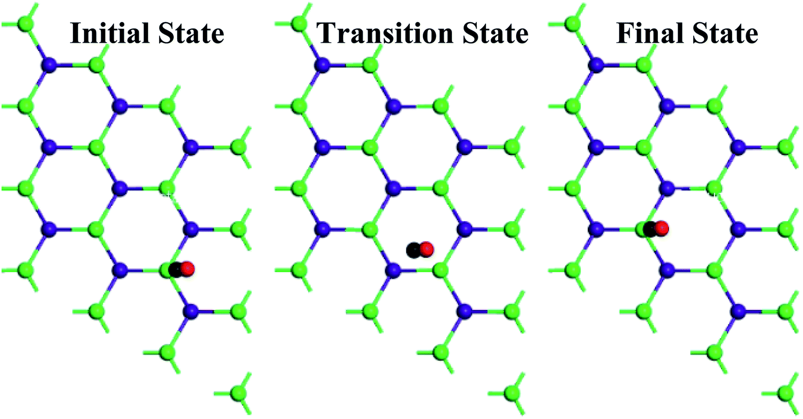
3.5.6 Diffusion analysis. Gas diffusion on the adsorbent surface is an important factor in gas sensor performance.80,81 Hence we calculated the diffusion of gas molecules on GaAs monolayer. We calculated the diffusion using the transition state search algorithm of DMol3 which performs a Linear Synchronous Transit (LST), followed by repeated conjugate gradient minimizations and Quadratic Synchronous Transit (QST) maximizations until a transition state has been located. To determine the diffusion barrier (Ebar), we set an initial structure (which is the relaxed structure in our study), and an equivalent structure where the gas molecule is adsorbed on a neighboring equivalent site as demonstrated in Fig. 10 for CO as an example. The transition state search algorithm then generated the diffusion pathway, transition state, and barrier energy. The diffusion barriers are summarized in Table 6.
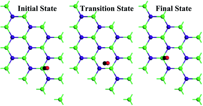 |
| | Fig. 10 Initial, transition, and final state for CO diffusion on GaAs monolayer. | |
Table 6 Diffusion barrier for the considered gas molecules
| Gas |
Ebar (eV) |
| NH3 |
0.67 |
| NO2 |
2.35 |
| NO |
0.33 |
| H2 |
0.08 |
| CO |
0.25 |
| CH4 |
0.12 |
| SO2 |
0.67 |
| HCN |
0.24 |
| H2S |
0.27 |
| CO2 |
0.08 |
As can be seen in Table 6, H2 and CO2 can diffuse easily on the GaAs surface. The rest of the gas molecules have a higher diffusion barrier. However, the calculated diffusion barriers are comparable to the diffusion barriers of various gas molecules on TiO2 nanoparticles.82
4 Conclusion
The prospect of buckled GaAs monolayer as a gas-sensing 2D material was systematically investigated using density functional theory. It was found that NH3, SO2, and NO2 molecules chemisorb while NO, CO, H2, HCN, CO2, and H2S molecules physisorb on the GaAs monolayer. Our calculations show that NH3 and HCN adsorption decreases the work function by 5.85% and 6.88%, while NO2 and SO2 adsorption increases the work function by 7.37% and 5.29% respectively. The adsorption of other gas molecules was observed to have minimal impact on the work function. It was also observed that NO adsorption decreases the band gap from 1.046 eV to 0.64 eV while the other gas molecules cause only very small changes. The calculated sensitivity of 2.54 × 10³ towards NO molecule suggests that GaAs monolayer could be a promising material for chemiresistive gas sensing. The induced magnetic moment was also investigated for all cases, and only NO adsorption was found to induce a magnetic moment of 1.02 μB. Hence, apart from chemiresistive sensing, GaAs monolayer could also be used in magnetic sensors for selective detection of NO molecules. Optical reflectivity analysis shows that adsorption of NO and NO2 increases the reflectivity of GaAs monolayer by 400% and 300%, respectively suggesting possible use in optical gas sensors. In summary, our results indicate that GaAs monolayer holds good prospects as chemiresistive, magnetic and optical sensors for sensitive and selective detection of NO with rapid recovery time.
Data availability
Source data are available from the corresponding author upon request.
Conflicts of interest
There are no conflicts of interest to declare.
Acknowledgements
We acknowledge the computational resources of the Department of Electrical and Electronic Engineering, Bangladesh University of Engineering and Technology.
Notes and references
- V. Salimian Rizi, F. Sharifianjazi, H. Jafarikhorami, N. Parvin, L. Saei Fard, M. Irani and A. Esmaeilkhanian, Mater. Res. Express, 2019, 6, 1150g2 CrossRef.
- W. Yuan and G. Shi, J. Mater. Chem. A, 2013, 1, 10078–10091 RSC.
- W. Tian, X. Liu and W. Yu, Appl. Sci., 2018, 8, 1118 CrossRef.
- J. Cao, Q. Chen, X. Wang, Q. Zhang, H.-D. Yu, X. Huang and W. Huang, Research, 2021, 2021, 1–38 CrossRef PubMed.
- M. R. Masuk, M. F. Hossain and J. Mahadi, IEEE Int. Conf. Telecommun. Photonics, Dhaka, Bangladesh, 2021, 1–4 Search PubMed.
- K. Khaliji, S. R. Biswas, H. Hu, X. Yang, Q. Dai, S. H. Oh, P. Avouris and T. Low, Phys. Rev. Appl., 2020, 13, 1–6 Search PubMed.
- M. D. Pedowitz, S. Kim, D. I. Lewis, B. Uppalapati, D. Khan, F. Bayram, G. Koley and K. M. Daniels, J. Microelectromech. Syst., 2020, 29, 846–852 CAS.
- A. Salehi-Khojin, D. Estrada, K. Y. Lin, M. H. Bae, F. Xiong, E. Pop and R. I. Masel, Adv. Mater., 2012, 24, 53–57 CrossRef CAS PubMed.
- Y. Lei, D. Butler, M. C. Lucking, F. Zhang, T. Xia, K. Fujisawa, T. Granzier-Nakajima, R. Cruz-Silva, M. Endo, H. Terrones, M. Terrones and A. Ebrahimi, Sci. Adv., 2020, 6, 1–10 Search PubMed.
- D. Zhao, X. Fan, Z. Luo, Y. An and Y. Hu, Phys. Lett. A, 2018, 382, 2965–2973 CrossRef CAS.
- G. Lu, S. Park, K. Yu, R. S. Ruoff, L. E. Ocola, D. Rosenmann and J. Chen, ACS Nano, 2011, 5, 1154–1164 CrossRef CAS PubMed.
- W. Yuan and G. Shi, J. Mater. Chem. A, 2013, 1, 10078–10091 RSC.
- C. Yi, W. Wang and C. Shen, AIP Adv., 2014, 4, 031330 CrossRef.
- F. Schedin, A. K. Geim, S. V. Morozov, E. W. Hill, P. Blake, M. I. Katsnelson and K. S. Novoselov, Nat. Mater., 2007, 6, 652–655 CrossRef CAS PubMed.
- A. Zhang, H. Yang, Q. Liu, W. Li and Y. Wang, Synth. Met., 2020, 266, 116441 CrossRef CAS.
- T. Wang, R. Zhao, M. Zhao, X. Zhao, Y. An, X. Dai and C. Xia, J. Mater. Sci., 2017, 52, 5083–5096 CrossRef CAS.
- Q. Yue, Z. Shao, S. Chang and J. Li, Nanoscale Res. Lett., 2013, 8, 1–7 CrossRef PubMed.
- Z. Zhao, Y. Yong, Q. Zhou, Y. Kuang and X. Li, ACS Omega, 2020, 5, 12364–12373 CrossRef CAS PubMed.
- S. Ma, D. Yuan, Y. Wang and Z. Jiao, J. Mater. Chem. C, 2018, 6, 8082–8091 RSC.
- Y. Yong, X. Su, H. Cui, Q. Zhou, Y. Kuang and X. Li, ACS Omega, 2017, 2, 8888–8895 CrossRef CAS PubMed.
- Adsorption of gas molecules on graphene-like InN monolayer: a first-principle study – ScienceDirect, https://www.sciencedirect.com/science/article/abs/pii/S0169433217302878, accessed 17 February 2021 Search PubMed.
- G. Wang, J. Yu, K. Zheng, Y. Huang, X. Li, X. Chen and L. Q. Tao, IEEE Electron Device Lett., 2020, 41, 1404–1407 CAS.
- S. Ma, D. Li, X. Rao, X. Xia, Y. Su and Y. Lu, Adsorption, 2020, 26, 619–626 CrossRef CAS.
- L. Lin, T. Liu, Y. Zhang, R. Sun, W. Zeng and Z. Wang, Ceram. Int., 2016, 42, 971–975 CrossRef CAS.
- C. Feng, H. Qin, D. Yang and G. Zhang, Materials, 2019, 12, 676 CrossRef CAS PubMed.
- J. Ren, W. Kong and J. Ni, Nanoscale Res. Lett., 2019, 14, 133 CrossRef PubMed.
- X. Sun, Q. Yang, R. Meng, C. Tan, Q. Liang, J. Jiang, H. Ye and X. Chen, Appl. Surf. Sci., 2017, 404, 291–299 CrossRef CAS.
- Y. Rouzhahong, M. Wushuer, M. Mamat, Q. Wang and Q. Wang, Sci. Rep., 2020, 10, 9597 CrossRef PubMed.
- B. P. Bahuguna, L. K. Saini, B. Tiwari and R. O. Sharma, RSC Adv., 2016, 6, 52920–52924 RSC.
- J. Wu, Y. Yang, H. Gao, Y. Qi, J. Zhang, Z. Qiao and W. Ren, AIP Adv., 2017, 7, 035218 CrossRef.
- S. S. Guo, X. M. Wei, J. M. Zhang, G. Q. Zhu and W. J. Guo, Phys. E, 2016, 83, 365–371 CrossRef CAS.
- S. Geravandi, G. Goudarzi, M. J. Mohammadi, S. S. Taghavirad and S. Salmanzadeh, Heal. Scope, 2015, 4(2), e24318 Search PubMed.
- M. Nitschke, B. J. Smith, L. S. Pilotto, D. L. Pisaniello, M. J. Abramson and R. E. Ruffin, Int. J. Environ. Health Res., 2010, 9, 39–53 CrossRef.
- J. M. Díaz Cónsul, D. Thiele, R. C. Veses, I. M. Baibich and R. M. Dallago, Quim. Nova, 2004, 27, 432–440 CrossRef.
- A. C. G. César, J. A. Carvalho and L. F. C. Nascimento, Braz. J. Med. Biol. Res., 2015, 48, 1130–1135 CrossRef PubMed.
- J. Kulp, Regulation, 1990, 13, 41–50 Search PubMed.
- W. Yu, R. Ramanathan and P. Nath, Technological Forecasting and Social Change, 2017, vol. 117(C), pp. 160–169 Search PubMed.
- N. Brautbar, M. P. Wu and E. D. Richter, Arch. Environ. Health, 2010, 58, 592–596 CrossRef PubMed.
- M. P. Diana, W. S. Roekmijati and W. U. Suyud, E3S Web Conf., 2018, 73, 06003 CrossRef.
- K. Sircar, J. Clower, M. K. Shin, C. Bailey, M. King and F. Yip, Am. J. Emerg. Med., 2015, 33, 1140–1145 CrossRef PubMed.
- F. Li, H. C. O. Chan, S. Liu, H. Jia, H. Li, Y. Hu, Z. Wang and W. Huang, Forensic Sci. Int., 2015, 253, 112–118 CrossRef CAS PubMed.
- Y. Yong, C. Li, X. Li, T. Li, H. Cui and S. Lv, J. Phys. Chem. C, 2015, 119, 7534–7540 CrossRef CAS.
- The Merck Index Online, https://www.nj.gov/health/eoh/rtkweb/documents/fs/1010.pdf (accessed December 2021).
- H. Steinebach, S. Kannan, L. Rieth and F. Solzbacher, Sens. Actuators, B, 2010, 151, 162–168 CrossRef CAS.
- I. Hotovy, J. Huran, P. Siciliano, S. Capone, L. Spiess and V. Rehacek, Sens. Actuators, B, 2004, 103, 300–311 CrossRef CAS.
- K. Anand, O. Singh, M. P. Singh, J. Kaur and R. C. Singh, Sens. Actuators, B, 2014, 195, 409–415 CrossRef CAS.
- J. Ni, J. Chang, T. Liu, Y. Li, Y. Zhao and Q. Wang, Asia-Pacific Optical Fiber Sensors Conference, 2008, pp. 5–8 Search PubMed.
- B. Delley, J. Chem. Phys., 2000, 113, 7756–7764 CrossRef CAS.
- S. J. Clark, M. D. Segall, C. J. Pickard, P. J. Hasnip, M. I. J. Probert, K. Refson and M. C. Payne, Z. Krystallog., 2005, 220, 567–570 CAS.
- I. Rozahun, T. Bahti, G. He, Y. Ghupur, A. Ablat and M. Mamat, Appl. Surf. Sci., 2018, 441, 401–407 CrossRef CAS.
- A. Albar and S. A. Aravindh, J. Phys. Condens. Matter, 2021, 33, 475701 CrossRef CAS PubMed.
- H. V. Thang, T. L. M. Pham and G. Pacchioni, Surf. Sci., 2022, 716, 121978 CrossRef CAS.
- Y. Hwang and Y. C. Chung, Appl. Surf. Sci., 2014, 299, 29–34 CrossRef CAS.
- M. A. Islam, H. Li, S. Moon, S. S. Han, H. S. Chung, J. Ma, C. Yoo, T. J. Ko, K. H. Oh, Y. Jung and Y. Jung, ACS Appl. Mater. Interfaces, 2020, 12, 53174–53183 CrossRef CAS PubMed.
- A. Ghojavand, S. J. Hashemifar, M. Tarighi Ahmadpour, A. V. Shapeev, A. Alhaji and Q. Hassanzada, J. Appl. Phys., 2020, 127, 214301 CrossRef CAS.
- S. Zhu and S. Ma, Appl. Sci., 2019, 9, 3390 CrossRef CAS.
- Y. Rouzhahong, M. Wushuer, M. Mamat, Q. Wang and Q. Wang, Sci. Rep., 2020, 10, 1–7 CrossRef PubMed.
- H. Guo, W. Zhang, N. Lu, Z. Zhuo, X. C. Zeng, X. Wu and J. Yang, J. Phys. Chem. C, 2015, 119, 6912–6917 CrossRef CAS.
- Y. Wang, N. Song, X. Song, T. Zhang, D. Yang and M. Li, Vacuum, 2018, 147, 18–23 CrossRef CAS.
- X. F. Yu, Y. C. Li, J. B. Cheng, Z. B. Liu, Q. Z. Li, W. Z. Li, X. Yang and B. Xiao, ACS Appl. Mater. Interfaces, 2015, 7, 13707–13713 CrossRef CAS PubMed.
- M. Qazi, G. Koley, S. Park and T. Vogt, Appl. Phys. Lett., 2007, 91, 043113 CrossRef.
- J. H. Li, J. Wu and Y. X. Yu, Appl. Surf. Sci., 2021, 546, 149104 CrossRef CAS.
- S. S. Abed Al-Abbas, M. K. Muhsin and H. R. Jappor, Superlattices Microstruct., 2019, 135, 106245 CrossRef CAS.
- A. Abooali and F. Safari, J. Comput. Electron., 2020, 19, 1373–1379 CrossRef CAS.
- H. Nazemi, A. Joseph, J. Park and A. Emadi, Sensors, 2019, 19, 1285 CrossRef CAS PubMed.
- T. Liu, Z. Cui, X. Li, H. Cui and Y. Liu, ACS Omega, 2021, 6, 988–995 CrossRef CAS PubMed.
- S. Ma, D. Yuan, Z. Jiao, T. Wang and X. Dai, J. Phys. Chem. C, 2017, 121, 24077–24084 CrossRef CAS.
- R. Bogue, Sens. Rev., 2015, 35, 133–140 CrossRef.
- J. Wu, G. Yue, W. Chen, Z. Xing, J. Wang, W. R. Wong, Z. Cheng, S. Y. Set, G. Senthil Murugan, X. Wang and T. Liu, ACS Photonics, 2020, 7, 2923–2940 CrossRef CAS.
- R. S. El Shamy, D. Khalil and M. A. Swillam, Sci. Rep., 2020, 10, 1–9 CrossRef PubMed.
- P. V. Shinde and C. S. Rout, Nanoscale Adv., 2021, 3, 1551–1568 RSC.
- D. Ma, Y. Su, T. Tian, H. Yin, C. Zou, T. Huo, N. Hu, Z. Yang and Y. Zhang, ACS Appl. Mater. Interfaces, 2020, 12, 37418–37426 CrossRef CAS PubMed.
- D. Matatagui, O. V. Kolokoltsev, N. Qureshi, E. V. Mejía-Uriarte and J. M. Saniger, Nanoscale, 2015, 7, 9607–9613 RSC.
- T. Xie, P. Wang, C. Tian, G. Zhao, J. Jia, C. Zhao and H. Wu, Appl. Phys. Lett., 2021, 119, 013104 CrossRef CAS.
- X. Fu, S. Jiao, N. Dong, G. Lian, T. Zhao, S. Lv, Q. Wang and D. Cui, RSC Adv., 2018, 8, 390–395 RSC.
- S. Peng, K. Cho, P. Qi and H. Dai, Chem. Phys. Lett., 2004, 387, 271–276 CrossRef CAS.
- Z. Mao, S. Dong, J. Li, X. Lin, X. Jian and P. Wu, Appl. Surf. Sci., 2021, 536, 147759 CrossRef CAS.
- Y. Yong, H. Cui, Q. Zhou, X. Su, Y. Kuang and X. Li, RSC Adv., 2017, 7, 51027–51035 RSC.
- S. M. Aghaei, M. M. Monshi, I. Torres and I. Calizo, Appl. Surf. Sci., 2018, 427, 326–333 CrossRef.
- W. Pan, N. Qi, B. Zhao, S. Chang and S. Ye, Phys. Chem. Chem. Phys., 2019, 21, 11455–11463 RSC.
- M. A. Abdulsattar, R. H. Jabbar and H. H. Abed, J. Phys.: Conf. Ser., 2021, 1963, 012033 CrossRef CAS.
- A. Abbasi and J. J. Sardroodi, Environ. Sci. Nano, 2016, 3, 1153–1164 RSC.
|
| This journal is © The Royal Society of Chemistry 2022 |
Click here to see how this site uses Cookies. View our privacy policy here. 
 Open Access Article
 This Open Access Article is licensed under a Creative Commons Attribution-Non Commercial 3.0 Unported Licence
 ,
Orchi Hassan
,
Orchi Hassan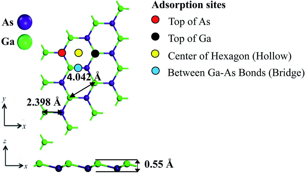


 . Here, A is a proportionality constant, Eg is the band gap of the pristine or gas adsorbed structure, kB is the Boltzmann constant, and T is the temperature. The change of conductivity can thus be used to define sensitivity and can be expressed as


 , where υo is the attempt frequency. Previous reports determined the attempt frequency of NO2 to be 1012 s−1.76 According to previous works, it is reasonable to assume the same attempt frequency for other gas molecules.18,77,78 The considered temperature was 300 K. The recovery times at temperatures 300–600 K are summarized in Table 5.