 Open Access Article
Development of nano- and microdevices for the next generation of biotechnology, wearables and miniaturized instrumentation
Luna R. Gomez Palaciosa and
A. Guillermo Bracamonte *abc
*abc
aInstituto de Investigaciones en Físico Química de Córdoba (INFIQC), Departamento de Química Orgánica, Facultad de Ciencias Químicas, Universidad Nacional de Córdoba (UNC), Ciudad Universitaria, 5000 Córdoba, Argentina. E-mail: gbracamonte@fcq.unc.edu.ar; guillermobrac@yahoo.ca
bDepartment of Chemistry, University of Victoria (UVic), Vancouver Island, V8W 2Y2 British Columbia (BC), Canada
cDépartement de chimie and Centre d'optique, photonique et laser (COPL), Université Laval, Québec (QC), G1V 0A6, Canada
First published on 27th April 2022
Abstract
This is a short communication based on recent high-impact publications related to how various chemical materials and substrate modifications could be tuned for nano- and microdevices, where their application for high point-of-care bioanalysis and further applications in life science is discussed. Hence, they have allowed different high-impact research topics in a variety of fields, from the control of nanoscale to functional microarchitectures embedded in various support materials to obtain a device for a given application or use. Thus, their incorporation in standard instrumentation is shown, as well as in new optical setups to record different classical and non-classical light, signaling, and energy modes at a variety of wavelengths and energy levels. Moreover, the development of miniaturized instrumentation was also contemplated. In order to develop these different levels of technology, the chemistry, physics and engineering of materials were discussed. In this manner, a number of subjects that allowed the design and manufacture of devices could be found. The following could be mentioned by way of example: (i) nanophotonics; (ii) design, synthesis and tuning of advanced nanomaterials; (iii) classical and non-classical light generation within the near field; (iv) microfluidics and nanofluidics; (v) signal waveguiding; (vi) quantum-, nano- and microcircuits; (vii) materials for nano- and microplatforms, and support substrates and their respective modifications for targeted functionalities. Moreover, nano-optics in in-flow devices and chips for biosensing were discussed, and perspectives on biosensing and single molecule detection (SMD) applications. In this perspective, new insights about precision nanomedicine based on genomics and drug delivery systems were obtained, incorporating new advanced diagnosis methods based on lab-on-particles, labs-on-a-chip, gene therapies, implantable devices, portable miniaturized instrumentation, single molecule detection for biophotonics, and neurophotonics. In this manner, this communication intends to highlight recent reports and developments of nano- and microdevices and further approaches towards the incorporation of developments in nanophotonics and biophotonics in the design of new materials based on different strategies and enhanced techniques and methods. Recent proofs of concept are discussed that could allow new substrates for device manufacturing. Thus, physical phenomena and materials chemistry with accurate control within the nanoscale were introduced into the discussion. In this manner, new potential sources of ideas and strategies for the next generation of technology in many research and development fields are showcased.
1. Introduction
The design and manufacturing of devices is today a high-impact research field with consequent impact on other multidisciplinary fields, as well as on the market of chips,1 nano- and microfluidics technology2,3 and wearables.4 To reach the current level of technology it has undergone a long process of development and knowledge creation based on fundamental research.In this perspective, this review communication intends to discuss recent reports directly related to a variety of device approaches toward new ones that could be generated incorporating different physical phenomena and materials chemistry strategies, where the control of the nanoscale has shown a high impact on the material used for devices. In this context, several designs for devices, waveguides and wearables for the detection of different targeted biochemical species have been proposed. The signaling recorded in the different developments was different, and has shown varied detection levels and resolution. Many of them operated through the generation of non-classical light,5 light scattering,6 electronic conduction,7 and bioimaging.8
The study and application of signal transduction through modified substrates depended on the targeted chemical species. Similarly, the incorporated optical set up was taken into account and in many cases adapted to accomplish the desired function. The use of light emitting devices (LEDs),9 organic light emitting devices (O-LEDs),10 wireless approaches11 and miniaturized instrumentation12 showed their impact on studies at this level. Moreover, the use of nanoparticles and nanoplatforms proved their use as nano-tools for lab-on-particles,13 smart responsive optical nanomaterials, and nano-biolabellers for bioimaging and biodetection (Fig. 1).14
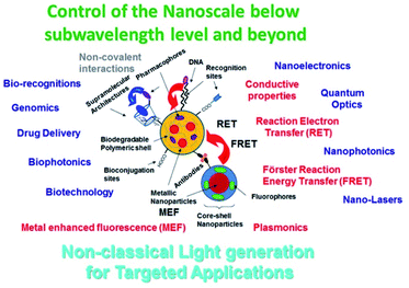 | ||
| Fig. 1 Scheme of tuneable properties based on variable nanoarchitecture for targeted applications (blue). Type of nanoparticles, chemical modification and physical properties developed (black). Reproduced from ref. 13 with permissions of Bentham Science Publishers, Copyright 2021. | ||
Therefore, this review allowed discussion of enhancements strategies of non-classical light and electronic conductions. Metal-enhanced fluorescence (MEF),15 fluorescence resonance energy transfer (FRET),16 enhanced FRET,17 and coupled MEF-FRET18 phenomena were discussed. In a similar manner, enhanced conduction by high electromagnetic fields interactions from several plasmonic sources were also considered.19 Moreover, enhanced plasmonics (EP)20 studies and approaches were introduced to bioapplications and assays. Studies of these phenomena are currently in progress from single nanoplatforms developments. In many cases this has led to the discussion of their incorporation in new devices through substrate modification or being used as nano-tools to transduce signals from confined spaces and volumes in nano- and microfluidics designs.
In the generation of enhanced non-classical light emission from light–matter interactions, silicon Raman laser21 developments as well as related enhanced light scattering22 should be taken into account. Various optical approaches have been reported in this research field, such as the use of modified silica substrates, surfaces, waveguides, optical resonators and other setups, which contribute to the design of functional devices.23 In this context it could be noted for example how the control of nanochemistry has allowed to modify light scattering properties. The capability to organize hybrid silica NPs towards hybrid silica nanoarrays could lead to modified surfaces and substrates for improved light scattering resonances and increased signaling from the surface, across and through the materials by means of different approaches such as photonics surfaces, materials and waveguide substrates respectively.24 In this manner, it would be possible to tune new properties in various optical substrates for new device designs of variable sizes and geometries.
This knowledge construction made it possible to discuss in particular the detection of low-level concentrations such as single molecule detection (SMD),25 biomolecules, biostructures, and other applications such as drug and light delivery, and opto-stimulation26 (Fig. 2). The focus was on developments in life sciences by the discussion of developments already reported in previous communications. However, the discussion highlighted the incorporation of new nanotechnology proofs of concept such as smart optical transducers for future device developments. In addition, new approaches were considered where devices could be coupled with advanced optical instrumentation after use, as well as the incorporation of portable and miniaturized instrumentation. In this way, new insights and strategies were proposed that could be applied in the future with potential use in the development of enhanced functionalities and improved nano- and microdevices for the next generation of biotechnology, wearables and miniaturized instrumentation.
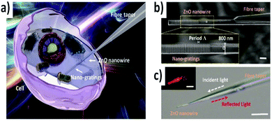 | ||
| Fig. 2 Schematic illustration and design of the fiber nanogratings sensor: (a) schematic diagram of the ZnO nanogratings integrated on a fiber bioprobe; (b) SEM image of the fiber sensor, with a nanowire diameter of 800 nm. Scale bar, 1 μm. Inset, details of the nanogratings in the yellow dashed rectangle; (c) microscope image of the fiber sensor with the nanogratings against a bright field. Scale bar, 10 μm. Inset, microscope image of the nanowire against a dark field, with incident light of 633 nm. Scale bar, 5 μm. Reproduced from ref. 26 with permissions of Advanced Photonics, Copyright 2022. | ||
2. Concepts from the nano- and microstructure design to the functional substrate and targeted device
In the design of nano- and microdevices, control of matter and its properties is required to develop targeted properties. In this sense, chemical control of atoms in molecular structures has made it possible to obtain variable controlled sizes below the nanometer, whereas by applying the appropriate structures and conditions it was possible to develop higher sized materials such as films, and solid substrates such as plastics, porous materials, gels, crystals, etc.27 Moreover, by the control of media in colloidal dispersions a variety of nanostructures were obtained, formed by different atoms and molecules that could provide the desired properties for a given application.28 In this manner, the control of particle dimensions with different shapes in the nano- and microscale could be used as a platform for chemical modifications and functionalization. Moreover, it should be highlighted that in addition to the use of wet chemical methods of synthesis,29 laser-assisted techniques could be applied to modify surfaces and obtain nanostructures as well.30 Thus, accurate dimensions, sizes and shapes could be available to tune properties. These properties could be related to different phenomena such as electronic conductions,31 quantum phenomena,32 non-classical light generation,33 catalysis,34 electromagnetic fields,35 luminescence,36 energy transfer,37 energy storage,38 signal amplification,39 signal transduction,40,41 etc. (Fig. 3).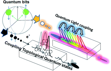 | ||
| Fig. 3 Schematic concept of a modified substrate for targeted electronic, quantum, and non-classical light signaling. Reproduced from ref. 40 and 41 with permissions of Current Material Science (CMS), Bentham Publishers, Copyright 2021. | ||
Based on these properties that could be tuned within confined dimensions depending on material constitution, prototypes for lab-on-particles, nano- and micro-devices with targeted functions could be developed.42 The functions mentioned could be related to a variety of particular needs such as cell, unicellular micro-organisms, and bacteria detection by bioimaging, and drug and non-classical light delivery. Therefore, it is required that functional devices act as smart responsive materials by controlled stimulation. For example, the manufacturing of confined bi-colored laser dyes within silica nanoparticles could switch variable light emissions and intensities depending on the excitation applied and particular objectives such as imaging and targeted light delivery in the surrounding area (Fig. 4).43
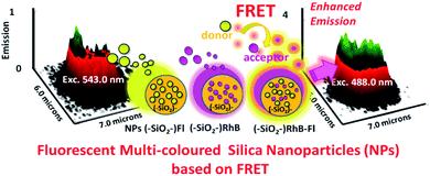 | ||
| Fig. 4 3D fluorescence surfaces from multi-colored SiO2–RhB–Fl nanoparticles with only optimal excitation of RhB as a fluorescent energy acceptor at 543 nm and only optimal excitation of Fl as a fluorescent energy donor at 488 nm and coupling with RhB as a fluorescent energy acceptor. Inset images show the laser dyes incorporated within the silica nanoplatforms. Reproduced from ref. 43 with permissions of Journal of Nanophotonics, SPIE, Copyright 2020. | ||
In this manner, a number of functions could be developed related to different applications by nanophotonics,44 classical and non-classical light generation within the near field, microfluidics and nanofluidics, signal waveguiding,45 quantum-, nano- and microcircuits,46 smart responsive stimulation of functions as functional switcher,47 etc. (Fig. 5).
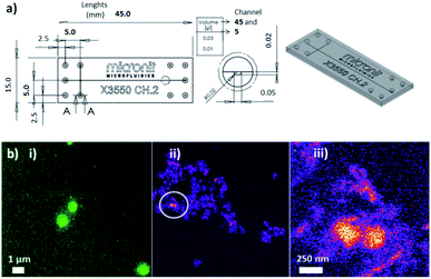 | ||
| Fig. 5 (a) Scheme of cross channel microfluidic chip. (b) Inset images correspond to (i) ultraluminescent gold core–shell silica NPs and (ii) and (iii) modified silica nanoparticles with supramolecular systems as mimetics of antibody–antigen interactions for targeted organic fluorescent molecular reporter complexations and detection by laser fluorescence microscopy. Reproduced from ref. 45 with permissions of Micronit Microfluidics Company, and Frontiers in Drug, Chemistry and Clinical Research, OAText, Copyright 2019. | ||
The desired applications in life sciences technology are varied, such as imaging,48 diagnosis, telemedicine,49 portable bioassays,50 single molecule detection (SMD),51 drug delivery,52 in vivo monitoring, remote monitoring, and portable and wearable devices for real-time monitoring53 (Fig. 6).
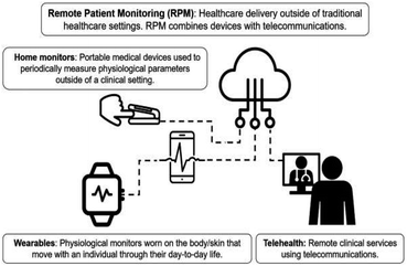 | ||
| Fig. 6 Wearables, home monitoring technologies, and telehealth combine to provide the framework for RPM. There has been a substantial increase in the implementation of telehealth and RPM technologies during the COVID-19 pandemic. There have also been regulatory changes to encourage further adoption of RPM technologies during the pandemic. This figure contains visual elements that are licensed under CC BY. Reproduced from ref. 49 with permissions of Journal of Biomedical Optics, SPIE, Copyright 2020. | ||
For all these reason, the literature under review highlights the importance of chemical synthesis control applied to the design of new materials in the nano- and microscales in order to obtain substrates or macroscopic materials whose shapes and properties could be tuned. Therefore, a micrometer- or millimeter-sized substrate with a given function could be obtained based on the several components.
In this way, it should be highlighted that this bottom-up opened new opportunities for research as well as offering new strategies for other research fields such as nanophotonics, biophotonics, neurophotonics and nanomedicine. In addition, it has already been released in the market as wearable consumables.54
3. Current trends and future perspectives of implantable, portable and wearable devices and chips in biology and medicine
This section deals with the detection of biomolecules and its potential uses in biology and medicine, based on the nano- and microstructures designed. These structures, based on the use of different chemical synthesis processes, allowed to modify surfaces to tune targeted signaling. Thus, it was considered how smart responsive nano- and microplatforms made possible free targeted interactions in colloidal dispersions, incorporated in nanofluidics and microfluidics as well as in advanced standard in-flow cytometry instruments available in the market. In addition, the use of the platforms mentioned of variable sizes and material compositions on modified substrates for device and chips designs was highlighted. These modified substrates could be excited by a number of sources of radiation depending on the targeted physical signaling, wavelength, or mode of energy. This enabled the detection of molecules at very low concentrations within levels of single molecule detection (SMD). These phenomena could be developed in different optical setups and approaches, which could open new strategies for e.g. drug research, or chemical and clinical research.55These devices and chips could be used in other studies and applications such as in-flow nanoplatforms, various biostructures, cells detection, and tracking within cells and organelles. Thus, many research projects are currently in progress, as well as a number of developments in nanophotonics,56,57 biophotonics,58,59 genomics,60 next-generation sequencing techniques,61 neurophotonics62 and nanomedicine63 (Fig. 7).
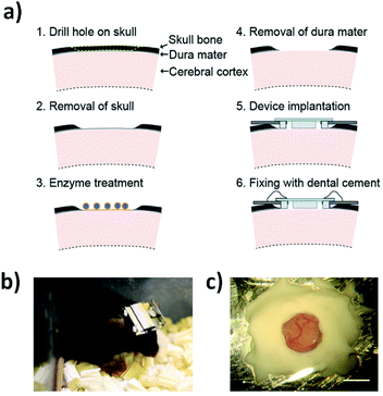 | ||
| Fig. 7 Lab-on-a-brain: implantable micro-optical fluidic devices for neural cell analysis in vivo. Device implantation procedure and a mouse implanted with the device: (a) Low invasive device implantation procedure with dura removal using enzymatic treatment; (b) photograph of a living mouse with the headgear attached on its head. The micro-optical fluidic device was protected by placing it inside metal headgear with a detachable cover; (c) close-up photograph of the implanted device after fixing it mechanically with dental cement. Scale bar, 2 mm. The schematic illustration was drawn by H. T. using Adobe Illustrator software, and the photographs were taken by A. N. Reproduced from ref. 62 with permissions of Scientific Reports, Springer Nature, Copyright 2014. | ||
Moreover, thanks to the possibility of incorporating them in vivo, depending on the design used, real-time tracking was implemented by the development of wearables64 and portable devices. In the same way, the development of miniaturized instrumentation is noteworthy, such as miniaturized endoscopes,65 microscopes,66 and optrodes67 for in vivo applications and portable uses as well. Some of the highlights are portable microscopy on rat skulls for neurophotonics, endoscopy on living tissues with improved imaging to detect molecular modifications in tissues during cancer development, and optrodes with direct variable signaling tracking in place depending on the requirements. Similarly, a notable level of miniaturization and power of analysis has been achieved by using microscopy setups of reduced sizes, by fine-tuning minimal-sized optical lenses in a confined cylindrical volume with a diameter of few mm. This capability has enabled the development of an open-source, wireless miniaturized microscope system to track in vivo calcium ion delivery from neurons by incorporating a specific fluorescence probe.68 The optical setup led to single-photon fluorescence imaging in freely behaving animals. The device was made by 3D printing and weighted only 1.8 g. In this manner, it was possible to image different fluorophores as calcium ion indicators. The power of analysis recorded by wireless imaging to generate high-quality and acceptable analytical performances for quantifications should also be highlighted.
In addition, the implementation of the nano- and micro-platforms mentioned above on devices and chips, allowed to develop new approaches for precision medicine. In this high-impact point-of-care research area the use of lab-on-particles, cargo-particles, gene detection, and new drug delivery systems are greatly needed. Thus, the nanochemistry and chemistry of materials accompanied by the appropriate incorporation of technology such as optical platforms, support substrates, lasers, photon and quantum sources, and detectors could make possible to prototype new designs for other uses and applications.
On this topic, focused on the importance of nano-optics for targeted biosignals in tissues and real samples, the development of implantable photonic neural probes for light-sheet fluorescence brain imaging has recently been reported.69 This imaging approach was successfully achieved by the use of a miniaturized optical setup along with the incorporation of a probe with a propagation capability of distances up to 300 μm in free space using fluorescent optical responsive beads suspended in agarose as medium. The different steps involved in the design and several lithography and surface modification techniques should also be mentioned. Neural probes were manufactured on 200 mm-diameter Si wafers. A 135 nm-thick SiO2 bottom cladding and SiN waveguide layer were deposited by plasma-enhanced chemical vapor deposition (PECVD); and fully etched SiN waveguides were formed using deep ultraviolet (DUV) lithography followed by reactive-ion etching (RIE), and the 1.55 μm-thick PECVD SiO2 top cladding layer was then deposited. Moreover, knowledge of wet chemistry techniques and methods was applied to set the adequate optics of beads as well to other examples previously discussed. This demonstrated the importance of a multidisciplinary approach that can bring together different fields and technologies such as wet-chemical methods70 and laser-assisted techniques,71 which allow variable chemical matter compositions for alternative strategies in the design of nano- and microdevices.
Thus, the importance of chemistry, physics, optics, and material science to control the nanoscale and further to develop new functionalized materials was shown; however, it was the multidisciplinary approach that made the previous developments and applications possible, by combining different sources of knowledge. This is just to obtain the platform, functional substrate, or device, which in turn could later open new pathways for study, research and analysis. It was the intent of this study to review the state of the art in these fields, accompanied by building the knowledge from the molecular level to the macroscopic or miniaturized instrumentation design.
4. Insights into nano-optics for in-flow devices and chips for biosensing
In order to design and synthesize various highly responsive materials for devices and chips, the importance of material tuning and control at the atomic level in 3D to quantum and nanoscale sizes should be noted. This led to lithography techniques as well such as wet-chemistry methods to manage colloidal dispersions. Thus, looking for biosensing applications, nanotechnology and biotechnology made possible the development of different optical properties with potential uses for device and chip designs. In this perspective, fundamental and applied nano-optics is of the utmost interest, particularly the design and manufacturing of silica waveguides, organic, and hybrid substrates for signal translations through the material. Therefore, resonant plasmonics waveguides for enhanced performances are currently being developed. Thus, metal-enhanced fluorescence in plasmonic waveguides has been reported, developing an accurate control of plasmonic nanoparticles to manufacture plasmonic waveguides via self-assembly into linear structures with very small inter-particle separation.72 Wrinkled PDMS stamps were used to obtain large micrometers of length of one-dimensional nanoparticle assemblies. Combining this technique with the use of tunable, metal–dielectric, core–shell nanoparticles allowed the manufacturing of linear assemblies with adjustable inter-particle separation for improved performance of non-classical light translations through the modified substrate. In a similar manner, by combining other semiconductive materials using lithography techniques photonic-crystals could be tuned as electro-optic modulators,73 which allowed tuning of photon delivery within the nanoscale on chips (Fig. 8).74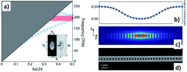 | ||
| Fig. 8 Design of LN photonic crystal nanocavity. (a) Dispersion property of the designed LN photonic crystal nanobeam for the TE-like polarization. The inset shows the structure of the unit cell (top view). The red point indicates the frequency of the fundamental TE-like point-defect mode, and the colored pink region indicates the photonic bandgap. (b) Lattice constant as a function of position, which is optimized for high radiation-limited optical Q. (c) The optical mode field profile of the fundamental TE-like cavity mode simulated by the finite element method. The left inset shows the orientation of the LN crystal where the optical axis is along the z direction. (d) Scanning electron microscopic image of a fabricated LN photonic crystal nanobeam. Reproduced from ref. 74 with permissions of Optica, OSA, Copyright 2019. | ||
These highly sensitive substrates based on different light and electronic pathways are examples of how the control of nano-optics allows signal translation in space and time. These signals could be related to various recognition events where signal modification is required. Therefore, the analysis of single nanoplatforms is also of interest toward collective interactions of higher-sized materials in the micrometer scale with close-proximity targeted devices in the macroscale. Thus, highly sensitive responses from single nanoplatforms could be coupled and transduced through various substrates in waveguides as well as being part of smart nanoparticles accurately placed in in-flow devices and chips. In this perspective, the importance from microfluidics to nanofluidics, and signal wave-guiding by controlling sizes and nanostructured materials for nanophotonics, biophotonic resolution, and drug delivery, should be highlighted as well.75 So, depending on the targeted application, optical properties and materials could also be tuned. In this regard, there are many recent developments focused on single nanoparticle spectroscopy, and analysis with potential applications in SMD, biosensing, and biophotonics.
In this context the importance of molecular control at the nanoscale as well as in the quantum scale should be noted, due to their close proximity to molecular dimensions. Therefore, the challenge is to recognize the arrival of targeted molecules on nanopatterned surfaces or single nano- or quantum platforms. In this manner, SMD approaches could be feasible in the next generation of substrates for devices, wearables and implantable chips with perspectives of biodetection at low concentration levels. These approaches could eventually combine depending of the demand for diagnoses and treatments with permanent and non-permanent optical detection systems. This opens the possibility of variable combinations. However, the device substrate or material should be highly smart and sensitive in their close surrounding. In this context, various physical phenomena should be mentioned related to electronic oscillations and the generation of high-energy electromagnetic fields such as plasmonics76,77 as well as other electronic phenomena. These could affect their near environment within short nanoscale lengths known as the near field. For example, metal-enhanced fluorescence (MEF) is a plasmonic phenomenon in the near field where the fluorophores are excited by the electromagnetic field from the electronic oscillation of the metallic surface. In this manner, a higher electronic occupancy is produced in the excited state accompanied by enhanced radiative decay and fluorescence lifetime shortening, which produce an increase in the luminescence from the fluorophores close to the metallic surface within the near field.78 In this way new analytical methodologies and biotechnological applications were proposed and are in progress,79–81 shaping the future of the next generation of nanotechnologies.82,83 In addition, the level of control achieved by the new trends mentioned in nanotechnology should be highlighted, for example by the control of optical properties based on plasmonics surfaces, re-shaping intensity distributions by laser excitation. Thus, a reversible shape and plasmon tuning in hollow AgAu nanorods was developed, with generation of spatially controlled high electromagnetic fields by laser excitation.84 This capability to control nanomaterial and properties could lead to switchable functions, spatially controlled electronic conductions, and highly sensitive surface emitters for smart photonics surfaces in new devices, chips and wearables.
In addition, other phenomena such as fluorescence resonance energy transfer (FRET) could be modified by the presence of metallic surfaces. In this regard, the effects of metallic silver particles on FRET between fluorophores bound to DNA have been studied.85 This research work, as well as others carried out by recognized researchers in this field, have allowed improved FRET between the energy donor–acceptor pairs placed at a controlled distance from the plasmonic surface. Moreover, recent scientific communications highlight the development of multilayered silica core–shell nanoplatforms86 applied to label-free biosensing of DNA based on multilayer fluorescent nanocomposites and a cationic polymeric transducer.87 This approach has led to the detection of some targeted DNA strands on nanoparticles and nanoaggregates by coupling the increased fluorescence of a polymeric transducer intercalated in complementary DNA strands with a metal-enhanced fluorescence shell placed at an optimal distance from the plasmonic core. Therefore, the fluorescence energy was transferred by FRET and coupled with the MEF receptor rising to an augmented sensitivity only in the presence of the complementary DNA strand. Therefore, the energy emitted by the energy donor was absorbed by an enhanced energy acceptor that allowed amplified signaling through the nanomaterial for DNA detection. In this manner, direct molecular detection of SRY gene from unamplified genomic DNA by MEF and FRET coupling was achieved.88 In this approach the complex biomachinery involved in the augmentation of genomic material in traditional techniques was replaced by an enhanced nano-optical approach. In this perspective the new substrates for the next generation of devices could provide improved performances for early diagnosis and detection where SMD will be required. Moreover, the fundamental issue of biocompatible properties should be contemplated. In this perspective inert and non-toxic materials should be evaluated along with the desired highly sensitive nano-optics. For this reason, the effect of the plasmonic properties of gold on enhanced luminescence based on MEF was studied by the application of biocompatible gold citrate nanoparticles modified with silica spacer and covered with a fluorescent shell with the incorporation of a conjugated laser organic dye. This led to ultraluminiscent gold core–shell nanoparticles as nanoimaging platforms for biosensing applications based on MEF.89 These nanoparticles were developed and optimized to exhibit the maximal response from collective single nanoplatforms; however, there is still need of SMD applications. In this regard, in-flow nano-optics studies from near-to far field detection based on MEF signaling were later reported (Fig. 9).90 In this research, the optimal properties for MEF signaling from single nanoplatforms excited by laser application in in-flow colloidal dispersions were studied. Thus, drastic signal modifications were achieved, depending on the main MEF parameters such as spacer length from the gold core, concentration of laser dyes incorporated, and excitations applied. These preliminary results showed potential transference to smart responsive single nanoplatforms as well as nano- and micro-arrays, from where molecular signaling could be collected at various levels of concentration.
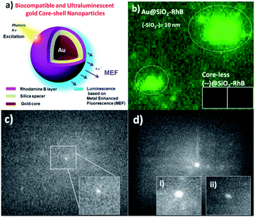 | ||
| Fig. 9 (a) Schema of ultraluminescent gold core–shell nanoparticles based on metal enhanced fluorescence (MEF) (Au@SiO2–RhB NPs); (b) nano-imaging of Au@SiO2–RhB NPs by laser fluorescence microscopy. Inset image corresponds to core-less NPs; (c) in-flow nano-imaging by IFC of single ultraluminescent Au@SiO2–RhB NPs (sample s2 with SiO2 = 10–11 nm). Inset image corresponds to sizes of 100–200 nm; (d) higher sized ultraluminescent Au@SiO2–RhB NPs in concentrated conditions. Inset images (i) and (ii) correspond to core–shell and core-less nanoparticles after application of the sodium cyanide methodology respectively. Reproduced (a) and (b) from ref. 89; and (c) and (d) from ref. 90 with permissions of RSC Advances, Copyright 2017, and Microchemical J., Copyright 2021 respectively. | ||
Moreover, these ultraluminescent properties were transferred to biomembranes of Escherichia coli bacteria which allowed to generate synthetic ultraluminescent bioimaging with stable signaling from individual bacteria detection based on MEF nanoimaging.91 In a similar manner, these achievements showed potential applications in nano-bio-optics for detection of virus and higher-sized biostructures as well.92 These developments and the required optical setups could be proposed within portable devices and miniaturized instrumentation. In this regard, in-flow MEF biolabelling and biodetection of Escherichia coli bacteria have been reported recently.93 This study described improved performances of biostructure detection in continuous in-flow movement by applying ultraluminescent nano-biolabelling. This led to the characterization of different distributions of labelled and non-labelled biostructures, as well as free nano-labellers. It should also be noted that the proposed nano-biolabelling was based on non-covalent interactions, thus obtaining improved performances by application of targeted antibody–antigen approaches or related strategies. So, the capability to manage non-classical light from confined nano-emitters leading to bioimaging could be incorporated in imaging-based devices that could be resolved with portable instrumentation and even incorporated with smart telephones, which would provide accessibility to users.94
In this context, other proofs of concept and targeted developments focusing on SMD levels of labelled and free labelling approaches could be mentioned from recent reports. For example, the use of synthetic molecular receptors such as cyclodextrins attached to gold nanoparticles allowed improved laser dyes detection based on enhanced plasmonic effects.95 This research work showed how modifications to the medium could control from single grafted nanoparticle detection to higher-sized nanoaggregates, with potential uses for photonic surface applications. But the importance of the potential use of single nanoplatforms to design lab-on-particles should be highlighted as well, where biodetection and targeted application of treatments could be combined if required by smart responsive stimulus.96 For example, the design and synthesis of hybrid silica substrates and nanoparticles of variable sizes could be easily managed to tune signal conduction by varying electronic properties, energy modes, and photonics signaling through the modified material. Moreover, the signal generated could be translated to longer distances, and coupled with other types of materials; by way of example, synthetic non-classical luminescence coupling from silica nanoplatforms to unicellular micro-organism with a consequent generation of enhanced nano-bio-FRET luminescence could be mentioned (Fig. 10).97
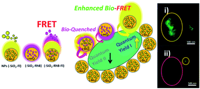 | ||
| Fig. 10 A schematic diagram showing the biolabelling of cyanobacteria (cysbact) with fluorescent mono-colored SiO2–Fl and SiO2–RhB NPs and multi-colored SiO2–RhB–Fl NPs, by non-covalent interactions. Inset image: (i) and (ii) fluorescence laser microscopy bioimaging of labelled cyanobacteria with SiO2–Fl, and SiO2–RhB respectively. Reproduced from ref. 97 with permissions of RSC Advances, Copyright 2021. | ||
The effect mentioned was controlled by the incorporation of the proper laser dye emitters in silica nanoparticles and targeted laser excitation to light delivery and transference through the biomaterial. In this perspective, the proposed generation of new free labelling bioimaging approaches from modified substrates could also be mentioned.
Another mode of energy generated by optical excitation of modified substrates that should be noted is light scattering from a large spectrum of matter sources and chemical compositions. This phenomenon is particularly studied and generated from silicon-based substrates and modified surfaces to cause phenomena such as silicon lasers (SL) and surface enhanced Raman scattering (SERS).98
For beginners, a laser is a device that emits high-energy light produced by optical amplification based on stimulated emission of electromagnetic radiation.99 Laser light should be coherent, a property which is related to an ideal state of waves enabling stationary (i.e. temporally and spatially constant) interferences. These characteristics are not easy to create and depend on many factors such as materials and optical setup. In this context, to achieve an optical gain or lasing from silicon is a permanent challenge, because this material in bulk shows semiconductor bandgaps and very low light emission efficiency. In this regard, there are many interesting reports and other research currently in progress based on optical resonators with varied sizes and designs,100 such as heterostructures with incorporation of nanocavities that have led to silicon Raman laser signaling.101 The radius of the nanohole was 128 nm, with spacers at various intervals within 400–420 nm. This configuration allowed the propagation of two energy modes, Stokes and Pumped. Thus, the polarization of the direction of the light was orthogonal to the x–y plane in this geometry. In this manner an integrated optical circuit was developed by using a (100) SOI wafer with a 45 degree-rotated top silicon layer for improved efficiency.
These types of developments are of great interest, due to their versatility and tuneability, coupled with several other physical properties, from the small organic molecular level102 to nano-plasmonic modifications103 which lead to new properties and applications, e.g. in SERS approaches.104
In addition to targeted functionalities from molecules to the nanoscale and beyond, the importance of the support material or substrate should be mentioned as well as its particular properties depending on the phenomena under study. Thus, in addition to many silica or silanized examples, other types of polymers such as stretchable polymeric materials based on various organic monomers and hybrid materials.105 In this way, a large variety of skin implantable devices could be mentioned, such as the development of expandable and implantable bioelectronic systems for analyzing and regulating real-time activity of the urinary bladder (Fig. 11).106 This research work presented a stretchable wearable that allowed to sense length stretching of bladder, accompanied with optical sensing and light delivery for targeted optogenetics.
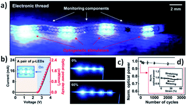 | ||
| Fig. 11 Electrical and optical properties of the devices in the E-thread. (a) An optical image of the E-thread, built with eight μ-LEDs distributed onto four islands and three monitoring components [strain gauge, electromyography (EMG) electrodes, and temperature meter]. (b) Electrical and optical characteristics of a pair of μ-LEDs, with the optical image in the inset. (c) Photographs of the E-thread before (top) and after applying strain up to 60% (bottom). (d) Normalized light intensity as a cyclic extension of the E-thread up to 60% (n = 5). Reproduced from ref. 106 with permissions of Sci. Adv., Science, Copyright 2020. | ||
Anothers development that could be presented concerns skin-mounted soft electronics with a number of applications, such as signal transductions and decoding, depending on the functionality. Thus, mechano-acoustic signaling as recorded by the stethoscope was recorded by an implantable wireless device at the suprasternal notch.107 In this manner acoustic signals were obtained from subtle vibrations of the skin at accelerations of around 10−3 ms−2 to large motions of the entire body at about 10 ms−2 and frequencies up to around 800 Hz. This high sensitivity was applied to other phenomena produced in the body such as daily activities and exercise, with real-time recordings of heart rate, respiration rate, energy intensity, other essential vital signs, and other unconventional biomarkers as well. And in connection with this the development of an automated, multi-parametric monitoring of respiratory biomarkers and vital signs in clinical and home settings for COVID-19 patients should be particularly highlighted.108 This device was also based on mechano-acoustics signatures from core, respiratory vital signs recording, and expressed biomarkers such as coughing count.
Therefore, as could be seen in the previous examples, the materials used for a given targeted application were responsible for energy translations related to mechano-acoustics signals. But the concept was also developed for other associated signals and wavelengths where the required tuning of the properties of new materials and metamaterials should be noted.109 In this regard, the design and synthesis of metalenses of reduced sizes for imaging applications could be mentioned.110 Metalenses are an array of optical nanoantennas on a surface capable of manipulating the properties of incoming light. Several functionalities were tuned based on this approach by the incorporation of flat optical components such as polarizers, optical imaging encoders, tunable phase modulators and retroreflectors. Thus, in the research work mentioned above achromatic aberrations were eliminated, which allowed full color imaging within a large interval of wavelengths. Moreover, the control of matter such as photonic crystals could be assembled and controlled by chemical surface modifications leading to varied absorption and emission wavelengths. These properties could be transferred through space and time for targeted applications as well.111 Thus, plasmonic tuning of optical fibers was reported for biosensing,112 and in particular the recent development for optical virus detection of SARS-CoV-2/COVID-19 can be highlighted.113 This shows the importance of material constitution and high sensitivity against surface modifications of reduced-size devices and chips. Thus, just in this case potential transference to wearables and implantable biosensing technology could be evaluated.
5. Perspectives towards biosensing and single molecule detection (SMD) applications
The development of chips, wearables and device implants is of great interest for many applications; however, their uses could be particularly targeted to bioapplications, clinical analysis and medical diagnosis. Due to its versatile and practical point of view based on data collected in vivo, in continuous real-time monitoring, it has a high impact on approaches and studies focused on the determination of various biomolecules, metabolites, and analytes within low concentration intervals. In this regard, it is well known that single molecule detection (SMD) provides the best known level of detection of various molecules by the application of several chemical, physical and optical strategies. In this context, this section discussed potential applications in SMD, developing different strategies. Moreover, it should be mentioned that the examples discussed allowed different approaches that have potential implications in this research field. It is known that the optics required for SMD developments is not as simple as to be carried on implantables; however, chips, devices and implantables could be designed and sensed as required by proper optical systems. In this way, a chip could be designed to act as a molecular trap during a certain number of hours, and then detect low numbers of molecules within confined spaces in the nano- and microscale.In this perspective, there is actually a huge advance from companies that offer wearables for health monitoring tracked by smart phones on demand.114 Promising results are offered for early diagnosis and treatment. On the other hand, fundamental research is showing advances in several materials for highly sensitive detection with low concentration levels. For example, optical writing and single-molecule reading of photoactivatable and silver nanoparticle enhanced fluorescence could be mentioned.115 In this approach a hybrid nanoparticle-molecular system was developed, formed by silver nanoparticles and a fluorogenic boron dipyrromethene (BODIPY) that is selectively activated by UVA or UVC light in the presence of a targeted photoacid generator. In this manner accurate single-molecule readings were achieved in the near surrounding of the plasmonic structure. These types of developments placed in confined spaces accompanied by a proper tuning could lead to chips and devices coupled with different advanced microscopy optics and techniques. In addition, the possibility to add complementary functions such as drug delivery or patches as wearables could provide on site solutions to various health problems. The recent report about the first 3D printing of wearable personalized oral delivery devices applied to humans could be mentioned.116 In this approach it was highlighted how a direct translation of materials could be developed for the next generation of drug delivery systems for personalized therapy. These types of devices could be used early if the health problem is diagnosed in advance. This concept could be applied to molecules, biomolecules and biomarkers, as well as biostructures. With this approach, applications from translational medicine and clinical diagnosis to biodetection could also be developed.117 In this way, optical resonators, nanocrystals, plasmonic structures, nanopatterned surfaces and waveguides were developed as smart responsive substrates with potentials applications in portable devices, chips, and new wearables. However, it should be noted that simple paper-based chips based on solid optical responsive substrates as well as within microfluidics approaches could be considered. For example, the detection of trace levels of chemical and biological analytes has many important applications, including forensics and environmental monitoring which were achieved by surface-enhanced Raman scattering (SERS).118 Thus, the concept was extended on plasmonic paper for trace detection of analytes.119 This approach was based on shape-controlled nanostructures such as gold nanorods, which offered easy tunability of the localized surface plasmon resonance (LSPR) wavelengths from collective electron oscillations occurring in these structures on the modified material surfaces. In this manner, trace quantities of TNT were detected in a chemically complex medium such as shampoo solution, with a detection limit of ∼100 pM. But other bioapplications were also developed for viruses and higher-sized biostructures such as bacteria and micro-organisms. So, versatile and low-cost approaches were developed based on low-cost substrate combined with the proper responsive nanomaterial for targeted signaling.
Similarly, a large quantity of research developments that incorporate immunochemistry for targeted biomolecules and biostructure detection should be mentioned. For example, it was noted that stable silver plasmonic resonant nanoparticles with non-bleaching multicolor optical immunolabels properties led to single targeted molecular detection.120 Moreover, the observation of in-flow devices such as microfluidics could allow immunoassays of cells and tumors by confined, controlled and reduced-size channels and chambers for targeted applications such 3D microfluidic ex vivo culture of organotypic tumor spheroids to model immune checkpoint blockade.121 In this context, the capability to design accurately nano- and microfluidics channels, chambers, and a number of fluidic inlets could provide high-impact insights into implantable device designs such as functional micro-machines covered with specific polymeric materials to avoid undesired reactions (Fig. 12).122
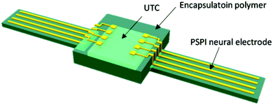 | ||
| Fig. 12 Conceptual drawing of chip-scale biocompatible package. Reproduced from ref. 122 with permissions of Micromachines, MDPI, Copyright 2021. | ||
All these strategies and approaches could be considered as tools for the design of new proofs of concept in the next generation of wearables. In this context, other developments such as lab-on-particles123 for optical biodetection, lab-on-a-disc assays for protein detection by optomagnetic readouts and optical imaging using nano- and microsized magnetic beads,124 and microelectromagnetic traps for DNA detection;125 could lead to new designs of portable and implantable device designs. In this perspective a pilot study was carried out with 20 subjects who underwent physical exercise, where plasma samples were tracked before and 1 h after the workout by extracellular vesicle (EV) detection. These biostructures and their proteome in human plasma provide a novel approach in clinical diagnostics, since they could reflect normal physiological and pathological states of health. For this study an improved wave coupling by acoustic resonators to increase EV recovery was applied.126 This was a clear example where lab-on-a-chips could be applied, and is related to systems where real-time monitoring is vital to track biological variations within through periods of time.
In a similar manner, all related developments for amplifying signals from a single point of contact as well as signal amplification through the responsive substrate could be incorporated. For example, all types of optical resonators,127 oscillators, light tuning,128 and electroactive materials with single molecule concentrations levels129 are also of interest for the design of new devices.
To conclude, and to discuss potential developments of portable, implantable, and wearable devices, the challenge to overcome should be mentioned and well understood. In this context, the recent Nobel Prize in Chemistry for “the development of super-resolved fluorescence microscopy” should be highlighted, where a controlled optical on/off switch molecular emitter was incorporated for SMD imaging.130 This optimized the number of photons recorded from single molecules at room temperature.131 Other examples based on other signals could be mentioned as well, such as single-molecule laser nanospectroscopy with micro-electron volt energy resolution.132 Therefore, the importance of the future of optics in life sciences and its related technological impact was shown.133
Similarly, but considering other scales to track single-molecular detection events, recent developments of smart and highly sensitive nano-platforms could be highlighted.134 Thus, variable nano-optics platform sizes could target different maximal numbers of molecules per nanostructure depending on their dimensions. These values could be between 100–1000 units per nanoparticle considering reduced sizes within the nanoscale. However, signal transduction from single nanoparticles by arrival of individual targeted molecules on these smart responsive optical nanoplatforms could be limited depending on the detection strategy. But promising results from highly sensitive approaches have led to detection in very low molecular concentrations within nM and femto-M.87,95 The values achieved were also recorded with advanced microscopy setups and with microfluidic systems coupled with imaging detections systems. However, for implantable and wearables such optics levels could constrain portable applications; but this apparent hindrance could be overcome by adding time to collect a higher number of targeted molecules on particles to enhance detection, e.g. by improved O-LEDs, nanolasers, and other miniaturized instrumentation. In addition, if the device developed could be coupled on more sensitive excitation and detection sources, such as microscopy techniques on demand daily, it could be obtained higher power of data recording and additional information. In this perspective, the design of portables and implantable modified devices could be developed controlling the nanoscale on their surfaces enhancing signaling through nano-structured substrate.
6. Future perspectives
From the various communications mentioned and discussed many topics and challenges could be highlighted that show impact on the focused functionality of the device. These mentioned strategies by the control of chemistry within the nanoscale and beyond, coupled with variable optical setups of different dimensions, showed high-impact perspectives by different developments recently reported. However, there are many other non-developed designs based on varied combinations of other materials and coupled optical setups that could be contemplated.In the context of miniaturization of instrumentation, flexible polymeric materials135 combined with well-known quality optical polymeric materials such as organosilanes and modified organosilanes136,137 could add important support to enhanced nano-optics coupled with miniaturized lenses (Fig. 13).
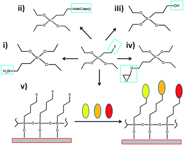 | ||
| Fig. 13 Scheme of chemical versatility of modified organosilanes with different organic groups. Modified tetraethyl orthosilicate (TEOS) with (i) amine groups, (ii) isothiocyanate group, (iii) hydroxyls, (iv) epoxies; and (v) chemical surface modification by the use of modified organosilanes and conjugation with other types of molecules such as optical active structures (represented with colored ovals). Reproduced from ref. 136 with permissions of J. Chem. Res. Adv. (JCRA), Copyright 2021. | ||
Thus, amplified signaling from nanolasers could be added as a source of non-classical light generation for targeted SMD, or light delivery within biostructures. Similarly, the nano-material could be detected thanks to the enhanced non-classical light signaling generated coupled with low power excitation sources with improved detection. These devices and miniaturized instrumentation could show a huge advantage in ease of transportation, portable use, and real-time recording of valuable information. Moreover, the incorporation of wireless and memory could provide remote recording for further analysis, with perspectives in telemedicine, new treatments, and particular needs related to special studies such as variation of metabolites, control of illness, health, and particular physiologies under stress such as ultra-sport performances (Fig. 14).138
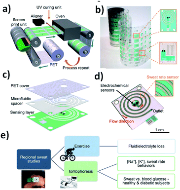 | ||
| Fig. 14 Schematics of R2R fabricated sweat sensing patches for regional and correlative sweat analysis: (a) R2R rotary screen printing of the wearable biosensing patch and (b) optical image of sensing electrode patterns printed via R2R processing are shown. (c) The biosensing patch is assembled by combining the sensing layer, microfluidic adhesive spacer, and PET cover sheet. (d) The assembled biosensing patch includes electrochemical sensors contained within the collection reservoir and electrical sweat rate sensor embedded in the microfluidic channel; (e) the patch, connected to printed circuit board (PCB), can be worn on various parts of the body for regional studies of the composition and dynamics of exercise and iontophoretic sweat. Photo credit: Antti Veijola (VTT) and Hnin Yin Yin Nyein (University of California, Berkeley). Reproduced from ref. 138 with permissions of Science Advances, Copyright 2019. | ||
Moreover, the application of nano- and microfluidics technology incorporated in devices could allow in vivo bio-assays with a single drop of blood or connected in line with the vascular systems of live organisms for controlled drug delivery, depending on need after a biosignal detection. In the same way, other designs for different targeted light and drug delivery uses on site or in the close surrounding could be proposed. The devices could make possible a variety of geometries and surface modifications with potential multifunctional applications. Thus, nano- and micro-syringes for molecular administration provided important insights into portable neurophotonic devices as well as on skin tissues.
So, in future perspectives the device could be regarded as an instrument or tool to be combined with advanced optical setups. And this is where nano-optics and material science could make a valuable contribution.
Finally, it should be mentioned that this section did not intend to follow all the possible directions of future research developments, but was meant to highlight and discuss new combinations of materials and phenomena for future concepts and designs.
7. Concluding remarks
The perspectives discussed in this short review are of a very high impact for drug, chemicals, and life sciences research. But it should be considered not only within these research fields. The same concepts could be incorporated in a similar fashion in other technology developments such for signal waveguiding, nano- and microelectronics, encryption and communications. They are also required for photon, and electron transferences and transductions in devices or miniaturized instrumentation with targeted biological events.Similarly, the capability to control the nanoscale and properties could allow the development of nano-tools that could be incorporated in advanced instrumentation available in the market. In this sense, there are many commercial products such as those related to biological reagents, immune labelled beads, colored beads, bioconjugation reagents, etc. that allow to record more data along with a greater capability for information analysis. From all these developments new applications within biotechnology and nanomedicine using wearable devices are promising new approaches for future technologies in real-time and in vivo analysis.
These advanced approaches related to reduced-size devices showed huge advantages in relation to many aspects of versatility and functionality. The practical point of view of portable uses, added to the capability to detect targeted chemical species or deliver required pharmacophores in real time, could lead to the future development of new treatments. The possible disadvantages are associated with lack of comfort, and the possibility that they are regarded in some cases as an invasive approach. Moreover, perhaps the diminution of sensitivity and resolution depending on the tracked signal, and implicated concentrations, could add additional challenges to overcome by appropriate smart optical responsive material developments, and enhanced optical setup coupling. So, based on the combination of various materials and coupled phenomena to enhance signals and resolutions could be afforded the challenge. Thus, new developments from the quantum-, and nanoscale within the near field to the far field could provide the next generation of functional and smart optical device technology. In this way, it could be mentioned developments about quantum emitters, and ultraluminescent nano-emitters based on enhanced light–matter interactions.139
Then, from the nanoscale to the microscale a number of functional and multifunctional substrates for improved performances could be proposed, depending of the targeted applications.
In these perspectives, this review was intended to discuss new versatile combinations and designs for novel studies of light–matter interactions in life sciences. Thus, the design and manufacturing of devices could lead to future miniaturized instrumentation which is fundamental for the different disciplines of science, and in particular focused on life sciences where real time tracking applications are highly desired.
Author contributions
Luna R. Gomez Palacios contributed with the participation in the Revision of this manuscript as well as with results incorporated and cited in this publication. And, A. Guillermo Bracamonte contributed as Research leader in the context of the Review creation for his recent Research Group formation.Conflicts of interest
There are no conflicts to declare.Acknowledgements
The author gratefully acknowledges the Département de Chimie and Centre d’Optique, Photonique et Laser (COPL), Québec, Canada, for a postdoctoral research position; the National University of Cordoba (Universidad Nacional de Cordoba, UNC), Argentina; and the National Research Council of Argentina (CONICET) for research and teaching positions as well, of A. G. B. Special thanks are due to the Secretary of Science and Technology of UNC (SeCyT), Argentina, for the research grant provided. As well, especially thanks to FONCYT, National Agency of Scientific and Technology promotion of Argentine, PICT A 2020, for the Research proposal acceptation for the Group in formation (Call 2020). Special thanks are also due to Professor Denis Boudreau from COPL at Laval University, Québec, Canada, for allowing the author to participate in his Research project related to genotyping. Thanks as well to Professor Cornelia Bohne for a postdoctoral research position related to Supramolecular Dynamics at University of Victoria, Victoria in Vancouver Island, British Columbia, Canada. Moreover, it is thanks to Professor Burkhard König from the Institut fur Organische Chemie, Universitat Regensburg, Regensburg, Germany, for the Research Visit and Lecture opportunity given in his Laboratory to the author A. G. B. In addition, we acknowledge Professor Nita Sahai from University of Akron, Institute of Polymer Science and Engineering; and NASA Astrobiology Institute, Ohio, United States, for a postdoctoral research position related to the RNA and Origin of Life (OoL) projects. Moreover, we acknowledge recent collaborations in progress in life sciences, with perspectives on single molecule detection (SMD) studies and optical setup developments. So, special thanks are also given to professor Valeria Amé from Centro de Investigaciones en Bioquímica Clínica e Inmunología (CIBICI), Departamento de Bioquímica Clínica, Facultad de Ciencias Químicas (Center of Clin. Biochem. and Immunology Research, Dep. of Clinical Biochem., Faculty of Chem. Sci.) UNC, Argentina. In similar manner, especial thanks to Professor Daniela Quinteros from Unidad de Investigación y Desarrollo en Tecnología Farmacéutica (UNITEFA) (Unit of Research and Development in Pharmaceutical Technology), at Departamento de Ciencias Farmacéuticas, Facultad de Ciencias Químicas (Dept. of Pharmaceutical Sciences, Faculty of Chemical Sci.), from UNC, and her research group. In particular, Ph.D. student Sofia Martinez and researcher Ph.D. Cecilia Tettamanti should be mentioned for their current research work in collaboration related to bioconjugation of nanoparticles. Similarly, it should be acknowledge to Dr Martin Amé, from “Hospital Privado e Instituto Universitario de Ciencias Biomédicas de Córdoba”, Córdoba, Argentine.Notes and references
- G. Alderton, Humans on a chip, Science, 2020, 367(6482), 1087–1088 CrossRef.
- K. Shaw, N. M. Contento, W. Xu and P. W. Bohn, Nanofluidic structures for coupled sensing and remediation of toxins, Proc. SPIE 9107, Smart Biomedical and Physiological Sensor Technology XI, 91070L, 2014, pp. 1–11 Search PubMed.
- M. Pousti, M. Pouyan Zarabadi, M. A. Amirdehi, F. Paqet-Mercier and J. Greener, Microfluidic bioanalytical flow cells for biofilm studies: a Review, Analyst, 2019, 144(1), 68–86 RSC.
- K. San Chun, Y. J. Kang, J. Yoon Lee, M. Nguyen, B. Lee, R. Lee, H. Heul Jo, E. Allen, H. Chen, J. Kim, L. Yu, X. Ni, K. Lee, H. Jeong, J. H. Lee, Y. Park, H. Uk Chung, A. W. Li, P. A. Lio, A. F. Yang, A. B. Fishbein, A. S. Paller, J. A. Rogers and S. Xu, A skin-conformable wireless sensor to objectively quantify symptoms of pruritus, Sci. Adv., 2021, 7, eabf9405 CrossRef PubMed.
- R. Keil, M. Heinrich, F. Dreisow, T. Pertsch, A. Tünnermann, S. Nolte, D. N. Christodoulides and A. Szameit, All-optical routing and switching for threedimensional photonic circuitry, Sci. Rep., 2011, 1(94), 1–27 Search PubMed.
- P. O'Connor and J. Tauc, Light scattering in optical waveguides, Appl. Opt., 1978, 17, 3226–3231 CrossRef PubMed.
- R. Chandrasekar, Z. J. Lapin, A. S. Nichols, R. M. Braun and A. W. Fountain, Photonic integrated circuits for Department of Defense-relevant chemical and biological sensing applications: state-of-the-art and future outlooks, Opt. Eng., 2019, 58(2), 020901 CAS.
- J. Min, L. Ket Chin, J. Oh, C. Landeros, C. Vinegoni, J. Lee, S. Jung Lee, J. Young Park, A.-Q. Liu, C. M. Castro, H. Lee, H. Im and R. Weissleder, CytoPAN—Portable cellular analyses for rapid point-of-care cancer diagnosis, Sci. Transl. Med., 2020, 12, eaaz9746 CrossRef CAS PubMed.
- G. Lozano, S. R. K. Rodriguez, M. A. Verschuuren and J. Gómez Rivas, Metallic nanostructures for efficient LED lighting, Light: Sci. Appl., 2016, 5, 1–10 Search PubMed.
- D. Volz, Review of organic light-emitting diodes with thermally activated delayed fluorescence emitters for energy-efficient sustainable light sources and displays, J. Photonics Energy, 2016, 6(2), 020901 CrossRef.
- S. Q. Wang, T. Chinnasamy, M. A. Lifson, F. Inci and U. Demirici, Flexible substrate based devices for point of care diagnostics, Trends Biotechnol., 2016, 34(11), 909–921 CrossRef CAS PubMed.
- Z. Yang, T. Albrow-Owen, W. Cai and T. Hasan, Miniaturization of optical spectrometers, Science, 2021, 371(6528), eabe0722 CrossRef CAS PubMed.
- A. Guillermo Bracamonte, Frontiers in Nano- and Micro-device Design for Applied Nanophotonics, Biophotonics and Nanomedicine, Bentham Science Publishers, ISBN: 978-1-68108-857-0 (Print); 978-1-68108-856-3 (Online) © 2021 Search PubMed.
- D. Darvill, A. Centeno and F. Xie, Plasmonic fluorescence enhancement by metalnanostructures: shaping the future of bionanotechnology, Phys. Chem. Chem. Phys, 2013, 38, 1–15 Search PubMed.
- C. D. Geddes and J. R. Lakowicz, Editorial. Metal-Enhanced Fluorescence, J. Fluoresc., 2002, 12(2), 1–9 CrossRef.
- H. Dacres, J. Wang, M. M. Dumancic and S. C. Trowell, Experimmental determination of the Forster Distance for two commonly used bioluminescent Resonance Energy Transfer pairs, Anal. Chem., 2010, 82, 432–435 CrossRef CAS PubMed.
- J. Zhang, Y. Fu, M. H. Chowdhury and J. R. Lakowicz, Enhanced Förster Resonance Energy Transfer on Single Metal Particle. 2. Dependence on Donor–Acceptor Separation Distance, Particle Size, and Distance from Metal Surface, J. Phys. Chem. C, 2007, 111(32), 11784–11792 CrossRef CAS PubMed.
- M. Lessard-Viger, M. Rioux, L. Rainville and D. Boudreau, FRET Enhancement in Multilayer Core-Shell Nanoparticles, Nano Lett., 2009, 9(8), 3066–3071 CrossRef CAS PubMed.
- S. Thongrattanasiri and F. J. Garcia de Abajo, Optical Field Enhancement by Strong Plasmon Interaction in Graphene Nanostructures, Phys. Rev. Lett., 2013, 110, 187401 CrossRef PubMed.
- R. Luchowski, N. Calander, T. Shtoyko, E. Apicella, J. Borejdo, Z. Gryczynski and I. Gryczynski, Plasmonic platforms of selfassembled silver nanostructures in application to fluorescence, J. Nanophotonics, 2010, 4, 043516 CrossRef PubMed.
- O. Boyraz and B. Jalali, Demonstration of a silicon Raman laser, Opt. Express, 2004, 12(21), 5269–5273 CrossRef CAS PubMed.
- Y. Hsing Fu, A. I. Kuznetsov, A. E. Miroshnichenko, Y. Feng Yu and B. Luk’yanchuk, Directional visible light scattering by silicon nanoparticles, Nat. Commun., 2013, 4, 1527 CrossRef PubMed.
- N. C. Lin, S. Hassan, X. Zhao, A. Veeraraghavan and J. T. Robinson, High coupling efficiency, passive alignment setup for visible-range fiber-to-waveguide edge coupling, J. Nanophotonics, 2020, 14(4), 046018 CAS.
- W. C. Lai, S. Chakravarty, Y. Zou and R. T. Chen, Silicon nano-membrane based photonic crystal microcavities for high sensitivity bio-sensing, Opt. Lett., 2012, 37(7), 1208–1210 CrossRef CAS PubMed.
- H. Kamphee, A. Chaipraser, T. Prammananan, N. Wiriyachaiporn, A. Kanchanatavee and T. Dharakul, Rapid Molecular Detection of Multidrug Resistant Tuberculosis by PCR-Nucleic Acid Lateral Flow Immunoassay, PLoS One, 2015, 1–17 Search PubMed.
- D. Li, N. Wang, T. Zhang, G. Wu, Y. Xiong, Q. Du, Y. Tian, W. Zhao, J. Ye, S. Gu, Y. Lu, D. Jiang and F. Xu, Label-free fiber nanograting sensor for real-time in situ early monitoring of cellular apoptosis, Adv. Photonics, 2022, 4(1), 016001 Search PubMed.
- S. Kumar, P. Bhushan and S. Bhattacharya, Fabrication of Nanostructures with Bottom-up Approach and Their Utility in Diagnostics, Therapeutics, and Others, in Environmental, Chemical and Medical Sensors. Energy, Environment, and Sustainability, ed. S. Bhattacharya, A. Agarwal,N. Chanda, A. Pandey and A. Sen, Springer, Singapore, 2018, DOI:10.1007/978-981-10-7751-7_8.
- D. H. Kohn, Multifunctional Biomaterials with Cinical utility, Matter, 2019, 1, 1104–1118 CrossRef PubMed.
- C. J. Murphy, T. K. Sau, A. M. Gole, C. J. Orendorff, J. Gao, L. Gou, S. E. Hunyadi and T. Li, Anisotropic Metal Nanoparticles: Synthesis, Assembly, and Optical Applications, J. Phys. Chem. B, 2005, 109, 13857–13870 CrossRef CAS PubMed.
- D. Wouters and U. S. Schubert, Nanolithography and Nanochemistry: Probe-Related Patterning Techniques and Chemical Modification for Nanometer-Sized Devices, Angew. Chem., Int. Ed., 2004, 43, 2480–2495 CrossRef CAS PubMed.
- Y. Li, W. Tabis, Y. Tang, G. Yu, J. Jaroszynski, N. Barisic and M. Greven, Hole pocket driven superconductivity and its universal features in the electron doped cuprates, Sci. Adv., 2019, 5, eaap 7349 CrossRef PubMed.
- A. Rochetto, S. Aaronson, S. Severini, G. Cravacho, D. Poderini, I. Agresti, M. Bentivegna and F. Sciarrino, Experimental learning of quantum states, Sci. Adv., 2019, 5, eaau1946 CrossRef PubMed.
- J. L. Tbasco, G. Corrieli, R. J. Chapman, A. Crespi, O. Zilsberg, R. Osellame and A. Peruzzo, Quantum interference of topological states of light, Sci. Adv., 2018, 4, eaat3187 CrossRef PubMed.
- D. Böhm, M. Beetz, M. Schuster, K. Peters, A. G. Hufnagel, M. Döblinger, B. Böller, T. Bein and D. Fattakhova-Rohlfing, Efficient OER Catalyst with Low Ir Volume Density Obtained by Homogeneous Deposition of Iridium Oxide Nanoparticles on Macroporous Antimony-Doped Tin Oxide Support, Adv. Funct. Mater., 2020, 30, 1906670 CrossRef.
- B. Frank, P. Kahl, D. Podbiel, G. Spektor, M. Orenstein, L. Fu, T. Weiss, M. Horn-von-Hoegen, T. J. Davis, F. J. Meyer su Heringdorf and H. Glessen, Short range surface plasmonics: localized electron emissions dynamics from 60 nm spot on a atomically flat single crystalline gold surface, Sci. Adv., 2017, 3, e1700721 CrossRef PubMed.
- S. Pradhan, M. Dalmases and G. Konstantatos, Solid-State Thin-Film Broadband Short-Wave Infrared Light Emitters, Adv. Mater., 2020, 2003830 CrossRef CAS PubMed.
- M. Gómez-Castaño, A. Redondo-Cubero, L. Buisson, J. Luis Pau, A. Mihi, S. Ravaine, R. A. L. Vallée, A. Nitzan and M. Sukharev, Energy Transfer and Interference by Collective Electromagnetic Coupling, Nano Lett., 2019, 19(8), 5790–5795 CrossRef PubMed.
- E. Pomerantseva, F. Bonaccorso, X. Feng, Y. Cui and Y. Gogotsi, Energy storage: The future enabled by nanomaterials, Science, 2019, 366, eaan8285 CrossRef CAS PubMed.
- S. Meech, Biophotonics Living lasers, Nat. Photonics, 2011, 5, 387–388 CrossRef CAS.
- O. In den Kirschen and A. Guillermo Bracamonte, Guadalupe Miniambres, Perspectives in quantum coupling, interferences, and enhanced properties on graphene derivatives, Special Issue: Design and Synthesis of Graphene based Metamaterials, Current Material Science (CMS)-Recent Patents on Materials Science, Bentham Sci. Pub.. Status: Accepted, Dec. Manuscript ID: BMS-CMS-2020-HT14-2468-4, 2021 Search PubMed.
- A. Guillermo Bracamonte, Advances in new Matter Properties and Applications of Hybrid Graphene-based Metamaterials. Special Issue: Design and Synthesis of Graphene based Metamaterials, Current Material Science (CMS)-Recent Patents on Materials Science, Bentham Sci. Pub., E-pub Ahead of Print, Oct. BMS-CMS-2020-HT14-2468-3, 2021, pp. 1–4, DOI:10.2174/2666145414666211006125054.
- K. Park, S. Lee, E. Kang, K. Kim, K. Choi and I. Chan Kwon, New Generation of Multifunctional Nanoparticles for Cancer Imaging and Therapy, Adv. Funct. Mater., 2009, 19, 1553–1566 CrossRef CAS.
- C. Salinas, M. Amé and A. G. Bracamonte, Tuning silica nanophotonics based on fluorescence resonance energy transfer for targeted non-classical light delivery applications, J. Nanophotonics, 2020, 14(4), 046007 CAS.
- C. Salinas and G. Bracamonte, Design of Advanced Smart Ultraluminescent Multifunctional Nanoplatforms for Biophotonics and Nanomedicine applications, Front. Drug. Chem. Clin. Res., 2018, 1(1), 1–8 Search PubMed.
- C. Salinas and A. G. Bracamonte, From Microfluidics to Nanofluidics and signal Wave-guiding for Nanophotonics, Biophotonics resolution and Drug Delivery, Front. Drug. Chem. Clin. Res., 2019, 2, 1–6 Search PubMed.
- K. Sim, Z. Rao, Z. Zou, F. Ershad, J. Lei, A. Thukral, J. Chen, Q.- An Huang, J. Xiao and C. Yu, Metal oxide semiconductor nanomembrane-based soft unnoticeable multifunctional electronics for wearable human-machine interfaces, Sci. Adv., 2019, 5, eaav9653 CrossRef CAS PubMed.
- A. G. Bracamonte, D. Brouard, M. Lessard-Viger, D. Boudreau and A. V. Veglia, Nano-supramolecular complex synthesis: switch on/off enhanced fluorescence control and molecular release using a simple chemistry reaction, Microchem. J., 2016, 128, 297–304 CrossRef CAS.
- R. F. Service, New chip-based lasers promise practical terahertz imaging, Science, 2020, 370(6517), 647 CrossRef CAS PubMed.
- D. Roblyer, Perspective on the increasing role of optical wearables and remote patient monitoring in the COVID-19 era and beyond, J. Biomed. Opt., 2020, 25(10), 102703 Search PubMed.
- F. Vatansever, R. Chandran, M. Sadasivam, L. Y. Chiang and M. R. Hamblin, Multi-Functionality in Theranostics Nanoparticles: Is more always Better?, J. Nanomed. Nanotechnol., 2012, 3(8), 1–5 Search PubMed.
- D. Ciftci, G. H. M. Huysmans, X. Wang, C. He, D. Terry, Z. Zhou, G. Fitzgerald, S. C. Blanchard and O. Boudker, Single-molecule transport kinetics of a glutamate transporter homolog shows static disorder, Sci. Adv., 2020, 6, eaaz1949 CrossRef CAS PubMed.
- T. Moore, H. Chen, R. Morrison, F. Wang, J. N. Anker and F. Alexis, Nanotechnologies for Noninvasive Measurement of Drug Release, Mol. Pharmaceutics, 2014, 11, 24–39 CrossRef CAS PubMed.
- H. Y. Y. Nyein, M. Bariya, L. Kivimäki, S. Uusitalo, T. Sun Liaw, E. Jansson, C. Heera Ahn, J. A. Hangasky, J. Zhao, Y. Lin, T. Happonen, M. Chao, C. Liedert, Y. Zhao, L.- Chia Tai, J. Hiltunen and A. Javey, Sci. Adv., 2019, 5, eaaw9906 CrossRef CAS PubMed.
- A. Spender, C. Bullen, L. Altmann-Richer, J. Cripps, R. Duffy, C. Falkous, M. Farrell, T. Horn, J. Wigzell and W. Yeap, Wearables and the internet of things: considerations for the life and health insurance industry, Br. Actuar. J., 2019, 24, e22 CrossRef.
- Y. Zhao, R. Kumar Kankala, S. Bin Wang and A.- Zheng Chen, Multi-Organs-on-Chips: Towards Long-Term Biomedical Investigations, Molecules, 2019, 24(675), 1–22 Search PubMed.
- D. L. Andrews, Photon-based and classical descriptions in nanophotonics: a review, J. Nanophotonics, 2014, 8, 081599 CrossRef.
- A. V. Veglia and A. G. Bracamonte, Metal Enhanced fluorescence emission and Quenching protection effect with a host-guest Nanophotonic-supramolecular structure, J. Nanophotonics, 2018, 12(3), 033004 Search PubMed.
- P. Campagnola, D. Cote, F. Pavone, P. Reece, V. J. Srinivasan and T. Tkaczyck, Giovani Volpe, Biophotonics feature : introduction, Biomed. Opt. Express, 2018, 9(3), 1–3 Search PubMed.
- S. Coda, P. D. Siersema, G. W. H. Stamp and A. V. Thillainayagam, Biophotonic endoscopy: a review of clinical research techniques for optical imaging and sensing of early gastrointestinal cancer, Endosc. Int. Open, 2015, 3, E380–E392 CrossRef PubMed.
- J. Archer, R. Barksby, T. Pennance, P. Rostron, F. Bakar, S. Knopp, F. Allan, F. Kabole, S. M. Ali, S. M. Ame, D. Rollinson and B. L. Webster, Analytical and Clinical Assessment of a Portable, Isothermal Recombinase Polymerase Amplification (RPA) Assay for the Molecular Diagnosis of Urogenital Schistosomiasis, Molecules, 2020, 25, 4175 CrossRef CAS PubMed.
- S. Shokralla, T. M. Porter and J. F. Gibson, et al., Massively parallel multiplex DNA sequencing for specimen identification using an Illumina MiSeq platform, Sci. Rep., 2015, 5, 9687 CrossRef CAS PubMed.
- H. Takehara, A. Nagaoka, J. Noguchi, T. A. Kasai and T. Ichiki, Lab-on-a-brain: Implantablemicro-optical fluidic devices for neural cell analysis in vivo, Sci. Rep., 2014, 4, 6721 CrossRef CAS PubMed.
- H. Joo, Y. Lee, J. Kim, J. Suk Yoo, S. Yoo, S. Kim, A. Kumar Arya, S. Kim, S. Hong Choi, N. Lu, H. Sang Lee, S. Kim, S. Tae Lee and D.- Hyeong Kim, Soft implantable drug delivery device integrated wirelessly with wearable devices to treat fatal seizures, Sci. Adv., 2021, 7, eabd4639 CrossRef CAS PubMed.
- N. Zhang, F. Huang, S. Zhao, X. Lv, Y. Zhou, S. Xiang, S. Xu, Y. Li, G. Chen, C. Tao, Y. Nie, J. Chen and X. Fan, Photo-Rechargrable fabrics as sustainable and robust power sources for wearable Bioelectronics, Matter, 2020, 2, 1260–1269 CrossRef.
- J. Shin, D. N. Tran, J. R. Stroud, S. Chin, T. D. Tran and M. A. Forster, A minimally invasive lens free computational microendoscope, Sci. Adv., 2019, 5, eaaw5595 CrossRef PubMed.
- J. Senarathna, H. Yu, C. Deng, A. L. Zou, J. B. Issa, D. H. Hadjiabadi, S. Gil, Q. Wang, B. M. Tyler, N. V. T. Arvind and P. Pathak, A miniature multi-contrast microscope for functional imaging in freely behaving animals, Nat. Commun., 2019, 10, 99 CrossRef PubMed.
- S. Dufour and Y. De Koninck, Optrodes for combined optogenetics and electrophysiology in live animals, Neurophotonics, 2015, 2(3), 031205 CrossRef PubMed.
- W. A. Liberti, L. Nathan Perkins, D. P. Leman and T. J. Gardner, An open source, wireless capable miniature microscope system, J. Neural. Eng., 2017, 14(4), 045001 CrossRef PubMed.
- W. D. Sacher, F. D. Chen, H. Moradi-Chameh, X. Luo, A. Fomenko, P. T. Shah, T. Lordello, X. Liu, a I. Felts Almog, J. N. Straguzzi, T. M. Fowler, Y. Jung, T. Hu, J. Jeong, A. M. Lozano, P. Guo-Qiang Lo, T. A. Valiante, L. C. Moreaux, J. K. S. Poon and M. L. Roukes, Implantable photonic neural probes for light-sheet fluorescence brain imaging, Neurophotonics, 2021, 8(2), 02500 Search PubMed.
- J. Livage, Chimie douce: from shake and bake processing to wet chemistry, New J. Chem., 2001, 25, 1 RSC.
- A. A. Tseng, K. Chen, C. D. Chen and K. J. Ma, Electron Beam Lithography in Nanoscale Fabrication: Recent Development, IEEE Trans. Electron. Packag. Manuf., 2003, 26(2), 141–149 CrossRef CAS.
- A. Grégoire and D. Boudreau, Metal-Enhanced Fluorescence in Plasmonic Waveguides, in Nano-Optics: Principles Enabling Basic Research and Applications, Springer, Dordrecht, 2017, p. 447 Search PubMed.
- M. Li, J. Ling, Y. He, U. A. Javid, S. Xue and Q. Lin, Lithium niobate photonic-crystal electro-optic modulator, Nat. Commun., 2020, 11, 4123 CrossRef CAS PubMed.
- M. Li, H. Liang, R. Luo, Y. He, J. Ling and Q. Lin, Photon-level tuning of photonic Nanocavities, Optica, 2019, 6(7), 860–863 CrossRef CAS.
- C. Salinas and A. G. Bracamonte, From Microfluidics to Nanofluidics and signal Wave-guiding for Nanophotonics, Biophotonics resolution and Drug Delivery, Front. Drug. Chem. Clin. Res., 2019, 2, 1–6 Search PubMed.
- A. Guillermo Bracamonte, Book Chapter: Design of new High Energy near Field Nanophotonic materials for far Field applications (ID: 021), Advances in Nanocomposite Materials for Environmental and Energy Harvesting Applications, Status: Accepted. (manuscript ID: 048), Springer, Nature, 2021, https://ocs.springer.com/ocs/home/ANMEEHA Search PubMed.
- W. Hutchinson and A. Guillermo Bracamonte, Electronic properties and Pseudo-Electromagnetic Fields of Highly Conjugated Carbon Nanostructures, Special Issue: Design and Synthesis of Graphene based Metamaterials, Current Material Science (CMS)-Recent Patents on Materials Science, Bentham Sci. Pub.. E-pub Ahead of Print, Oct. Manuscript ID: BMS-CMS-2020-HT14-2468-2, 2021, pp. 1-30, DOI:10.2174/2666145414666211006124712.
- J. R. Lakowicz, Radiative decay engineering 5: metal enhanced fluorescence and plasmon emission, Anal. Biochem., 2005, 337, 171–194 CrossRef CAS PubMed.
- K. Aslan, I. Gryczynski, J. Malicka, E. Matveeva, J. R. Lakowicz and C. D. Geddes, Metal Enhnaced Fluorescence: an emerging tool in biotechnology, Curr. Opin. Biotechnol., 2005, 16, 55–62 CrossRef CAS PubMed.
- D. Darvill, A. Centeno and F. Xie, Plasmonic fluorescence enhancement by metalnanostructures: shaping the future of bionanotechnology, Phys. Chem. Chem. Phys., 2013, 15(38), 15709–157026 RSC.
- D. Chris, Geddes, Metal-enhanced fluorescence, Phys. Chem. Chem. Phys., 2013, 15, 19537 RSC.
- A. Burns, H. Ow and U. Wiesner, Chem. Soc. Rev., 2006, 35, 1028–1042 RSC.
- J. Asselin, M. L. Viger and D. Boudreau, Adv. Chem., 2014, 2014, 1–16 CrossRef.
- S. Yazdi, J. R. Daniel, N. Large, G. C. Schatz, D. Boudreau and E. Ringe, Reversible Shape and Plasmon Tuning in Hollow AgAu Nanorods, Nano Lett., 2016, 16, 6939–6945 CrossRef CAS PubMed.
- J. R. Lakowicz, J. Kusba, Y. Shen, J. Malicka, S. D'Auria, Z. Gryczynski and I. Gryczynsk, Effects of Metallic Silver Particles on Resonance Energy Transfer Between Fluorophores Bound to DNA, J. Fluoresc., 2003, 13(1), 69–77 CrossRef CAS PubMed.
- M. Lessard-Viger, M. Rioux, L. Rainville and D. Boudreau, FRET Enhancement in Multilayer Core-Shell Nanoparticles, Nano Lett., 2009, 9(8), 3066–3071 Search PubMed.
- D. Brouard, M. Lessard Viger, A. G. Bracamonte and D. Boudreau, Label-free biosensing based on multilayer fluorescent nanocomposites and a cationic polymeric transducer, ACS Nano, 2011, 5, 1888–1896 CrossRef CAS PubMed.
- D. Brouard, O. Ratelle, A. G. Bracamonte, M. St-Louis and D. Boudreau, Direct molecular detection of SRY gene from unamplified genomic DNA by metal- enhanced fluorescence and FRET, Anal. Methods, 2013, 5, 6896–6899 RSC.
- M. Rioux, D. Gontero, A. V. Veglia, A. Guillermo Bracamonte and D. Boudreau, Synthesis of Ultraluminiscent gold core-shell Nanoparticles as NanoImaging Platforms for Biosensing applications based on Metal enhanced fluorescence, RSC Adv., 2017, 7, 10252–10258 RSC.
- L. R. Gomez Palacios and A. Alicia Veglia, Guillermo Bracamonte, Inflow nano-optics from the near-to the far-field detection based on Metal-Enhanced Fluorescence signaling, Microchem. J., 2021, 169, 106539 CrossRef CAS.
- D. Gontero, A. V. Veglia, D. Boudreau and A. G. Bracamonte, Ultraluminescent gold Core@shell nanoparticles applied to individual bacterial detection based on Metal-Enhanced Fluorescence Nanoimaging, J. Nanophotonics, 2018, 12(1), 012505 CrossRef.
- M. Ame and A. G. Bracamonte, Advances in Nano-Bio-Optics: detection from Virus towards Higher sized Biostructures, Front. Drug Chem. Clin. Res., 2020, 3, 1–7, DOI:10.15761/FDCCR.1000148.
- D. Gontero, A. V. Veglia and A. G. Bracamonte, In Flow Metal Enhanced Fluorescence for Biolabelling and Biodetection, Photochem. Photobiol. Sci., 2020, 19, 1168–1188, 10.1039/D0PP00145G.
- Q. Wei, G. Acuna, S. Kim, C. Vietz, D. Tseng, J. Chae, D. Shir, W. Luo, P. Tinnefeld and A. Ozcan, Plasmonics Enhanced Smartphone Fluorescence Microscopy, Sci. Rep., 2017, 7, 2124 CrossRef PubMed.
- A. V. Veglia and A. G. Bracamonte, β-Cyclodextrin grafted gold nanoparticles with short molecular spacers applied for nanosensors based on plasmonic effects, Microchem. J., 2019, 148, 277–284 CrossRef CAS.
- A. Martin, S. A. Serea, A. Shalan and A. G. Bracamonte, Detection of Viruses and Development of New Treatments: Insights into Antibody-Antigen Interactions and Multifunctional Lab-On-Particle for SARS CoV-2, J. Nanomater. Nanotechnol., 2021, 2(2), 67–75 Search PubMed.
- C. Salinas, M. Valeria Ame and A. G. Bracamonte, Synthetic non-classical luminescence generation by Enhanced Silica Nanophotonics based on Nano-Bio-FRET, RSC Adv., 2020, 10, 20620–20637 RSC.
- A. Yilmaz and M. Yilmaz, Bimetallic Core–Shell Nanoparticles of Gold and Silver via Bioinspired Polydopamine Layer as Surface-Enhanced Raman Spectroscopy (SERS) Platform, Nanomaterials, 2020, 10(4), 688 CrossRef CAS PubMed.
- S. Takac and S. Stojanović, Characteristics of laser light, Med. Pregl., 1999, 52(1–2), 29–34 CAS.
- L. K. Ausman and G. C. Schatz, Whispering-gallery mode resonators: Surface enhanced Raman scattering without plasmons, J. Chem. Phys., 2008, 129, 054704 CrossRef PubMed.
- Y. Yamauchi, M. Okano, H. Shishido, S. Noda and Y. Takahashi, Implementing a Raman silicon nanocavity laser for integrated optical circuits by using a (100) SOI wafer with a 45-degree-rotated top silicon layer, OSA Continuum, 2019, 2, 2098–2112, DOI:10.1364/OSAC.2.002098.
- X. Shen, H. Choi and A. M. Armani, Nano-ordering of the surface and stimulated Ramman scattering (SRS)-Lasing efficiency-cascade emissions – Organic NLO molecules, Nat. Photonics, 2020, 14, 95–101 CrossRef CAS.
- M. S. Hosseini, E. Yazdani and B. Sajad, Narrow-band random Raman lasing from Rhodamine 6G assisted by cascaded stimulated Raman scattering effect, Sci. Rep., 2021, 11, 21747, DOI:10.1038/s41598-021-01354-8.
- F. M. M. Aldosari, Characterization of Labeled Gold Nanoparticles for Surface-Enhanced Raman Scattering, Molecules, 2022, 27(3), 892 CrossRef CAS PubMed.
- J. A. Rogers, T. Someya and Y. Huang, Materials and mechanics for stretchable electronics, Science, 2010, 327, 1603–1607 CrossRef CAS PubMed.
- T.- Min Jang, J. Hoon Lee, H. Zhou, J. Joo, B. Hee Lim, H. Cheng, S. Hyun KiM, Il-S. Kang, K.-S. Lee, E. Park and S.-W. Hwang, Expandable and implantable bioelectronic complex for analyzing and regulating real-time activity of the urinary bladder, Sci. Adv., 2020, 6, eabc9675 CrossRef PubMed.
- J. Rogers, Mechano Acoustic signals at the suprasternal Notch, Nat. Biomed. Eng., 2020, 4, 148–158 CrossRef PubMed.
- J. Rogers, Automated, multiparametric monitoring of respiratory biomarkers and vital signs in clinical and home settings for COVID-19 patients, Proc. Natl. Acad. Sci. U. S. A., 2021, 118, E2026610118 CrossRef PubMed.
- A. Guillermo Bracamonte, Advances in new Matter Properties and Applications of Hybrid Graphene-based Metamaterials, Current Material Science (CMS)-Recent Patents on Materials Science, Bentham Sci. Pub. E-pub Ahead of Print, Oct. BMS-CMS-2020-HT14-2468-3, 2021, pp. 1-4, DOI:10.2174/2666145414666211006125054.
- W. Ting Chen, A. Y. Zhu, V. Sanjeev, M. Khorasaninejad, Z. Shi, E. Lee and F. Capasso, A broadband achromatic metalens for focusing and imaging in the visible, Nat. Nanotechnol., 2018, 13, 220–226 CrossRef PubMed.
- I. Smolyaninov and V. Smolyaninova, Self-assembled tunable photonic hypercrystals, SPIE Newsroom, 2014, 1–12, DOI:10.1117/2.1201412.005700.
- K. SchrOder and A. Csaki, Plasmonic tuning of optical fibers for biosensing, SPIE Newsroom, 2011, 1–3, DOI:10.1117/2.1201105.003692.
- H. Maddali, C. E. Miles, J. Kohn and D. M. O'Carroll, Optical Biosensors for Virus Detection: Prospects for SARS-CoV-2/COVID-19, ChemBioChem, 2021, 22, 1176–1189 CrossRef CAS PubMed.
- https://www.laserfocusworld.com/test-measurement/article/14206773/rockley-photonics-intros-cliniconthewrist-module-for-wearable-health-monitoring.
- N. P. Dogantzis, G. K. Hodgson and S. Impellizzeri, Optical writing and Single Molecule reading of photoactivatable and silver nanoparticle enhanced fluorescence, Nanoscale Adv., 2020, 2, 1956–1966 RSC.
- K. Liang, S. Carmone, D. Brambilla and J. C. Leroux, 3D Printing of wereable personalized oral delivery device: a first in human study, Sci. Adv., 2018, 4, eaat2544 CrossRef PubMed.
- R. Chandrasekar, Z. J. Lapin, A. S. Nichols, R. M. Braun and A. W. Fountain III, Photonic integrated circuits for Department of Defense-relevant chemical and biological sensing applications: state-of-the-art and future outlooks, Opt. Eng., 2019, 58(2), 020901, DOI:10.1117/1.OE.58.2.020901.
- J. Homola, S. S. Yee and G. Gauglitz, Surface plasmon resonance sensors: review, Sens. Actuators, B, 1999, 54, 3–15 CrossRef CAS.
- L. Tian, S. Z. Nergiz, M. E. Farrell, P. M. Pellegrino, J. M. Slocik, R. R. Naik and S. Singamaneni, Plasmonic paper for trace detection of analytes, SPIE Newsroom, 2014, 1–3, DOI:10.1117/2.1201405.005468.
- S. Schultz, D. R. Smith, J. J. Mock and D. A. Schultz, Single-target molecule detection with nonbleaching multicolor optical immunolabels, Proc. Natl. Acad. Sci. U. S. A., 2000, 3(97), 996–1001 CrossRef PubMed.
- A. R. Aref, M. Campisi, E. Ivanova, A. Portell, D. Larios, B. P. Piel, N. Mathur, C. Zhou, R. Vlahos Coakley, A. Bartels, M. Bowden, Z. Herbert, S. Hill, S. Gilhooley, J. Carter, I. Cañadas, T. C. Thai, S. Kitajima, V. Chiono, C. P. Paweletz, D. A. Barbie, R. D. Kamm and R. W. Jenkins, 3D microfluidic ex vivo culture of organotypic tumor spheroids to model immune checkpoint blockade, Lab Chip, 2018, 18, 3129–3143 RSC.
- S. Seok, Polymer Based Biocompatible Packaging for Implantable Devices: Packaging Method, Materials, and Reliability Simulation, Micromachines, 2021, 12, 1020 CrossRef PubMed.
- A. Burns, H. Ow and U. Wiesner, Core-Shell Silica Nanoparticles: Towards “Lab-on-a-Particle” Architectures for Nanobiotechnology, Chem. Soc. Rev., 2006, 35, 1028–1042 RSC.
- R. Uddin, R. Burger, M. Donolato, J. Fock, M. Creagh, M. F. Hansen and A. Boisen, Lab-on-a-disc agglutination assay for protein detection by optomagnetic readout and optical imaging using nano- and micro-sized magnetic beads, Biosens. Bioelectron., 2016, 7, 351–357, DOI:10.1016/j.bios.2016.05.023.
- S. Dubus, J. Francois Gravel, B. Le Drogoff, P. Nobert, T. Veres and D. Boudreau, PCR-Free DNA Detection Using a Magnetic Bead-Supported Polymeric Transducer and Microelectromagnetic Traps, Anal. Chem., 2006, 78, 4457–4464 CrossRef CAS PubMed.
- P. Bryl-Górecka, R. Sathanoori, M. Al-Mashat, B. Olde, J. Jögi, M. Evander, T. Laurellc and D. Erlingea, Effect of exercise on the plasma vesicular proteome: a methodological study comparing acoustic trapping and centrifugation, Lab Chip, 2018, 18, 3101–3111 RSC.
- L. Razzari, D. Duchesne and M. Ferrera, et al., CMOS-compatible integrated optical hyper-parametric oscillator, Nat. Photonics, 2010, 4, 41–45, DOI:10.1038/nphoton.2009.236.
- H. Guan, A. Novack, M. Streshinsky, R. Shi, Q. Fang, A. Eu-Jin Lim, G.- Qiang Lo, T. Baehr-Jones and M. Hochberg, CMOS-compatible highly efficient polarization splitter and rotator based on a double-etched directional coupler, Opt. Express, 2014, 22(3), 2490–2496 CrossRef PubMed.
- S. Zhao, Q. Wu, J. Pi, J. Liu, J. Zheng, S. Hou, J. Wei, R. Li, H. Sadeghi, Y. Yang, J. Shi, Z. Chen, Z. Xiao, C. Lambert and W. Hong, Cross-plane transport in a single-molecule two-dimensional van der Waals heterojunction, Sci. Adv., 2020, 6, eaba6714 CrossRef CAS PubMed.
- W. Stefan, Hell, Nanoscopy with Focused Light (Nobel Lecture), Angew. Chem., Int. Ed., 2015, 54, 8054–8066 CrossRef PubMed.
- B. Lounis and W. E. Moerner, Single photons on demand from a single molecule at room temperature, Nature, 2000, 407, 491–493 CrossRef CAS PubMed.
- H. Imada, M. Imai-Imada, K. Miwa, H. Yamane, T. Iwasa and Y. Tana, Single-molecule laser nanospectroscopy with micro–electron volt energy resolution, Science, 2021, 373(6550), 95–98 CrossRef CAS PubMed.
- P. Campagnola, D. Cote, F. Pavone, P. Reece, V. J. Srinivasan and T. Tkacczyk, Giovanini Volpe, Biophotonics feature: introduction, Biomed. Opt. Express, 2018, 9(3), 1229–1231 CrossRef PubMed.
- S. Weatherby, J. M. Seddon and P. Ceroni, Luminescent silicon nanostructures and COVID-19, Faraday Discuss., 2020, 222, 1–5 RSC.
- J. W. Reddy, M. Lassiter and M. Chamanzar, Parylene photonics: a flexible, broadband optical waveguide platform with integrated micromirrors for biointerfaces, Microsyst. Nanoeng., 2020, 6(85), 1–14 Search PubMed.
- O. W. In den Kirschen, W. Hutchinson and A. Guillermo Bracamonte, Conjugation Reactions of Hybrid Organosilanes for Nanoparticles and surface modifications, J. Chem. Res. Adv., 2021, 2(1), 6–15 Search PubMed.
- Y. Chao, A. I. Marsh, M. Behray, F. Guan, A. Engdahl, Y. Chao, Q. Wang and Y. Bao, Synthesis and characterisation of isothiocyanate functionalised silicon nanoparticles and their uptake in cultured colonic cells, Faraday Discuss., 2020, 222, 1–10 Search PubMed.
- H. Yin, Y. Nyein, M. Bariya, L. Kivimäki, S. Uusitalo, T. Sun Liaw, E. Jansson, C. Heera Ahn, J. A. Hangasky, J. Zhao, Y. Lin, T. Happonen, M. Chao, C. Liedert, Y. Zhao, L. C. Tai, J. Hiltunen and A. Javey, Regional and correlative sweat analysis using high-throughput microfluidic sensing patches toward decoding sweat, Sci. Adv., 2019, 5, eaaw9906 CrossRef PubMed.
- A. Guillermo Bracamonte, Design of new High Energy near Field Nanophotonic materials for far Field applications, Chapter 28 of Book entitled Advances in Nanocomposite Materials for Environmental and Energy Harvesting Applications, Springer Nature Switzerland, 2022, ISBN 9783030943189, DOI:10.1007/978-3-030-94319-6, Series ISSN 1612-1317, https://link.springer.com/book/9783030943189.
| This journal is © The Royal Society of Chemistry 2022 |
