
 Open Access Article
 This Open Access Article is licensed under a Creative Commons Attribution-Non Commercial 3.0 Unported Licence
A review on metal-doped chalcogenide films and their effect on various optoelectronic properties for different applications
Priyanka Priyadarshini,
Subhashree Das and
Ramakanta Naik *
*
Department of Engineering and Material Physics, ICT-IOC, Bhubaneswar, 751013, India. E-mail: ramakanta.naik@gmail.com
First published on 28th March 2022
Abstract
Chalcogenide thin films have been investigated and explored in the last several decades to widen their use in optical, electronic, and optoelectronic device sectors. The phenomenon corresponding to different induced stimuli effects, doping foreign elements is the most productive and efficient way to improve their structural ability, optical characteristics, and electronic approaches. Based on that, metal doping has an enormous impact on the aspects and understanding of the mechanism inside the matrix. This review is mainly based on metal-doped chalcogenide thin films, their effect on various properties of the host materials, and several applications based on that. Thin films doped primarily with bismuth (Bi), antimony (Sb), silver (Ag), tin (Sn), and copper (Cu) were analyzed and discussed. Progress in understanding their structure, bonding, and properties within the matrix was also discussed. This paper also describes the importance and developments of these metal-doped thin films, their physicochemical aspects, and their applications in optoelectronic devices. Different potential applications of these metal-doped chalcogenide thin films in manufacturing technology-based optoelectronic devices, namely sensors, waveguides, switching devices, batteries, optical memories, etc., are also highlighted.
1. Introduction
In recent decades, amorphous chalcogenide thin films have received widespread interest from researchers worldwide because of their practical applications in technology-based devices. Chalcogenide materials, by definition, are the category of materials containing one or more chalcogen elements such as S, Se, and Te, with the addition of other electropositive elements (As, Bi, and Ge). These thin films combined with chalcogens (S, Se, and Te) usually have an exceptional capacity of glass forming, a high refractive index (2–3.2), phononic energy lower than the standards (300–350 cm−1), high photosensitivity, and excellent transmission over the infra-red region.1–6 They also show large nonlinear properties with an order of two to three times greater than that of the standard glasses by making themselves a promising candidate in nonlinear optics. These characteristics make them ideal for manufacturing various civil, medical, and military applications, such as infrared detectors, infrared lenses, planar optics, photonics integrated circuits, lasers, and other nonlinear optical devices requiring IR transmission ability in longer wavelength than silica and fluoride glasses. These thin-film materials have also enhanced many products that can operate in infrared optics through communications, imaging, remote sensing, and laser power distribution.2–4Further improvement in the characteristics for multifunctional device materials and fulfilling the purpose for increasing the efficiency, productivity, and decreasing energy consumption during programming and solving, executing the application is the fundamental problem nowadays. A widely applied way to change the optoelectrical properties of these semiconducting materials in a controlled way is the doping. Nowadays, the leading search phenomenon is the adaptation, adjustment and control of the composition of these chalcogenide systems precisely to achieve the desired resonance properties. For instance, a slight difference in the electronegativity between the constituents causes these materials to bind covalently. In addition, it transforms in a vast glass formation region over a range of compositions with heteropolar and homopolar bond formations. This flexibility in structure and nature of bonding allows the ultimate ability for doping and alloying, which in turn leads to the possibility of fine-tailoring their properties over a wide range. Also, the appearance of localized states over the bandgap region and the non-appearance of long-range order makes chalcogenide materials show excellent tuning properties when exposed to external stimuli effects like doping effects and photo-induced effects, thermally annealed effects, etc.3–27
The doping effect of such amorphous materials is considered to be very different from other effects, which deal with the conduction mechanism and the structure of the materials. However, most of the chalcogenides showed insensitivity towards doping due to the high density of intrinsic defects and declination of the Fermi level at its middle position of the bandgap by the valence-alternation pairs. According to Mott, the addition of certain heavy metals such as Bi, Pb whose charge carriers affect the valence alternation pairs, and changes the position of the Fermi-level.5–7 This mainly affects the carrier concentration by triggering the carrier-type reversal (CTR) process.8,9 Because of the high polarizability of bismuth, the incorporation of trivalent donor Bi showed a more significant impact on the nonlinear behavior of the chalcogenide materials, which makes them interesting for manufacturing nonlinear optical devices.10 Bismuth incorporation reduces the space between the optical bands, improves photocatalytic activity, and widens the glass-forming area within the matrix. These modifications pave the way for possible applications in photovoltaic appliances, display devices, semiconducting and optoelectronic devices.11 Moreover, the doping of metal impurity atoms in the system may provide a localized non-purity level in the forbidden gap region, alter charge carrier concentrations' mobility, or introduce structural changes in the amorphous systems.4,12 Those induced modifications in the structural and optoelectrical properties make them more significant for different applications like optoelectronic devices, optical integrated circuits, several memory devices, etc.12–14
Other than Bi atoms, elements such as silver (Ag), copper (Cu), zinc (Zn), antimony (Sb), tin (Sn) also caused noticeable alterations to their optical linear as well as nonlinear properties, and electrical properties. These doping effects behave differently with different impurity atoms depending on the composition, proportions and structure of the materials.12 Such as doping of transition metal elements such as Cu, Ag, Sn in chalcogenide thin films enhances optical and electrical characteristics of chalcogenide glasses and shifts them in the desired directions by opening the possibilities for applications. These metals generate compositional and configurational disorder inside the system by enhancing the glass-forming region and also creates some nanocomposites above the host material, which enhances the sensitivity and stability, which helps in sense application view and also able to fabricate on several optical systems for optoelectronics, integrated optics, waveguides, and fiber optics.15 For example, Ag doping improves optical, electronic and nonlinearity properties (around 2000 times that of silica glasses) when introduced into some chalcogenide systems.16,17 To enhance the efficiency in photoconductivity diffractive efficiency, with tuning of optical bandgap, copper proves itself more worthy when introduced to chalcogenide materials systems and proved as the most promising for IR-detectors at low cost. Copper doping noticeably affects the transmittance behavior in the near-IR region along with enhancement in the nonlinear optical behavior and also can appropriately tailor the band structure to achieve the most resonant qualities. The optical phenomenon related to the optical limiting behavior has shown a significant influence and a remarkable improvement with Cu doping concentration.18 Cu-doped chalcogenide films exhibit good photoconductivity and composition dependent band interval that allows their potential application in the low-cost detection of middle IR.19
Similarly, as part of Group IV elements, adding tin (Sn) to the chalcogenide system complements the configuration by acting as a donor and considerably modifies the system's characteristics.20 Such as the Sn as an impurity enhanced optical and electronic properties by permitting the absorption edge shift with the change in refractive index, optical conductivity, dielectric constant and greatly varies the optical bandgap, thereby facilitating the possibilities of optoelectronic applications.21,22 However, the doping of impurity silver atom (Ag) into chalcogenide systems causes variations in their properties by increasing their network connectivity structure, enhancing their chemical and thermal stability, and increasing the electrical conductivity of the system.23,24 Additionally, silver is a more reflective and soluble metal in chalcogenide alloys. It easily forms bonds with defect levels present in chalcogenide alloys, which helps to improve its optical and electrical properties. Excellent crystallization speed and significant resistance contrast were also observed in the thin Ag embedded chalcogenide layers.25 Apart from tuning the optoelectronic properties, the incorporation of several metals leads to tailoring the properties of the host chalcogenide materials by changing their internal glass network connectivity, internal structure, and bonding.26–28 These changes in the chalcogenide glass matrix, therefore, alter the average number of coordination and bring structural changes such as rigid ↔ intermediate ↔ flexible in the vitreous network. Therefore, such behavior adjusts the physioptical properties accordingly in a controlled trend concerning industry and technology requirements.29 Apart from the change in the network connectivity, some metals such as antimony (Sb) can create new defects in the network with substitution and affect the short and medium-range order in the glass network, also used as a chemical modifier resulting in several characteristic modifications. Apart from bismuth, Sb can unpin Fermi level and supports carrier-type reversal, from p ↔ n, helping to expand the glassy region of the network, enhance thermal stability, and increment in IR transmission, therefore reshaping the chemical composition structures by considering the perspective of device fabrication.29–31 This review is based on the doping of metallic impurities in chalcogenides and summarizes their doping behaviors. Here, we focused on the doping impact of bismuth, antimony, silver, tin, and copper on the characteristics of different chalcogenide thin films and discussed the same. The respective applications of doped films with foreign metals were also discussed throughout this review article.
2. Various metal doping in chalcogenide materials
2.1. Bismuth doped chalcogenide thin films
The doping of metals gives rise to an opportunity to tune and improve the physical and chemical properties of the matrix. Incorporating relevant foreign metal atoms results in the mobility of charge carriers or sometimes causes structural modifications due to the creation of localized impurity levels in the forbidden gap region.32,33 According to Mott and Davis,33 these defects mainly comprise dangling or broken bonds, low bond energy-based homopolar bonds, unsaturated bonds, etc. These defects were responsible for localized states in the bandgap, which form the tail states of the valence band and conduction band, respectively. The change in the concentration of localized states modifies the material's optical bandgap and related parameters. Additionally, the application of external inputs such as impurity dopants in the host material either creates or ruptures the defects and disorders present, thereby changing the concentration of localized states. This results in a change in the optical and electrical properties of the materials. In several device applications, the doping of group II–VI metals in the Se-based chalcogenide system improves its stability and lifetime. These alloyed chalcogenide thin films possess low phonon energy and transparency over a wide range, making them beneficial for switching devices.34 Chalcogenide-based systems are mostly considered to be p-type semiconductors. Due to the presence of a large number of defect density states, these materials remain unaffected, and the Fermi level is pinned at its position effectively whenever the system is incorporated by metal atoms.35,36 But certain metals may change the type of conductivity from p-type to n-type semiconductors by shifting the position of the Fermi level. Bismuth possesses this unique reversing capability of carrier type.36,37 Bismuth doping affects the host system in different ways and adapts properties significantly. For example, the introduction of Bi in the chemical and thermal stability induced by the Ge–Se system has increased the glass-forming capacity, the glass forming area, etc.38The effect of bismuth incorporation on various optical phenomena in Ge30Se70−xBix and As40Se60−xBix showed in Fig. 1, respectively. Introducing Bi into the Ge–Se–Bi glass matrix results in a decrease in transmission (Fig. 1(a)), thereby increasing the optical absorption coefficient (Fig. 1(b)). This behavior is due to the interaction between Bi ion and the chalcogenide lone pair electrons, decreased the lone pair concentration, and changed the layer's cross-linking by forming a 3D network. As a result, these changes widen the valence band of the solitary pair, causing the energy of the optical band to decrease. In other words, the increase in Bi content increases the density of defect states in the valence band and shifts the band edge to lower energy causing the reduction of the energy gap. In Fig. 1(c), the decrease in optical band deviation was observed to infer the increase in disorder after the addition of bismuth.38 The completely opposite transmission behavior was observed in As40Se60−xBix film, increasing Bi doping. The transmission was observed to decrease by 85% to 58% for a film at 10% Bi at 820 nm. The absorption coefficient (α) showed a decreasing trend with % Bi content, as shown in Fig. 1(e). Due to this decreasing trend of α, the density of defect states over the valence bond edge increased, leading to a decrease in the optical bandgap as seen from Fig. 1(f), respectively. The increase in doping content strengthens the formation of homopolar bonds that introduce many defects by the appearance of bands of impurities and tail states on the area of the mobility gap. These tail states spread in the mobility gap, thus reducing the value of Eg. Third-order nonlinear susceptibility provides third-order harmonic generation, absorption of two photons, and intensity-dependent refractive index, which are essential in the manufacture of multiple nonlinear devices. The addition of Bi improves nonlinear third-order susceptibility monotonically in the As–Se system due to structural and ordering effect changes within the system.39
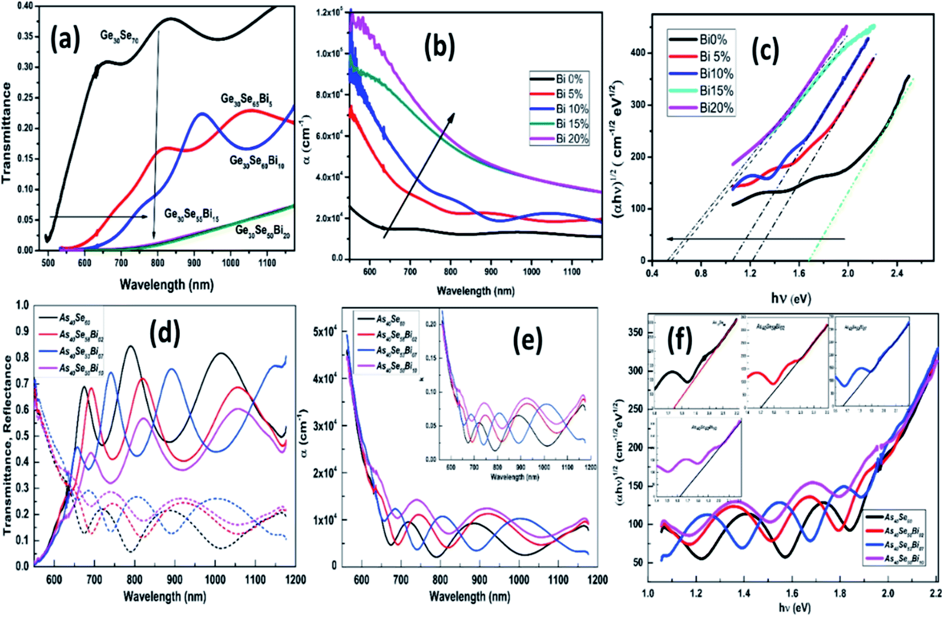 | ||
| Fig. 1 (a) The transmittance (b) absorption coefficient (α) (c) (αhν)1/2 vs. hν (eV) variation for Ge30Se70−xBix film,38 (d) the change in transmittance (e) absorption coefficient, and extinction coefficient (inset plot) (f) optical bandgap of As40Se60−xBix thin films.39 | ||
The investigation on the effect of Bi atoms through different property modifications of Ge20BixSe80−x films was studied by A. El-Korashy et al.40 The behavior of the optical bandgap of the Ge–Se–Bi composite thin layers clearly showed a significant decrease (from 2.62 to 1.24 eV) with the increase in Bi content from x = 0 to x = 25. This behavior is due to the improvement in defect density on the bandwidth area due to the increase in Bi content. The variation of activation energy in Ge20BixSe80−x thin films showed a decreased pattern for effective Bi content. This behavior was due to the unpinning and fluctuation of the Fermi level Ef position towards the conduction band, resulting in the origin of n-type conduction. However, H. El-Zahed41 showed that the dependence of Eg as a function of film composition for Ge20BixSe80−x (x = 0, 5, 9, 10, 15, 20, and 25) was obtained at ambient temperature. The result showed a significant decrease in the optical bandgap from 2.1 to 1.65 eV as the content of Bi increases to 10 at%. However, further addition of Bi causes a minimal change in Eg. Likewise, the reciprocal temperature dependency of resistivity (ρ) of Ge20BixSe80−x films decreases with an increase in temperature. This behavior obeys ρ = ρ0![[thin space (1/6-em)]](https://www.rsc.org/images/entities/char_2009.gif) exp(ΔE/kT), where ρ0 is the pre-exponential factor, ΔE is the electrical activation energy, and k is the Boltzmann's constant. As a result of the majority load carrier change, a change in electrical conductivity was observed for 10% Bi doping in the Ge–Se system. So, x < 10 showed band conduction, and x ≥ 10 showed hopping conduction in the localized state.
exp(ΔE/kT), where ρ0 is the pre-exponential factor, ΔE is the electrical activation energy, and k is the Boltzmann's constant. As a result of the majority load carrier change, a change in electrical conductivity was observed for 10% Bi doping in the Ge–Se system. So, x < 10 showed band conduction, and x ≥ 10 showed hopping conduction in the localized state.
Chalcogenide materials have shown different properties like high refractive index (n > 2) and high NIR transmission, making it more fascinating to apply. These unique properties are easily influenced by doping with suitable metal atoms. Bi integration into the Ge–Se matrix improves chemical sustainability. Replacing Se with Bi results in a decrease in the optical band interval and increases the transmission property on the mid-IR region of the Ge–Se system.42 Considering the In25−xBixSe75 (x = 0, 1, 3, 5, 7) system, it has been seen that for higher concentration (x > 7) of Bi leads to the appearance of the Bi2Se3 phase in the annealed films. The temperature dependence study of dc electrical conductivity revealed the observation of hopping conduction at x = 3% of Bi content, while the observation of significant change at x > 5 that due to extended state conduction with the increase in the doping concentration. Moreover, this behavior leads to an increase in the state of disorder and defects, resulting in a decrease in the optical bandwidth gap of the system. This incorporation also leads to a change in conductivity due to the switching conductivity from hopping conduction to the extended state conduction.43
Factors like density, electronegativity, atomic radius were mainly affected due to the doping effects of metal-induced chalcogenide materials. Considering the incorporation of a high concentration Bi in the Se–Te alloy system causes an increase in the band tailing states by a decrease in optical bandgap due to widening the valence band.44 The increase in Bi concentration also regulates specific heat and heat capacity. Due to the absorption of heat energy by a large number of degrees of freedom, a decrease in specific heat and heat capacity has been observed with an increase in Bi concentration.45
The comparative variation in the behavior of chalcogenide materials due to Bi doping has been demonstrated in Fig. 2. In Fig. 2, we have shown the comparative effect of Bi introduction on absorption coefficient (α) and energy gap (Eg) for Ge–Se, In–Se, and As–S films, respectively. The introduction of bismuth as a bilayer caused by annealing and irradiation significantly alters the optical properties. The Bi doping in the As–Se system results in the enhancement of density of states (DOS), creates localized states in the forbidden gap and affects the surface structure. Bi doping reduces the optical bandgap because of the formation of homopolar bonds (Bi–Bi) at the interface of the bilayer structure.46 Fig. 2(a) and (b) present the optical changes due to Bi layer deposition over As2S3 thin film. The reduction of Eg is due to localized states on the bandwidth area which eventually improves the absorption capacity. During laser illumination, the phenomenon of photobleaching was observed in the Bi/As2S3 film that induces the photographic diffusion of Bi in the As2S3 matrix by forming several new dangling bonds. However, in the case of GeSe2 film,47 Bi introduction and post energy introduction result in the formation of the Bi2Se3 phase by causing phase transformation. This transition causes dangling surface bonds around the crystals due to the energy-induced diffusion process. Thus, Fig. 2(c) and (d) reflect the consequences of phase transformation due to the incorporation of Bi layers in the Ge–Se matrix and post-annealing and laser-induced scattering, respectively. Similar behavior has also been observed with the Bi/In2Se3 bilayer film. The subject of Bi layer over In–Se matrix results in a decrease of the optical bandgap, while annealing and laser irradiation results in the increase of energy gap by forming Bi–In–Se diffused glassy matrix.48 The increase in the absorption coefficient with the addition of Bi is observed in Fig. 2(e), showing the reduction in transparency across the wavelength range. The variation in the refractive index of the Bi/In2Se3 bilayer films was shown in the Fig. 2(f). In the chalcogenide and pnictogens materials, the lone pair orbitals from the valence and conduction bands are formed by the antibonding orbitals. The exposure of high-energy radiations results in the excitation of the electrons from lone pair and bonding states to higher energy states. The outer electrons immediately fill the vacancies created in these states through the Auger process, which induces more holes in the lone pair and bonding orbitals, leading to a vacancy cascade process. Throughout these processes, bond-breaking ionization of atoms easily occurred, leading to a change in the glassy network's local structural order, resulting in the system's change in refractive index and extinction coefficient.49 Here, the variation means the incident radiation loss in the whole medium increases with the addition of Bi and its diffusion through the introduction of energy.
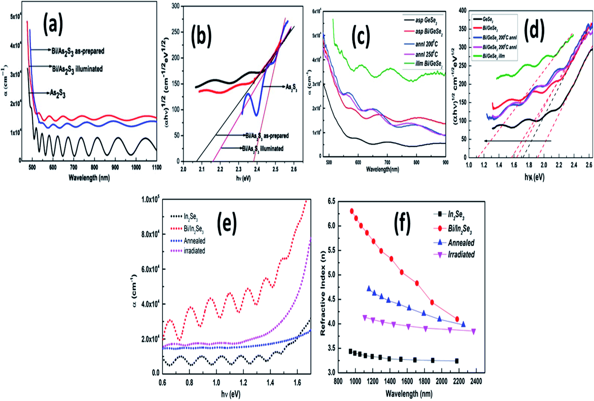 | ||
| Fig. 2 (a) The transmittance spectra dependence behavior over wavelength and (b) (αhν)1/2 vs. hν (eV) variation for Bi/As2S3 films46. (c) The transmission change and (d) bandgap variation for Bi/GeSe2 film,47 (e) the transmittance and (f) refractive index spectral behavior over wavelength and energy of Bi/In2Se3 thin films.48 | ||
The sequential evidence of the addition of Bi in the Se matrix was analyzed in the BixSe1−x thin films made by M. A. Majeed Khan et al.50 The transmittance showed an increment behavior with an increase in Bi concentration from 0 to 2.5 at% then decreased afterward increase in Bi content, i.e., for 5% Bi-doped film. This behavior is due to the doping of higher content of bismuth that results in the entering of Bi atoms into the ring structure of selenium atoms which could decrease the transmittance by shifting the K-edge shift of Se. Similarly, the decrease in the optical bandgap with Bi concentration is due to the red-shifting of the absorption edge. The overall decrease in the optical band interval is due to the creation of localized states with the increase in Bi concentrations. The energy gap reduction is attributed to the rise in the density of defects and the decline of the bond energy value on average. The short-range order and the formation of Se–Bi bonds are directly responsible for such observable behavior. The conductivity at a low concentration of Bi decreases whereas at a high concentration of Bi there is the appearance of a sudden increase of the conductivity.
The nonlinear refractive index of the chalcogenide system comes into play when exposed to the strong electromagnetic field that can be explained through the polarization of atoms and distortion of electron orbits. In the course of nonlinear effect in the glassy matrix, the important role has been played by lone pair orbitals of chalcogens (S, Se, and Te) and pnictogens (As, Sb, Bi…etc.) showed easy polarizability. It has been observed experimentally that the dependency over nonlinear effects on lone pair concentration or, more precisely, the concentration of atoms with lone pairs is more prominent such as replacing Se (with lone pair) with Ge (no lone pair) doesn't influence the value of the nonlinear refractive index (n2) in Ge–Se system. Similarly, replacing Bi (same lone pair electrons as Se but higher polarizability) at the place of Se (less polarizability) showed enhancement in nonlinear refractive index and third-order susceptibility of the system.3 This can be explained by the increase in the nonlinear refraction index due to the doping effect of Bi in the Se–Te. The nonlinear refractive index showed a reduced trend, whereas β2 showed an increasing trend with Eg. As the Bi increases, the density of the glass network increases in a monotonous manner. As with high density and larger radius compared with Se and Te, a higher concentration of Bi enhances the polarizability of the system, which ultimately affects the nonlinearity.51
According to Takats et al., a change of optical properties has been observed in the Bi(Sb)/As2Se3 bilayer structure, making it useful for application in amplitude modulated optical records.52 Dielectric relaxation is related to dielectric losses, allowing for easy understanding of structural changes and defects in chalcogenide systems.
Metal doping in chalcogenide systems also affects the refractive index of host systems. The refractive index depends on the polarizability of the elements. The integration of Bi into chalcogenide systems makes it possible to produce a powerful containment of the electric field that allows the system to be used for optical waveguide applications with a compact design of the area and high intensity. This increase in the refractive index is due to the rise in polarizability and increased Bi concentration in composition.53 From the literature survey, it has been found that the refractive index is related to transmittance. The increased range of transmission is ascribed to an increased refractive index. This increase in the refractive index is ascribed due to the increase in the compactness due to the replacement of higher density Bi (9.8 gm cm−3 at 20 °C) at the position of low-density Se (4.79 gm cm−3 at 20 °C).54 Due to the laser-induced effect, a change in the chemical and structural properties results in the tailoring of the refractive index of the Bi-doped As40Se60 system. The conversion of homopolar bonds to heteropolar bonds results in structural disorder due to illumination. Laser illumination reduces the refractive index and improves the bandwidth deviation from the one prepared. This behavior is due to structural modification due to the change in the defect states.55
Bismuth-doped manganese indium sulfide (MnInS4) thin films were synthesized using the spray pyrolysis technique. The films were deposited with different substrate temperatures from 250 °C to 400 °C with constant spray time. With the increase in substrate temperature, the film thickness decreases with decrease in scattering centers and defect density. The PL spectra observed showed excitation wavelength from 350 to 650 nm, corresponding to blue, green, yellow, orange, and red band emissions. The appearance of those peaks was due to the band edge emissions and defect emissions. It has been observed that the intensity of the peaks enhanced with an increased substrate temperature which might be due to the reduction in defect states and strain. This could be attributed to the improvement in the crystallinity of the material films.56 The photoluminescence technique plays an essential role in extensive research on thin films' energy levels. For the Sb2S3/Bi bilayer film, the PL spectra showed a strong emission at 335 nm, attributed to the photon-assisted transitions and the recombination of the electronic hole after relaxation (band edge emission).
Similarly, a weak emission peak at 686 nm contributed to the emission of recombination of electrons and holes trapped in surface states localized in the forbidden region of the bandgap. The intensity enhanced with Bi doping was due to the crystalline size, as the PL intensity is mainly the inverse of the square of the crystalline size. All emissions were associated with defects that occurred during crystalline growth and were also linked to crystalline deformation due to dislocation and large vacancies.57
The cm3 thin films were successfully prepared by chemical bath deposition technique, which showed significant change in lattice parameters and crystallite size with varying Bi concentration in the films. Photoluminescence (PL) studies showed that PL peaks shift to a higher wavelength with Bi doping concentration. By adding Bi foreign element, the CdS film results in the displacement of the interstitial position of the CdS network, which causes an important level of structural disorder on doping. The slight shifting of peak maxima towards longer wavelength regions is mainly due to the indirect recombination of the free electrons moving from the trap level formed by the Bi atoms to the holes in the valence band. It has been observed that the film deposited with a higher Bi concentration showed maximum PL intensity.58
2.2. Antimony doped chalcogenide films
Metal-doped chalcogenide films have developed into a potentially emerging class of non-crystalline semiconductors in the science and technology industry. The divergence of excellent transmission over near and far IR spectral regions allows these materials to have a significant role in the field of optoelectronic device applications. The addition of metals in the host matrix is intended to change optical and physical parameters because new defects are created inside the glass network. Among such metals, antimony (Sb) is well known for creating such defects in the network, and also it significantly influences the short and medium-range order in the glassy network of films that further causes the tailoring of properties. Along with bismuth, antimony also unpins the Fermi level, supporting the carrier type reversal, i.e., p ↔ n in the glass matrix. This transformation enables the glass area to be enlarged, the thermal stability to be improved and the IR transmission to be increased. Thus, the Sb doping results in remarkable multifunctional material for several applications. It is also observed that Sb acts as a chemical modifier and results in the creation of disorders. Hence, modifications in the structures of chemical composition happen by keeping the application point of view.30,59,60 For example, the compositional influence of Sb doping in Ge15−xSbxSe35Te50 thin films enhances the absorbance capability by shifting the absorption edge towards a higher wavelength. This behavior is primarily because of the solid metallic characteristic of antimony with a larger atomic volume than Ge, which increases the electronic polarizability, ultimately enhancing the loss of incident radiation through absorbance. However, the Sb doping decreases the valence bond potential, increasing the conduction band potential. Hence, this doping effect drives the corresponding valence levels closer to the Fermi level and decreases the transition width and transition energy of electrons, respectively.59 The lone pair electrons in chalcogenide and pnictogens elements also impact the bandgap variation via doping and external energy inputs. As we know, the valence band is mainly constituted by lone pair (LP) orbitals. With the exposer of higher incident energy, the electrons from the top valence band are moved to the conduction band, leaving the unpaired electron in the former LP orbitals. Simultaneously, an additional bond formed with the excited electron with electrons from other atoms will create a neutrally dynamical interchain bond that will create local distortions and change the defects and disorder inside the system, contributing to the change in bandgap.60Similarly, the consequence of Sb incorporation on the optical parameters for the amorphous Ge–Sb–Se–Te thin films has been studied by A. S. Hassanien. It has been observed that the replacement of Sb at the position of Ge results in an increase of optical band energy with Sb content. At the same time, electronegativity was found to be decreased. The Sb doping enhances the free charge carrier concentration by strongly contributing to the polarization process. The addition of Sb at the place of Ge reduces the transmittance optical energy and increases the reflection due to antimony's silver and lustrous dark gray metalloid appearance.61 The thermoelectric power factor of vacuum deposited In2Te3 has been dramatically improved, i.e., 8.7 times with 1% Sb doping than un-doped film. Hence Sb doping showed more favorability to enhance the thermoelectric performance of In2Te3 films.62 The consequent effect of Sb concentration on the linear and nonlinear optical properties of Ge–Se–Sb films has been investigated by Z. Z. Ying et al. The nonlinear optical properties observed from the Z-scan technique get enhanced with the increase in Sb concentration. The value of the nonlinear refractive index (n2) and absorption coefficient (β) of the Sb doped Ge–Se film showed of the order of 10−18 m2 W−1 and 10−10 m W−1, which is much greater than host Ge–Se films.63 However, the investigation on the possibility of Ge–Se–Sb film for phase change recording media has been investigated by F. A. Al-Agel. The optical energy gap decreased with Sb doping due to the enhancement of defects over the gap region.64 Antimony doping changes the glassy network that affects the physical properties such as the atomic density, molar volume, molar mass, which showed increment with the substitution of Sb, whereas compactness, interatomic radius, packing density decrease. Antimony substitution enhances the polarizability of the atom that affects the refractive index and other related optical parameters.30,59 The optical bandgap shrinks with the addition of Sb in the thermally evaporated Ge20Te80−xSbx (x = 0,2,4,6,10) thin films due to the compositional change in the host network that in turn affects the bond angles and bond lengths. It is noticed that the antimony rich system, i.e., Ge20Te70Sb10 sample showed a high value of the nonlinear refractive index, n2 (12.3 × 10⁻¹⁷ m2 W−1) and third-order susceptibility, χ(3) (2.43 × 10⁻¹² esu), which is 1000 times higher than that of silica.65 Mishra et al. analyzed the optical and structural characteristics of Sb doped (Ge11.5Se67.5Te12.5)100−xSbx (0 ≤ x ≤ 30) glasses. Doping Sb with different concentrations expands the glass-forming ability, creates disorder, and modifies the glass matrix of the host system.66
The deposition of the Sb layer onto As2Se3 film with post-photo diffusion effect has been observed in Fig. 3(a) and (b). The transmittance decreased from 67% to 52% with the deposition of Sb diffusion into the As–Se matrix. It is observed that subsequent photo diffusion, the absorption edge shifts to higher photon energy that enhances the creation of homopolar bonds during Sb diffusion, improving the density of defect states. It decreases the optical bandgap with Sb addition to As2Se3 film, as shown in Fig. 3(b).67 Besides that, the composition variation in As2−xS3−xSbx (x = 2, 7, 10, 15) film showed the mechanical mixture of two-phase As2S3 and Sb2S3 with considerable variation in the optical behavior. The apparent decrease in the transmittance from Fig. 3(c) and the red shifting of absorption edge with Sb content indicates the absorbance of incident radiation while traversing throughout the As2−xS3−xSbx film + Fig. 3(d).68 Similarly, the composition variation in Sb doping in the different matrices such as As–Se and Se–S has been observed in the rest of Fig. 3(e–h). Transmittance spectra correspond to As40Se60−xSbx film (Fig. 3(e)) showed the decreased pattern, whereas the reverse has been observed in the case of SbxS40Se60−x film (Fig. 3(g)). But both the optical energy gap reduced with increasing S content as the creation of localized states in the bandgap.69,70 E. R. Shaaban has done a similar investigation on the compositional variation of SbxGe25−xSe75 semiconducting film. Optical parameters such as the refractive index gradually improved with the increase in Sb content due to the increased polarizability of the high atomic radius Sb (1.38 Å) as Ge. Additionally, the Sb doping greatly influences the optical band structure, leading to changes in the optical characteristics and making those samples worth possible for several optoelectronic device applications.71
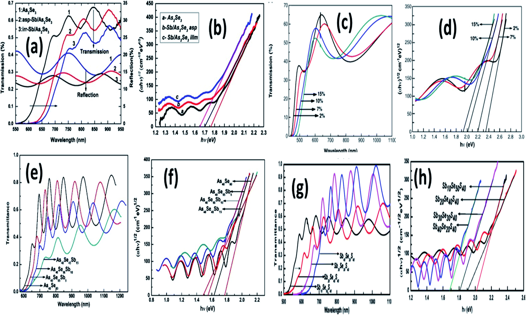 | ||
| Fig. 3 (a) The transmittance and (b) optical bandgap variation in as-prepared and irradiated Sn/As2Se3 thin films.67 The Sb doping variation in (c) transmittance behavior and (d) optical energy gap of As2−xS3−xSbx thin film, respectively.68 The compositional variation for Sb doped As40Se60−xSbx thin film in (e) transmittance and (f) optical energy gap behavior.69 (g) The transmittance and (h) optical energy gap behavior for SbxS40Se60−x thin films with different dopant concentrations.70 | ||
In addition to the optical and structural behavior, Sb doping is much more useful for controlling the morphology of polycrystalline chalcogenide materials. Crystal aggregation with cross-linked grain coalescence was observed with doping Sb. However, with further Sb addition, those crystallites were broken down to form nanocrystalline particles with a significant influence on the alteration of optical statistics.72 The effect on physical properties of Sb doping in CdSe film has been investigated by M. Ali et al. The incorporation of antimony results in structural changes such as a decrease in grain size that causes discrimination in electron diffusion. This results in an increase in conductivity and change in optical entities, such as the decrease in optical band energy and an increase in absorption that makes it more suitable for solar cell applications.73
Thin layers of cadmium selenium (CdSe) doped with different concentrations of antimony prepared by the electron beam evaporation technique were investigated by S. Mathuri. The transmittance of the CdSe films showed a reduced pattern with various amounts of Sb content, and an enhancement in the optical bandgap from 1.74 eV to 2.3 eV has also been observed. PL study showed two broad peaks at 605 nm and 743 nm, in which the former one corresponds to absorption edge, and the latter corresponds to electron–hole pair recombination. The band's intensity varies with respect to the Sb content such that the 5% and 10% Sb doped film showed higher intensity with host CdSe matrix and then for 15% doped film showed decreased intensity and further increased for 20% Sb. These changes in PL intensity and the transition to a higher wavelength range could be due to the change in the crystalline size with doping Sb.74 Similarly, four emission peaks (470–540 nm) were seen in Sb-doped CuInS2 films. These peaks essentially represent the transition of the donor–acceptor pair between the elements present. PL peak widening based on substrate temperature was attributed to a high defect concentration. The broad emissions were typically for the non-equilibrium process for film growth and results in disorder on cation sublattice. All emissions were associated with defects arising from crystalline growth and deformation due to dislocation. Compared with the undoped one, the Sb doped CuInSe2 PL spectra showed blue and green band emissions.75
2.3. Silver doped chalcogenide thin films
The addition of metals to the chalcogenide system contributes primarily to the formation of cross-linked structures and enhances other physical properties. Incorporating silver (Ag) in the chalcogenide material enhances the electrical conductivity and Ag alloys by crossing over the chalcogenide chains and making the system stable. Due to potential applications of devices in chemistry, optoelectronics, biology, and optics such as optical memories, microlenses, waveguides, networks, sensors, etc. silver-doped chalcogenide films have been given abundant attention in glass science and technology. Due to the ionic character, the introduction of Ag results in different structural alterations in the materials, which in turn modifies the band structure and hence the electrical properties of the material.76–92 For example, the increase in Ag concentration doping in the Ge–S system (x = 57.1 at%) enhances the conductivity of the order of 22 times of the doping concentration (x = 30 at%) Ag in the same system.76 This enhancement of conductivity is due to the ionic character of Ag+ ions. It has been seen that increasing the concentration of Ag in chalcogenide glasses, i.e., from 5 at% of Ag to 30 at% of the same system, modifies from ionic conductor76,77 to superionic conductor system.78In chalcogenides, the photoinduced effect is very influential due to the impact of the localized state present in the middle of the bandwidth gap. These photo-doped metal chalcogenide films were useful in the application of holographic recording. The change in thickness of the metal-doped chalcogenide material due to photo induction is insignificant. Considering the photodoping of Ag in As–S and As–S–Te systems enhances the optical absorbance. This enhancement is due to the diffusion of the Ag layer in the host materials and forming heteropolar bonds.79,80 For high-speed optical communication, nonlinearity is considered to be the key ingredient. But the nonlinearity demonstrated by silica glass is small, so to be used for switching and communicational application, either long device length or a more excellent power supply are required. Thus, materials with high nonlinearity are necessary to produce nonlinear photonic circuits with low threshold and condensing. Chalcogenide materials are highly nonlinear and offered for switching in telecommunication applications.81 Chalcogenide materials possess nonlinear susceptibility, two orders of magnitude higher than silica. These nonlinear properties become active when they are influenced by a strong electric field. This nonlinearity demonstrated by chalcogenide is greatly affected by the doping effect resulting from the subsequent change in the material system. The nonlinear property of Zn–S thin films gets enhanced by Ag doping. It was found that as the concentration of Ag increased, the nonlinear refractive index increased. This increase contributed to the rise of linear absorption of the film due to the increase in Ag ions.82 Since the nonlinear properties are internally connected with the nonlinear polarization and incident radiation, the subsequent annealing and illumination after the doping of Ag in the Ge–S system enhance the nonlinearity. This behavior is attributed to the diffusion of Ag in the Ge–S layer.83 But opposite behaviors were observed for Te doping in the Cd–S system. The doping effect effectively reduces nonlinear properties. This decrease in nonlinearity is due to the alteration in polarization in the system.84
The photo-induced dissolution and diffusion of Ag metals in chalcogenide films showed superior diffraction effectiveness. According to T. Wagner,85 the rate of optically induced diffusion and dissolution of silver is higher in multilayer structures than in bilayer films. Grating formation by holographic exposure of multilayer specimens Ag/As30S70 confirmed five times more sensitive than prepared bilayer films. The linear and nonlinear alterations resulting from Ag layer deposition and diffusion have been shown in Fig. 4, respectively. Ag diffusion into the GeS layer increased the optical bandgap with no structural transformation, primarily due to decreased width of localized states. The transmittance increased to 37% from 27% with just deposition of Ag metal, which corresponds to its metallic behavior by providing a large number of charge carriers. Further laser and annealing induced diffusion increased 43% and 47%, respectively, as shown in Fig. 4(a).83 Consequently, the decrease in refractive index upon annealing and laser irradiation in Fig. 4(b) also supports this behavior. The monotonous increment of nonlinear susceptibility with scattering Ag in Fig. 4(c) showed the usefulness of UV nonlinear optical materials, solid-state laser, etc. In other words, the Ag layer deposition on Se film decreases the transmittance, as shown from Fig. 4(d).86 Such reduction in transmittance power provides a clear indication of the diffusion of Ag into the Se layer. The significantly decreased annealed film is primarily due to Raleigh light scattering and increased absorption power. This gets the confirmation from the refractive index behavior in Fig. 4(e). The nonlinear susceptibility related to the polarizability increases monotonically with a decrease in the bandgap observed from Fig. 4(f) which may be due to the change in the defects and disorder. The Ag deposition and diffusion in the Se matrix increases the nonlinear phenomenon inside the matrix, making it suitable for nonlinear optical devices.
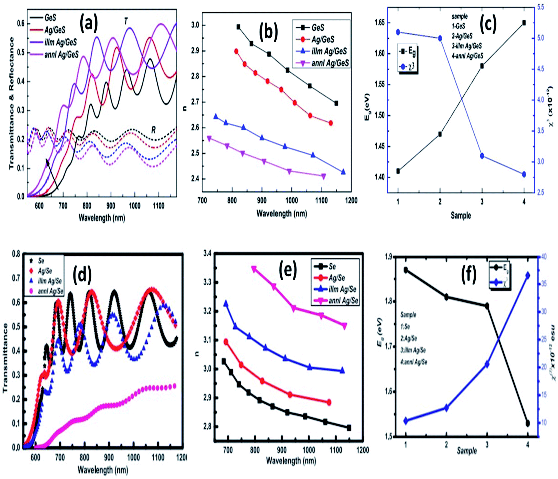 | ||
| Fig. 4 (a) Transmittance and reflectance spectra of Ag/GeS as-prepared and illuminated thin films, (b) refractive index dispersion behavior of the Ag/GeS thin films, (c) variation of Eg and χ(3) with bilayer Ag/GeS film,83 (d) transmittance spectra (e) refractive index variation and (f) band energy with nonlinear susceptibility of Ag/Se bilayer thin films.86 | ||
Defect states also enhance the nonlinear opticals of the system. This behavior has been seen in the Ag-doped Ge–Se–Sb system. The Ag concentration in Ge–Se–Sb film improves the nonlinear absorptions that ultimately form the mid-gap states known as the localized defect states. A clear redshift in the transmission spectra and an increase in the amplitude of the interference fringes in the Ge–Se–Sb–Ag films inevitably cause an increase in the refractive index.87 In Ge–Sb–Te (GST) ternary film, the GeTe–Sb2Te3 pseudo-binary tie-line enhances the thermal stability, but crystalline speed decreases. According to the literature, GeTe has a high thermal strength but a low crystalline speed; on the other hand, Sb2Te3 maintains a low thermal stability but a high crystalline speed. Therefore, the Ge2Sb2Te5 (GST) played a middle-man candidate by forming the GeTe–Sb2Te3 pseudo-binary phase, the tie line that showed excellent thermal stability and good crystalline speed, scalability, and reliability. Thus, it is one of the best phase change materials.88,89 Doping in this phase change material has shown great potential to be used for device applications. According to Song et al.,88 the Ag doping in GST enhances the crystalline speed from 67 to 30 ns and the sheet resistance to its ten times in the amorphous phase. Phase change materials possess several fascinating properties that could be critically applicable for many applications, including the resistance contrast, transport speed between an amorphous and crystalline state, and material dependence of the switching characteristics. Ag doping in GST thin films enhances the optical energy gap, significantly reducing threshold current that enhances switching speed and provides better thermal stability.89 For (Ge2Sb2Te5)100−xAgx thin films, the doping of 3% Ag showed maximum average transmission over the NIR range, confirming the minimum density of defect states. The absorption edge is shifted towards a lower wavelength (blue shift) until 3% Ag doping and then shifted towards a longer wavelength (redshift) for a higher percentage of Ag doping. Consequently, the optical bandgap increases with Ag doping up to 3%, and then it decreases for higher Ag content.89 Ag doping in the (Ge2Sb2Te5)100−xAgx system mainly influences the nonlinearity by decreasing the nonlinear susceptibility up to x = 3 at% and then increases due to the distortion in the host matrix because of the high concentration of Ag. This variation is mainly caused by the phase change between amorphous and crystalline, which allows the system to customize several properties. The interpretation of electronegativity and nonlinear optical susceptibility with Ag content at 1500 nm wavelength showed a decreasing trend with doping concentration up to 3%; after that, it starts increasing due to distortion in the host matrix at higher doping concentration. The conductivity increases with the increase in the energy in the energy of incident light due to the excitation of thin-film electrons. With Ag addition in Ge2Sb2Te5 up to 3%, optical conductivity decreases, and 10% Ag doping optical conductivity increases.90
Furthermore, the silver doped In2Se3:Ag thin films were synthesized by the spray pyrolysis method at 350 °C to analyze the corresponding physicochemical properties of the films. Polycrystalline film peaks with the appearance of the β-In2Se3 cubical phase confirmed by the XRD and Raman study. The optical absorption showed opacity above the UV region and transmission above the visible and near-infrared region of the electromagnetic spectrum. The PL spectrum observed showed improvement in peak intensity with Ag doping up to 4%, then decreased with higher Ag doping content. The PL intensity and crystallite size showed proportionality towards each other with respect to Ag content. Crystallization leads to higher recombination of the electron–hole pair that has improved the intensity of PL.91 Similarly, the photoluminescence properties of Ag doped ZnxCd1−xS quantum dot thin films were strongly influenced by Ag doping content, sintering temperature, and time. The PL peak changes from 559 nm to 572 nm with an increase in Ag content from 0.1% to 0.5%. For 1.0% Ag, the observed PL intensity showed a maximum value. Also, it showed the PL intensity shifted with sintering temperature due to the increase of particle size with an increase in reaction temperature.92
2.4. Tin doped chalcogenide thin films
Considerable efforts have been made to synthesize and characterize metal-doped chalcogenides. Among all transition metals, tin (Sn) is well susceptible to the formation of tetrahedrally coordinated sites. It significantly influences the host matrix's network connectivity by inducing short- and medium-range alterations. As a dopant, tin serves as a model probe atom to permit local structure changes characterization of the impurity in chalcogenide glass.93–104 For example, doping of a high concentration of Sn in the As–Se system causes an increase in the growth of the tetrahedral unit of structure Sn(Se1/2)4.93 Tin as an impurity significantly influences the absorption edge, causing the exponential slope to decrease, widening the spectral range of photoconductivity, and delaying the recombination of the photogenerated holes. The optical study under light exposure in amorphous films As2Se3 doped with Sn (0.5 to 5.0 at% Sn) was studied by M. S. Iovu and his co-authors. It was shown that it effectively reduces photodarkening and this degree of reduction becomes stronger up to 2.0% concentration, then photodarkening increases again. The doping of amorphous chalcogenide films by tin serves as a stabilizer for stabilizing the glass matrix in terms of light exposure and heat treatment.94Recently, special attention has been given to the preparation and characterization of thin films of doped chalcogeneration such as CdSe, CdS, etc. Among these, the CdSe thin film belongs to the semi-conductor group II–VI with a direct bandgap of 1.74 eV, tunable and excellent optical and electrical properties. Thus, the study on the incorporation of Sn in thin layers of nanocrystalline CdSe by the chemical bath deposition technique was performed by P. K. Sahu and his co-authors. It has been observed that the crystallinity behavior of the films is enhanced by doping Sn due to an increase in the grain size. Sn incorporation in CdSe decreases the optical bandgap from 2.62 eV (undoped CdSe) to 2.50 eV (5% Sn:CdSe) respectively. This increase in grain size with Sn doping significantly decreases the electrical resistivity.95
Here, in Fig. 5(a), the bandgap Eg was calculated using Tauc's relation for direct transition type. The observed optical bandgap values showed reduced order from 2.62 eV to 2.50 eV while going for the undoped film to Sn doped film with different percentages. The variation in bandgap energy might be due to the variation in structure and size of grains of the Sn doped CdSe films. The increase of the doping density causes the broadening of the intragap impurity bands. Upon Sn doping results in a bandgap reduction while increasing optical absorbance and absorption coefficient. Fig. 5(b) presents log(ρ) versus inverse absolute temperature. With an increase in the temperature, the resistivity decreases, confirming the films' semiconducting nature. The low-temperature resistivity at 323 K of the undoped CdSe and doped (1%, 2%, 3%) Sn: CdSe thin films were in the range of 107–104 Ω.cm. Photoluminescence analysis offers a non-contact, non-destructive and authentic method for optical investigation. In Fig. 5(c) showed the PL emission spectra of Sn doped CdSe thin films. This plot clearly showed the intensity variation with Sn doping due to the modifications in crystalline structure and increased crystalline size. This includes the luminescence is due to band–band transition and electron–hole recombination involving levels in the bandgap due to Sn addition.95
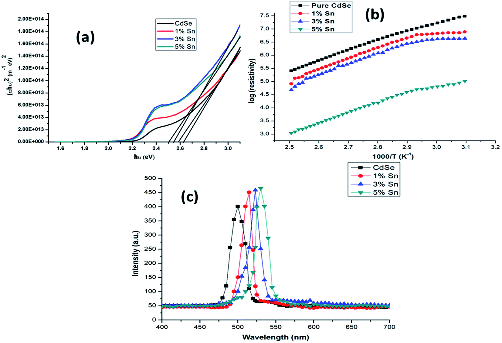 | ||
| Fig. 5 (a) Plot of (αhν)2 vs. energy (hν) for the undoped and Sn doped CdSe thin films which showed a decreased pattern with different doping percentage, (b) plot of log(resistivity) with the inverse of absolute temperature for the undoped and Sn doped CdSe thin films, (c) photoluminescence emission spectra of undoped and Sn doped CdSe thin films at room temperature showing the variation in the intensity concerning doping percentage.95 | ||
Similarly, the linear and nonlinear refractive index study of Sn doped Se–Te–Bi chalcogenide films has been done by P. Yadav and A. Sharma. Sn doped thin films' linear and nonlinear refractive index has incrementally with Sn content. Sn doping significantly increases the transmission in the Se84−xTe15Bi1.0Snx (x = 0, 2, 4, 6, 8) thin films.96 Sn doping in phase change material, Ge–Sb–Te (GST) thin-film, has a slightly lower crystallization temperature than the host GST. These doped materials showed ultra-fast crystallization with reduced activation energy and enhanced signal-to-noise ratio and recording in phase change storage resulting from doping Sn.97 It has been seen that introduction of Sn in the Ge1−xSnxS3 (x = 0, 0.2, 0.4, 0.6) system decreases the threshold voltage value with the concentration of Sn, and this leads to the increase in the switching current during off state and also it has been observed that the thickness increases accordingly with respect with the increase in threshold voltage values. Furthermore, the introduction of Sn in the Ge1−xSnxSe3 system results in the shifting of band-edge with an increase in x values as Sn has substituted at the position of Ge. This indicates a decrease of bandgap with an increase in Sn concentration. This behavior is due to the intrinsic defect states contributed to the deposition of Sn. The shifting behavior of the refractive index towards the lower energy values is attributed to the increase of Sn concentration in the Ge1−xSnxSe3 system.23 A decrease in the conductivity value has also been observed at x = 0.4 for system Ge1−xSnxSe3 by doping Sn due to the hopping conductivity at the unoccupied localized states, and the conductivity enhanced with further increase in the concentration Sn values. The thin film composition Snx (Sb0.70Te0.30)100−x (with x = 0, 2.5, 5.0, 7.5 at%) deposited by pulsed laser deposition has been studied by V. Bilovol and his co-authors. Their structural and electrical behavior with temperature has been studied to analyze the phase transformation. Sb70Te30 crystallizes in a trigonal P![[3 with combining macron]](https://www.rsc.org/images/entities/char_0033_0304.gif) m1 space group structure while doping with Sn leads to structural distortion of the unit cell. The presence of Sn induces an acceptor impurity level in the electronic band structure of Sb70Te30. So, the doped system showed a direct bandgap semiconductor in the order of 0.3 eV and independent of the dopant concentration.98
m1 space group structure while doping with Sn leads to structural distortion of the unit cell. The presence of Sn induces an acceptor impurity level in the electronic band structure of Sb70Te30. So, the doped system showed a direct bandgap semiconductor in the order of 0.3 eV and independent of the dopant concentration.98
The nonlinear behavior has also been seen to be influenced by Sn doping. For example, an increase in the Sn doping concentration in the Ge–Se system enhances the nonlinear susceptibility (from 0.5 × 10⁻¹¹ to 7.5 × 10⁻¹¹ esu). This behavior is due to the different absorption edges formed due to the change in composition. The Sn doping also affects linear optical properties effectively, as shown from the above Fig. 6. Fig. 6(a) depicts the transmission spectra of GeSe2−xSnx (0 ≤ x ≤ 8). The figure shows that at λ > 850 nm, all the films became transparent, indicating a lower diffusion and absorption; therefore, the transmission intensity is 80% higher than the intensity on the visible region. In addition, the absorption edge increased showed redshift with Sn dopant concentration increase. The effect of film composition on the spectral behavior of the dispersion curves is shown in Fig. 6(b). The refractive index (n) for all films increases with an increase in λ up to 800 nm. After that, it decreases with the increase of wavelength. This increase in n value with an increase in doping concentration could be ascribed towards an increase in the valence of the current carriers. This refers to the increase in polarizability associated with larger Sn atoms. The bandgap value estimation for Sn doped GeSe using Tauc relation is shown in Fig. 6(c). The addition of Sn atoms at the place of Se atoms induces the formation of Ge–Sn and Sn–Sn bonds at the place of some Ge–Se bonds. This indicates an increase in the density of weaker bonds at the expanse of stronger bonds because of the higher atomic weight of an Sn atom than that of a Se atom. This consequently decreases the optical bandgap energy of GeSe2−xSnx by increasing the Sn content.99 Similar behaviors have also been seen for Sb doping in the GeSe2 thin film.100
 | ||
| Fig. 6 (a) Optical transmission (T) of GeSe2−xSnx films (0 ≤ x ≤ 0.8) as a function of wavelength of light λ, (b) variation of refractive index (n) against wavelength (c) (αhν)1/2 versus hν for GeSe2−xSnx films.99 | ||
Similarly, the change in the optical properties due to Sn doping in Sb2Se3 has been investigated by F. Aousgi and M. Kanzari. The refractive index and extinction coefficient of host materials were dependent on the Sn% molecular weight. The refractive index decreases from 3.2–2.8 at λ = 0.7 μm to 2.9–2.7 at λ = 1 μm. By increasing the Sn content, the carrier concentration to effective mass ratio (N m−1*) increases.101 A similar study on Sn doped SbSe film deposited by chemical bath deposition method has done by S. Mushtaq and his colleagues. Their optical measurement showed a broad range of direct bandgap in 1.45–1.80 eV with a refractive index of 3.38–6.39. The doped films showed significantly high photo-response and electrical conductivity values over the range of typical electrical conductivity values for semiconductors. The deposited film's good absorbance property showed the possibility of being used for solar cell applications.102
Tin-doped In2S3 films synthesized by chemical spray pyrolysis have a polycrystalline nature and a significant influence on the optical characteristics of the matrix. In2S3:Sn films have a transparency greater than 60–85% in visible and infrared regions with a high variation in band deviation from 2.71 eV to 2.58 eV for direct transitions. The ambient temperature photoluminescence spectra of In2S3:Sn for different Sn: In molar ratios showed a high intensity for doping Sn at 2%. The observed band emissions were caused by deep trapping states or structural defects.103 Zinc sulfide (ZnS) is considered one of the major semiconductors in the optoelectronics system. Well-aligned SnxZn1−xS (0 ≤ x ≤ 0.12) nanostructured thin films were synthesized by using the solvothermal method for ultraviolet detector applications. According to the study, it was found that the optical energy gap decreased significantly with doping Sn with the expansion of Urbach energy. A gradual enhancement was observed in PL intensity spectra with three prominent emission peaks due to the high specific area of the formation of nanostructured thin films and the enhancement of radiative recombination centers as the Sn2+ incorporation content increases.104
2.5. Copper doped chalcogenide thin films
Recently, a lot of research has been geared for the metal-doped chalcogenide thin films to increase the productivity and efficiency of several applications. Transition metals (such as Ag, Cu, Sn, Cr) doped chalcogenide systems have been employed for optical memory and laser materials. Among them, Cu doped systems were extensively studied as Cu doping mainly alters the optical-electrical characteristics of the host matrix and increases the efficiency such as contrast, photosensitivity, reversibility, and diffractive efficiency.105–114 For example, the glass transition temperature and density of the As0.40Se0.35Te0.25 system get influenced by Cu doping. Lack of crystallinity has also been observed due to Cu doping.105The thermoelectric potential of chalcopyrite material showed a great influence due to Cu doping. The copper incorporation results in a high thermoelectric figure of merit (ZT), defined as ZT=(σS2/κ)T, where σ, S, κ, T are the electrical conductivity, Seebeck coefficient, total thermal conductivity, and absolute temperature respectively. Cu2CdSnSe4, a quaternary chalcogenide, showed a chalcopyrite-like structure also known as thermoelectric materials. Copper doping in Cu2+xCd1−xSnSe4 system (x = 0.025, 0.05, 0.10) showed novelty as a wide bandgap p-type thermoelectric material with two structural units. The temperature dependence of thermoelectric properties of Cu2+xCd1−xSnSe4 films such as σ has a weak temperature dependence at an intermediate temperature. The Cu-doping significantly enhances the conductivity that the 0.10 at% of Cu doped film possesses conductivity about 12 times greater than the host material. Similarly, the positive Seeback coefficient (S) clearly indicates the hole conduction. At 700 K, Cu2CdSnS4 offers a higher S than some well-known thermoelectric materials. The total thermal conductivities of the studied films were showed very low value, less than those well-known thermoelectric materials. Similarly, the rapid increase of ZT with temperature is due to the decrease in total thermal conductivity (κ). Thus, the incorporation of copper results in low lattice thermal conductivity and generates more conducting paths by encouraging electrical conductivity. For Cu2.10Cd0.90SnSe4 film, ZT reaches about 0.65 at 700 K, higher than most thermoelectric materials.106
Similarly, doping of high concentration Cu in the As–Se system affects the connectivity and permittivity of the glass matrix. In the method, Ge15Te85−xCux, the cohesive energy and glass transition temperature (Tg) show a sequence of diminution with increasing Cu concentration. Considering the below characteristic, it offers a decrease of glass transition temperature with an increase of Cu composition up to x < 5 at%. After that critical concentration (x = 5 at%), further addition of Cu enhances the same. This variation is attributed due to the increment of the formation of homopolar bonds (Cu–Cu) with a decrease of the heteropolar bond (Cu–Te) as the concentration of Cu varies.107 Similar characteristics have been seen due to the photodoping of Cu-doped in (As2S3)Ix as in the case of Ag photodoped in the same composition. The difference is that in photodoping Cu, the increase in optical absorbance is shifted over a longer wavelength than photo-doped Ag. Cu photodoping improves several optical properties better than Ag. Photodoping of metals in covalently bonded chalcogenide materials results in modifying the structural properties and increase in density of defect states which ultimately affects the electrical conductivity and optical properties.79
Cadmium sulfide (CdS), considered an inorganic compound, gained much attention from research due to its exceptional optical, electrical, and structural properties. Transition metal-doped CdS thin films were considered more popular due to their excellent luminescence properties. Due to this popularity, different deposition technique has been employed to study and observe several modifications in the physical properties. Doping transition metals such as Ag, Cu, and Mn opens up several new possibilities for synthesizing new materials with different properties from host materials. Several studies revealed that Cu-doped CdS film showed a decrease in the photoluminescence intensity. These film-based heterojunction devices experimented with an improved result for low bias voltage with an efficiency of 95.42%. Using a hydrothermal assisted chemical bath deposition method, the study on the modification of Cu doped and undoped CdS thin films has been investigated by T. Hussain et al. According to him, Cu2+ as a dopant results in the enhancement of the crystallite size. In contrast, the optical bandgap gradually decreases with doping concentration ranging from 2.50 eV to 2.21 eV.108 Similarly, the doped and undoped CdS thin film property modifications have been done by M. Muthusamy et al. The Cu doping results in the continuous redshift of energy gap from 2.18 to 2.34 eV that observed from optical absorption and transmittance studies. The substitution of Cu2+ ions into CdS lattice results in the alteration of lattice parameters and photoluminescence behavior. The observed low crystal size (2.18 nm) and higher energy bandgap (2.28 eV) of Cd0.96Cu0.04S thin film make it helpful in designing a suitable window material in fabrication for solar cells.109 A similar study on Cu doping with different concentrations (0%, 2%, 4%, 6%, 8%) in CdS thin film has been done by F. Gode. It has been observed that the transmission of Cu-doped CdS films was found higher than the undoped film. In other words, the electrical resistivity value increased with the increase in Cu doping content. The corresponding film with 8% Cu doping records the highest photosensitivity than the undoped one. Moreover, the CdS film incorporated with 8% Cu doping content could be used in optoelectronic devices such as photodetectors and sensors.110
Among chalcogenide materials, tin sulfide (SnS) has widely experimented for various applications such as solar cell absorber material, electrode material for supercapacitors, and working electrodes for sensors. Although SnS possess an ideal bandgap and large absorption coefficient values, but also possesses low carrier concentration intrinsic electrical resistivity, which hindered the broad applicability of SnS in solar cell applications. To enhance the conductivity and carrier concentration, selected metals such as Cu, Ag, Bi, and In were doped in SnS thin films. The Cu doped SnS film deposited using the spin coating technique has been studied by P. R. Bommireddy et al. The crystallite size showed an increment with Cu doping up to x = 4% and subsequently decreases with further increase in doping content. Consequently, the optical bandgap decreased with Cu doping due to the band shrinkage effect due to enhancement in defects over the mobility gap and the corresponding enhancement in the grain size. The main intention to increase the carrier concentration has been fulfilled by Cu doping and showed an increase up to two orders in magnitude. Thus, Cu doping suitably enhances the optical and electrical properties of SnS thin films.111
Similarly, K. Santhosh Kumar et al. studied the Cu doped SnS deposited by spray pyrolysis technique on the glass substrate of 350 °C. From the study, it has been concluded that Cu doping enhances and improves the characteristics of SnS thin films. The substantial redshift in bandgap due to doping interpreted by bandgap modulation and minimum resistivity (5.94 Ω cm) has been observed due to Cu doping. This copper doping SnS showed suitable properties that are useful for photo-electronic devices.112 Fig. 7(a) presents the SnS thin-film transmission spectra obtained at various copper doping concentrations. This figure showed a cut-off region on the transmittance spectrum at a shorter wavelength, which indicates the intrinsic inter-band absorption in SnS/Cu thin films and possesses high absorption capability. Then for the high wavelength region, the appearance of fringes indicates the homogeneity and smoothness of the film thickness. Fig. 7(b) demonstrates the optical bandgap calculation from the Tauc plot. It can be seen that the bandgap value decreased from 1.55 eV to 1.37 eV with various doping content up to 8 at% Cu, then slightly increased with further doping. This reduced bandgap behavior was due to the band shrinkage effect and increased carrier concentration. Fig. 7(c) depicts the change in refractive index concerning different wavelengths. The maximum refractive index was shifted to a higher wavelength region with increased Cu doping content. Then shifted to the lower part for further increases in Cu content.111 Similarly, the optical transmission spectra of the prepared SnS thin film by the sol–gel process are shown in Fig. 7(d) it has been observed that the corresponding films exhibited nearly 60% transmission at higher wavelengths. Upon Cu doping increase, a red shifting up to x = 4% and blue shifting for higher Cu content doping has been seen. Similar behavior has been observed from Fig. 7(d), that the optical bandgap decreased (1.46–1.37 eV) upon an increase in Cu doping concentration from x = 0–4%. This increment in-band energy with increased doping is mainly due to the presence of additional phases and a large number of Cu atoms at the substitutional sites.112
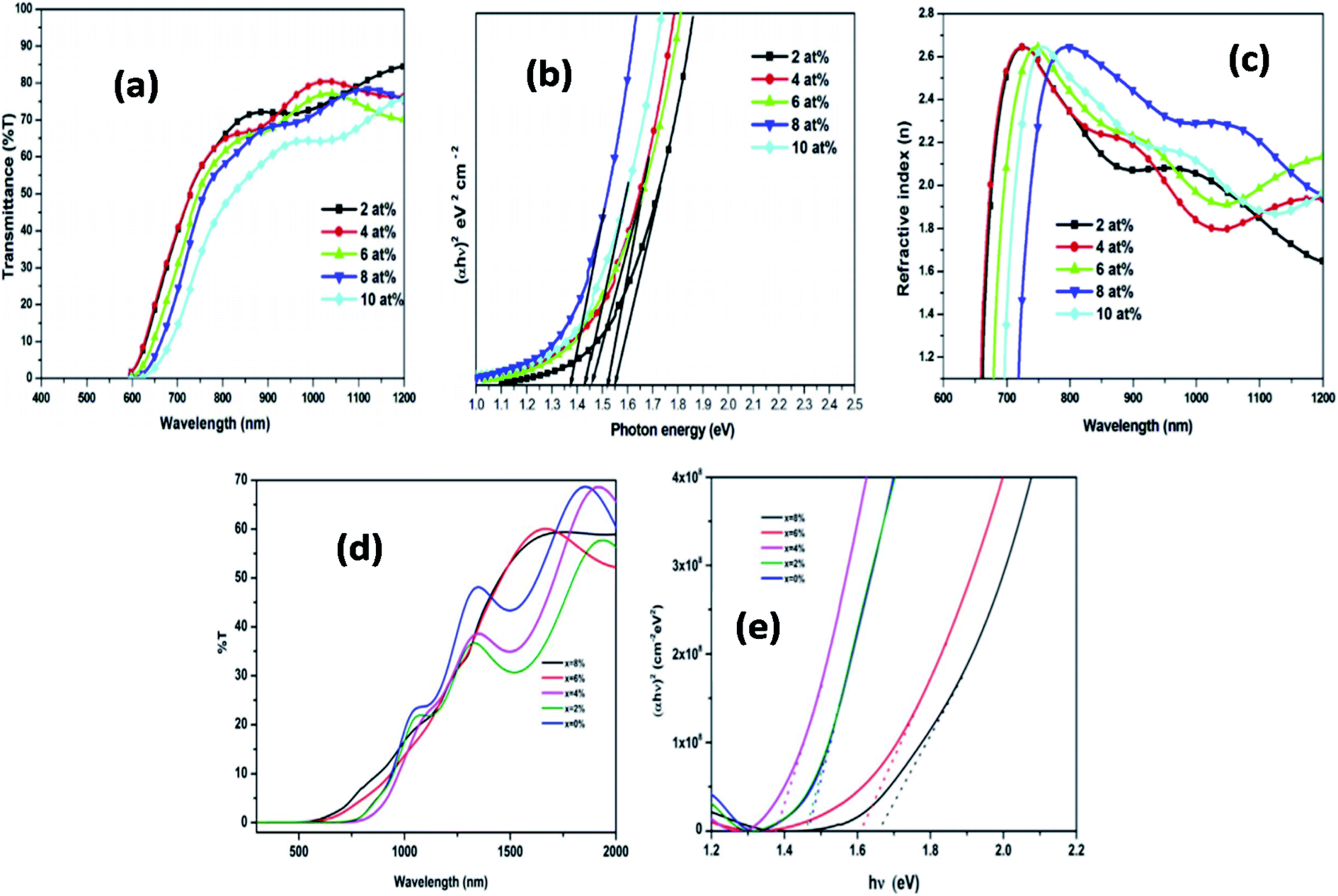 | ||
| Fig. 7 (a) Transmittance spectra (b) plots of (αhν)2 versus hν and (c) variation of refractive index Cu doped SnS thin films prepared at various doping concentrations.58 (d) Transmittance spectra of pure and Cu doped SnS thin films prepared by sol–gel method, (e) plots of (αhν)2 versus hν of pure and Cu doped SnS thin films.111 | ||
Copper as a dopant in the CdS system acts as an acceptor, resulting in a change of resistivity, band interval energy variations, photoelectric properties, respectively. The substitution of Cu2+ ions into the Cd–S lattice was confirmed through variation in lattice parameters, FTIR and PL spectra. The ambient temperature PL spectra demonstrated the existence of two distinct and strong bands such as 408 nm (blue band) and 547 nm (green band), respectively. These bands shifted to a higher wavelength with increased intensity due to Cu doping and reached maximum intensity at Cd0.96Cu0.04S thin film. The appearance and shifting were due to the radiative recombination of holes and electrons via the surface/defect states present and showed great potential for nano-scaled optoelectronic intensive light emitters.109 Thin films of Cu doped ZnS thin films were synthesized by chemical bath deposition technique showed slight shifting with the appearance of three emission peaks at 390 nm, 480 nm and 525 nm. With the increase in Cu concentration, the peak position shifted to higher wavelength and reached maximum intensity for 0.01 M%. The observed enhancement in blue and green light emission was seven and twenty-five-fold greater than undoped film. Optical absorption showed enhancement in bandgap form ZnS to Cu: ZnS film, favoring quantum confinement effect in the developed nanoparticle of size below the Bohr diameter.113 Similarly, the blue shifting observed in both blue (413 to 407 nm) and green band (from 538 to 523 nm) in PL spectra with enhanced intensity confirmed the doping impact of Cu in Cd–Zn–S lattice. This behavior primarily contributed to an increase in particle thickness and size. The observed emission band were attributed to the combined effect of quantisation and defect states due to the imperfection in weakly crystalline lattice structure due to different element sizes of Cu, Cd, and Zn.114
3. Applications
Chalcogenide materials can transmit radiation over wavelengths more significant than 2 μm. These glasses have optical properties that are more significant than that of oxide-based silica glasses. An appropriate amount of doping easily modifies their compositional properties to enhance their efficiency, capability, etc., making them more promising for several optical device applications. Chalcogenide-based thin films are the most famously known candidates for their wide applications in photonics and device applications over the range of 0.6 μm to 15 μm. Their wide range of applications for passive devices like lenses, windows, optical fibers, etc., and active devices like laser fibers, nonlinear devices, etc., makes them more attractive.115–151The doping of suitable metals in the composition of chalcogenide glasses leads to desired structural and optical changes, making them suitable for several applications. When the chalcogenide system is subjected to external stimuli like photo-induced or thermally induced with a sufficiently high electric field, it shows un-stability after a certain point which gives rise to switching patterns.116 This property of chalcogenide glasses depends on electrical conductivity, crystallization capability, chemical ordering, etc. The incorporation of Cu in the Ge–Te thin-film system results in attaining the high resistance state by applying a suitable current pulse which is helpful for the production of switching-based devices.117,118 Cu and Ag possess the properties of good conductivity, so this makes sense that introducing Cu and Ag in the Ge–Te system causes a decrease in the switching field, which is related to the threshold voltage for switching. The performance shown by changing field for both Cu–Ge–Te and Ag–Ge–Te systems is comparable with the same for the composition As–Te system. The incorporation of Cu and Ag in the Ge–Te system shows a lower switching field than that of the As and Se incorporated Ge–Te system.117–121 Introduction of Cu in As30CuxSe70−x shows memory switching property for the composition x < 15; for x > 15 composition shows behavior from high conducting state (ON) to low conduction state (OFF).121,122 Bi doping in GeTe nanowire enhanced the switching mechanism and increased the crystalline and amorphous state resistance, making these thin films suitable for data storage and phase switching applications.123
As excellent transmittance over a vast region, these doped chalcogenide materials are promising sensing devices. The most necessary characteristics for a chemical sensor are potential stability, sensitivity, lifetime, compositional limits, etc. The ion-selective sensor based on chalcogenide possesses good thermal stability and sensitivity during continuous measurements.124 The specific composition of doping Cu and Cd in chalcogenide glasses produces a suitable chalcogenide-based sensor that can be used for chemical purification in industrial work stations.125
Resistance switching-based nonvolatile memory devices, which are also known for resistance random access memory (RRAM), have taken all attention due to their favorable characteristics like low fabrication cost, fast writing, and reading facility, less threshold voltage, and less power consumption, etc.126,127 Phase change memory application mostly depends on the rapid, reversible phase transformations between amorphous and crystalline states, which take place in nano-volume of material under low energy external fluences. Materials of the GeTe–Sb2Te3 pseudo-binary line in particular Ge2Sb2Te5, are considered to be the most promising materials for application in phase change memories. Doping and modification of the structural matrix by the incorporated dopants were deemed to be one of the effective methods for tailoring the properties of semiconductor materials. Thus, for the proper alteration of the electrical and optical properties in PCM materials, alloying is the way that provides a positive gateway to achieve the desired properties of amorphous and crystalline phases of GST. Doping bismuth in Ge2Sb2Te5 significantly changes thermal, optical, and electrophysical characteristics. The influence of bismuth on the electrical and physical properties, charge carrier transport, and nonlinear current–voltage (I–V) characteristics in thin films are beneficial for PCM applications. The most apparent modification of optical properties, current–voltage characteristics, and parameters of the thin films was established for Ge2Sb2Te5 with Bi doping. Thus, doping of Bi in the Ge2Sb2Te5 matrix showed an expansion over the range of material properties, which is essential for the optimization of PCM technology.128 R. Soni has discussed the Cu doped Ge–Se chalcogenide system based on random telegraph noise (RTN) to be used for the RRAM device application. It shows the fluctuation properties depend on the device's programmed resistance, which concludes that the fluctuation is highly sensitive towards the resistance.129 Similarly, the dissolution of Ag in the GexSe1−x system gives rise to a ternary layer that combines the Ag2Se conducting phase and Ge–Se highly-resistive phase. This shows similar characteristics to the Cu doped Ge–Se system as they both possess comparable compositions.130
Electrochemical electrodes having good sensitivity have been developed from Ag-doped chalcogenide glasses and thin films. Considering composition Ag–AsS2 and Ag–GeS2 possess appropriate properties like good ionic conductivity and stability over-acidic solutions, which can be used for sensors.131 A successful investigation has been done on Cu and Ag-doped Ge-based chalcogenide, which acts as an electrolyte in the active medium of a programmable metallization cell (PMC) and proves as the promising candidate for the RRAM application.132 Fick et al. Investigated the thermal diffusion of Ag in the chalcogenide system that proves to be useful for applying the optical waveguides.133 PMC random access memory is dependent on the electrochemical growth and the removal of non-metallic pathways in thin films of the solid electrolyte. The new programmable metallization cell RAM uses metallic Ag-doped amorphous chalcogenide Ge25Se75, and Ge30Se70 thin films considered the next generation of nonvolatile memory application. As a result, this technology enables data storage in Ag-based chalcogenide thin films as a memory storage device. These devices have excellent switching features for PMC-RAM, which promises to be non-volatile, low power, and potentially low cost for the next generation of non-volatile memory applications.134
The introduction of Ag in Ge rich chalcogenide thin films alters the sequence of the local atomic structure. The experimental analysis explained the loss of medium-range order and change in the diffraction curve. According to the structural model, these modifications have a great connection with the application for fast switching memory devices.135 Ag-doped chalcogenide systems are promising candidates for holography and optical memory device applications. Photo-inducing techniques can improve the sensitivity of the materials. For fiber fabrication, incorporating metals in chalcogenide materials increases efficiency due to their exciting properties like low phonon energy and high refractive index. The radiation-induced effect in the chalcogenide system-induced structural reorganization contributing towards silver diffusion. The increase in the structural development occurring inside the films containing 45.5 at% Ge in respect to increasing radiation dose results in an increase in the edge/corner-sharing ratio and allows the diffusion of Ag inside the system. The electrical performance of the device fabricated from the studied films showed a decrease in resistance after irradiation. This is primarily attributed to incorporated Ag diffusion as a consequence of radiation-induced, which characterizes the sensor operation and demonstrated decreased device resistance as a result of the radiation.136
Metals doped chalcogenide glasses are the potential candidates for application in lasing, modulators, ultra-fast telecommunication, optical signal processing, etc.137–140 The introduction of Cu into thin film Cd–S affects the photographic response, making them useful for photovoltaic applications. A higher concentration of impurity Cu will enhance the p-type electrical conductivity of Cd–S.140 Similarly, the introduction of Cu enhances transparency and decreases resistivity, so these modified properties of the system make them appropriate for photovoltaic application.141 Chalcogenide photoresists are widely used in the field of micro as well as optoelectronic devices. Ag-doped in As2S3 film is used to fabricate strongly nonlinear chalcogenide photoresists, and useful for massless photolithography.142 Application-based nanometer dimension pattern lines have been developed through doping Ag in chalcogenide materials. The structure of these Ag-doped lines is similar to that of the accelerating voltage beam parameters.143
Various kinds of third-order nonlinear optical materials have also been characterized and analyzed for their suitability of use in all-optical switching, pulse compression, fiber grating. Among those applications, glass fibers offer the advantage of reduced operating power because of the long interaction length. Because of low losses, silica fibers have been studied in-depth, but their nonlinearity is low and requires very long fibers for communication (>100 m). Third harmonic generation measurements revealed that chalcogenide thin films possessed two orders of magnitude higher nonlinearity than that of silica. A very efficient optical Kerr effect in As2S3 based fibers has been observed, and efficient all-optical switching using small core fiber only few meters long has been demonstrated.144,145 The enhancement of third-order nonlinear effects has been achieved by doping suitable metal in chalcogenide films. For example, solid and nonlinear characteristics of the configuration Ag (paint)–As2Se3–Cu showed challenging behavior. The nonlinear element based on heterojunction Ag–As2Se3–Cu exhibits different conduction behavior in direct and reverse polarization. This strong nonlinearity makes the material more potential for application as a rectifier and dynamical switching devices by using two conduction states. Similarly, 4 at% Cu doped and Ag-doped As2Se3 films for pulse durations on the order of nanoseconds at 1.064 μm.146
A. Kovalskly and his colleagues demonstrated the advantages and application of chalcogenide thin-film photoresists for greyscale lithography. It has been observed that the performance shown by those films could be used to make high-resolution greyscale lithography for IR optics. Application of silver photo dissolution in lithography for microelectromechanical systems applications was also demonstrated.147 Similarly, elaborated analysis on As–S–Se films as recording media for holography and lithography has been presented by J. Teteris. Higher value in the photoinduced refractive index modifications enables the holographic recording with high diffraction efficiency.148 An equivalent As2S3–Ag–(PVDF-TrFE) pyroelectric detector showed a resonant absorption coefficient of 80% and responsivity of 1.4 mV mW−1 that would be beneficial for sensors, imaging and spectroscopy.149 L. Wei presented a low-cost, large-scale nanofabrication approach by combining the lithography imprinting and silver doping to produce a pattern on chalcogenide As2S3 glasses for IR devices. This approach could be used for nanoimprint lithography tools such as Canon's S-FIL and EVG's Smart NIL systems by simply coating a thin Ag layer on a template and using chalcogenide as the imprint resist.150 The surface plasmon polariton excitation effect at the silver–chalcogenide interface due to photostimulated diffusion significantly enhanced the photosensitivity of the structure. In this two-layer Ag–As2S3 structure deposited on the diffraction grating with 899 nm patterns using interference photolithography.151
4. Conclusion
Doping always provides the gateway to unveil several mechanisms and characteristics properties inside the material system. Thus, metal doping in chalcogenide materials attracts much interest due to their wide application in several fields of physics. Through by understanding their several chemical and physical properties and doing some modifications that need, several progressed devices can also be manufactured. There are many more aspects of their properties, stability, and much more things that remain to be investigated. There are signs of progress that have to make by increasing their capability, efficiency which can be achieved by knowing all properties of these chalcogenide thin films. By developing interesting equipment like lasers, optical sensors, amplifiers, etc. which will help to improve in the several sectors of science and technologies.Conflicts of interest
There are no conflicts of interests.References
- M. Frumar and T. Wagner, Ag-doped chalcogenide glasses and their applications, Curr. Opin. Solid State Mater. Sci., 2003, 7, 117–126 CrossRef CAS.
- B. Bureau, X. H. Zhang, F. Smektala, J. Adam, J. Lucas, J. Troles, H. Ma, C. B. Pledel, P. Lucas, D. Le-Coq, M. R. Riley and J. H. Simmons, Recent advances in chalcogenide glasses, J. Non-Cryst. Solids, 2004, 345–346, 276–283 CrossRef.
- M. Frumar, J. Jedelsky, B. Frumarov, T. Wagner and M. Hrdlicka, Optically and thermally induced changes of structure, linear and nonlinear optical properties of chalcogenides thin films, J. Non-Cryst. Solids, 2003, 326–327, 399–404 CrossRef.
- M. M. Hafiz, A. A. Othman, M. M. Elnahass and A. T. Al-Motasem, Composition and electric field effects on the transport properties of Bi doped chalcogenide glasses thin films, Physica B, 2007, 390, 286–292 CrossRef CAS.
- M. Kastner, D. Adler and H. Fritzsche, Valence alteration model for localized gap states in lone pair semiconductors, Phys. Rev. Lett., 1976, 37, 1504–1507 CrossRef CAS.
- A. M. Andriesh and M. S. Iovu, Optical properties of chalcogenide glasses, Moldavian J. Phys. Sci., 2003, 2, 3–4 Search PubMed.
- N. F. Mott, The increase in the conductivity of chalcogenide glasses by the addition of certain impurities, Philos. Mag., 1976, 34, 1101–1108 CrossRef CAS.
- N. Tohge, T. Minami, Y. Yamamoto and M. Tanaka, Electrical and optical properties of n-type semiconducting chalcogenide glasses in the system Ge-Bi-Se, J. Appl. Phys., 1980, 51, 1048–1053 CrossRef CAS.
- K. L. Bhatia, G. Parthasarthy, A. Sharma and E. S. R. Gopal, Carrier sign reversal in Bi-doped bulk amorphous semiconductors Ge20Te80−xBix, Phys. Rev. B: Condens. Matter Mater. Phys., 1988, 38, 6342–6344 CrossRef CAS PubMed.
- P. Sharma, M. S. El-Bana, S. S. Fouad and V. Shrama, Effect of compositional dependence on physical and optical parameters of Te17Se83−xBix glassy system, J. Alloys Compd., 2016, 667, 204–210 CrossRef CAS.
- P. K. Sahu and R. Das, Influence of trivalent bismuth doping on optoelectronic and microstructural properties of hydrophilic nanocrystalline cadmium selenide thin films, Thin Solid Films, 2020, 693, 137675 CrossRef CAS.
- N. F. Mott, Metallic and non-metallic behavior in compounds of transition metals, Phil. Mag., 1969, 20, 1–21 CrossRef CAS.
- A. Feltz, Amorphous inorganic materials and glasses, VCH, Germany, 1993 Search PubMed.
- D. Lezal, Chalcogenide glasses- survey and progress, J. Optoelectron. Adv. Mater., 2003, 5, 23–34 CAS.
- A. Gubanova, T. Krysskov, A. Paiuk and R. Laiho, Some magnetic properties of chalcogenide glasses As2S3 and As2Se3 doped with Cr, Mn, and Yb, Moldavian J. Phys. Sci., 2009, 8, 178–185 Search PubMed.
- R. M. Mehra, N-type conduction in Pb doped Se-In chalcogenide Se-In chalcogenide glasses, J. Appl. Phys., 1997, 81, 7842–7844 CrossRef CAS.
- J. M. Harbold, F. O. Ilday, F. W. Wise, J. S. Sanghera, V. Q. Nguyen, L. B. Shaw and I. D. Aggarwal, Highly nonlinear As-S-Se glasses for all optical switching, Opt. Lett., 2002, 27, 119–121 CrossRef CAS PubMed.
- M. Shkir, Z. R. Khan, M. Anis, S. S. Shaikj and S. AlFaify, A comprehensive study of opto-electrical and nonlinear properties of Cu-CdS thin films for optoelectronics, Chin. J. Phys., 2020, 63, 51–62 CrossRef CAS.
- M. S. El-Bana and S. S. Fouad, Optoelectrical properties of Ge10Se90 and Ge10Se85Cu5 thin films illuminated by laser beams, Appl. Phys. A, 2018, 132, 124 Search PubMed.
- E. Mytilineou, Chalcogenide amorphous semiconductors- chemical modification or doping, J. Optoelectron. Adv. Mater., 2002, 4, 705–710 CAS.
- Q. Yin and L. Chen, Enhanced optical properties of Sn-doped Ge2Sb2Te5 thin film with structural evolution, J. Alloys Compd., 2019, 770, 692–700 CrossRef CAS.
- J. Kaur and S. K. Tripathi, Annealing-induced optical and sub-band-gap absorption parameters of Sn-doped CdSe thin films, Philos. Mag., 2016, 96, 45–57 CrossRef CAS.
- M. Fadel, K. Sadeek and N. A. Hegab, Effect of Sn content on the electrical and optical properties of Ge1−xSnxSe3 glasses, Vacuum, 2000, 57, 307–317 CrossRef CAS.
- S. Kumar, D. Singh and R. Thangaraj, Electronic structure and optical bandgap of silver photo diffused Ge2Sb2Te5 thin film, Appl. Surf. Sci., 2013, 273, 437–443 CrossRef CAS.
- N. Kunda, A. Thakur, F. Singh and A. P. Singh, Effect of ion irradiation on the optical properties of Ag-doped Ge2Sb2Te5 (GST) thin films, Nucl. Instrum. Methods Phys. Res., Sect. B, 2020, 467, 40–43 CrossRef.
- K. Tanaka and K. Shimakawa, Amorphous Chalcogenide Semiconductors and Related Materials, Springer Publication, 2011, pp. 63–84 Search PubMed.
- M. S. Iovu, S. D. Shutov, A. M. Andriesh, E. I. Kamitos and C. P. Varsamis, Spectroscopic studies of bulk As2Se3 glasses and amorphous films doped with Dy, Sm, and Mn, J. Optoelectron. Adv. Mater., 2001, 3, 443–454 CAS.
- V. Trnovcova, I. Furar and D. Lezal, Influence of doping on physical properties of vitreous As2Se3, J. Non-Cryst. Solids, 2007, 353, 13–15 CrossRef.
- I. Sharma, P. Kumar and S. K. Tripathi, Physical and optical properties of bulk and thin films of a–Ge–Sb–Te lone-pair semiconductors, Phase Transitions, 2017, 90, 653–671 CrossRef CAS.
- A. S. Hassanien, I. Sharma and A. A. Akl, Physical and optical properties of a-Ge-Sb-Se-Te bulk and film samples: Refractive index and its association with electronic polarizability of thermally evaporated a-Ge15−xSbxSe50Te35 thin-films, J. Non-Cryst. Solids, 2020, 531, 119853 CrossRef CAS.
- S. Yoo, C. Yoo, E. S. Park, W. Kim, Y. K. Lee and C. S. Hwang, Chemical interactions in the atomic layer deposition of Ge–Sb–Se–Te films and their ovonic threshold switching behavior, J. Mater. Chem. C, 2018, 6, 5025–5032 RSC.
- M. F. Churbanov, I. V. Scripachev, G. E. Snopatin, V. S. Shiryaev and V. G. Plotnichenko, High-purity glasses based on arsenic chalcogenides, J. Optoelectron. Adv. Mater., 2001, 3, 341 CAS.
- N. F. Mott and E. A. Davis, Electronic processes in non-crystalline solids, Clarendon, Oxford, 1979, p. 428 Search PubMed.
- D. Lezal, J. Pedlikova and J. Zavadil, Chalcogenide glasses for optical and photonics applications, J. Optoelectron. Adv. Mater., 2004, 6, 133–137 CAS.
- R. A. Street and N. F. Mott, States in the gap in glassy semiconductors, Phys. Rev. Lett., 1975, 35, 1293–1296 CrossRef CAS.
- N. Tohge, Y. Yamamoto, T. Minami and M. Tanaka, Preparation of n-type semiconducting Ge20Bi10Se70 glass, Appl. Phys. Lett., 1979, 34, 640–641 CrossRef CAS.
- N. Tohge, T. Minami and M. Tanaka, Photoconductivity of vitreous chalcogenides chemically modified by bismuth, J. Non-Cryst. Solids, 1983, 59–60, 999–1002 CrossRef CAS.
- A. Aparimita, M. Behera, C. Sripan, R. Ganesan, S. Jena and R. Naik, Effect of Bi addition on the optical properties of Ge30Se70−xBix thin films, J. Alloys Compd., 2018, 739, 997–1004 CrossRef CAS.
- M. Behera, R. Naik, C. Sripan, R. Ganesan and N. C. Mishra, Influence of Bi content on linear and nonlinear optical properties of As40Se60−xBix chalcogenide thin films, Curr. Appl. Phys., 2019, 19, 884–893 CrossRef.
- A. El-Korashy, N. El-Kabany and H. El-Zahed, Optical, electrical and the related parameters of amorphous Ge–Bi–Se thin films, Phys. B, 2005, 365, 55–64 CrossRef CAS.
- H. El-Zahed and A. El-Korashy, Influence of composition on the electrical and optical properties of Ge20BixSe80−x films, Thin Solid Films, 2000, 376, 236–240 CrossRef CAS.
- M. M. El-Samanoudy, Effect of composition and deposition parameters on optical properties of Ge25Sb15− xBixS60 thin films, Thin Solid Films, 2003, 423, 201–211 CrossRef CAS.
- S. Sharma, P. Kumar and R. Thangaraj, Effect of Bi additive on structure and optical properties of amorphous BixIn25−xSe75 chalcogenide films, Curr. Appl. Phys., 2013, 13, 731–735 CrossRef.
- P. Sharma, M. Vashistha and I. P. Jain, Optical properties of Ge20Se80−XBiX thin films, J. Opto-Electron. Adv. Mater., 2005, 7, 2647–2654 CAS.
- A. Sharma and P. B. Barman, Effect of Bi incorporation on the glass transition kinetics of Se85Te15 glassy alloy, J. Therm. Anal. Calorim., 2009, 96, 413–417 CrossRef CAS.
- R. Naik, R. Ganesan and K. S. Sangunni, Optical properties change with the addition and diffusion of Bi to As2S3 in the Bi/As2S3 bilayer thin film, J. Alloy Compd., 2013, 554, 293–298 CrossRef CAS.
- A. Aparimita, C. Sripan, R. Ganesan and R. Naik, Photo and thermal-induced Bi2Se3 formation from Bi/GeSe2 heterojunction layer for topological insulator, Opt. Mater., 2019, 89, 157–163 CrossRef CAS.
- P. Priyadarshini, D. Sahoo, D. Alagarasan, S. Varadharajaperumal and R. Naik, Structural and optoelectronic properties change in Bi/In2Se3 heterostructure films by thermal annealing and laser irradiation, J. Appl. Phys., 2021, 129, 223101 CrossRef CAS.
- A. A. Al-Ghamdi, S. A. Khan, S. Al-Heniti, F. A. Al-Agel, F. Al-Harbi and M. Zulfequar, Effects of laser irradiation on optical properties of amorphous and annealed Ga15Se81In4 and Ga15Se79In6 chalcogenide thin films, J. Alloys Compd., 2010, 505, 229–234 CrossRef CAS.
- M. A. M. Khan, M. Zulfequar and M. Husain, Optical investigation of a-Se100−xBix alloys, Opt. Mater., 2003, 22, 21–29 CrossRef.
- P. Yadav and A. Sharma, Investigation of optical nonlinearities in Bi-doped Se-Te chalcogenide thin films, J. Elect. M., 2015, 44, 916–921 CrossRef CAS.
- V. Takats, I. Vojnarovich, V. Pinzenik, I. Mojzes, S. Kokenyesi and K. S. Sangunni, Stimulated changes in Bi (Sb)/As2S3 nanolayered structures, J. Phys. Chem. Solids, 2007, 68, 943–947 CrossRef CAS.
- E. Marquez, J. M. Gonzalez-Leal, A. M. Bernal-Oliva, R. J. Garay and T. Wagnerb, Optical properties of amorphous (As0. 33S0. 67)100−xTex (x= 0, 1, 5 and 10) chalcogenide thin films, photodoped step-by-step with silver, J. Non-Cryst. Solids, 2008, 354, 503–508 CrossRef CAS.
- D. Lezal, Chalcogenide glasses-survey and progress, J. Optoelectron. Adv. Mater., 2003, 5, 23–34 CAS.
- R. Naik, P. P. Sahoo, C. Sripan and R. Ganesan, Laser-induced Bi diffusion in As40S60 thin films and the optical properties change probed by FTIR and XPS, Opt. Mater., 2016, 62, 211–218 CrossRef CAS.
- A. Kennedy, V. S. Kumar and K. P. Raj, Influence of substrate temperature on structural, morphological, optical and electrical properties of Bi-doped MnInS4 thin films prepared by nebuliser spray pyrolysis technique, J. Phys. Chem. Solids, 2017, 110, 100–107 CrossRef CAS.
- D. C. Priya, T. Daniel, J. Henry, K. Mohanraj, G. Sivakumar, S. Thanikaikarasan and P. J. Sebastian, Thermally deposited Sb2S3: Bi thin films for solar cell absorber, J. New Mater. Electrochem. Syst., 2018, 21, 037–042 CrossRef CAS.
- R. Das and R. Kumar, Structural, photoluminescence and optical properties of chemically deposited (Cd1−xBix)S thin films as a function of dopant concentration, J. Mat. Sci. Mat. Electron., 2013, 24, 697–703 CrossRef CAS.
- A. S. Hassanien and I. Sharma, Band-gap engineering, conduction and valence band positions of thermally evaporated amorphous Ge15−xSbx Se50 Te35 thin films: Influences of Sb upon some optical characterizations and physical parameters, J. Alloys Compd., 2019, 798, 750–763 CrossRef CAS.
- D. C. Sati, A. Dahshan and P. Sharma, Photoinduced effects for amorphous chalcogenide semiconductors, Appl. Mater. Today, 2019, 17, 142–158 CrossRef.
- A. S. Hassanien and I. Sharma, Optical properties of quaternary a-Ge15−xSbxSe50Te35 thermally evaporated thin-films: refractive index dispersion and single oscillator parameters, Optik, 2020, 200, 163415 CrossRef CAS.
- S. Vallem, K. V. Bangera and G. K. Shivakumar, Enhanced thermoelectric power of Al and Sb doped In2Te3 thin films, Mat. Sci. Semicond. Proc., 2019, 93, 366–370 CrossRef CAS.
- Z. Y. Zhang, F. Chen, S. B. Lu, Y. H. Wang, X. Shen, S. X. Dai and Q. H. Nie, Linear and nonlinear optical properties of Sb-doped GeSe2 thin films, Chin. Phys. B, 2015, 24, 066801 CrossRef.
- F. A. Al-Agel, Structural and optical properties of thermally evaporated Sb doped Ge–Se thin films, Opt. Laser Technol., 2013, 54, 208–213 CrossRef CAS.
- P. Kumar, J. Kaur, S. K. Tripathi and I. Sharma, Effect of antimony (Sb) addition on the linear and nonlinear optical properties of amorphous Ge–Te–Sb thin films, Indian J. Phys., 2017, 91, 1503–1511 CrossRef CAS.
- S. Mishra, P. Lohia and D. K. Dwivedi, Structural and optical properties of (Ge11.5 Se67.5 Te12.5)100−x Sbx (0 ≤ x ≤ 30) chalcogenide glasses: A material for IR devices, Infrared Phys. Technol., 2019, 100, 109–116 CrossRef CAS.
- P. Pradhan, R. Naik, N. Das and A. K. Panda, Laser induced optical properties change by photo diffusion of Sb into As2Se3 chalcogenide thin films, Opt. Laser Technol., 2017, 96, 158–165 CrossRef CAS.
- R. Naik, R. Ganesan and K. S. Sangunni, Compositional dependence on the optical properties of amorphous As2 − xS3 − xSbx thin films, Thin Solid Films, 2010, 518, 5437–5441 CrossRef CAS.
- R. Naik, A. Jain, R. Ganesan and K. S. Sangunni, Compositional dependence optical properties study of As40Se60 − xSbx thin films, Thin Solid Films, 2012, 520, 2510–2513 CrossRef CAS.
- R. Naik and R. Ganesan, Effect of compositional variations on the optical properties of SbxSe60 −xS40 thin films, Thin Solid Films, 2015, 579, 95–102 CrossRef CAS.
- E. R. Shaaban, M. A. Kaid, E. S. Moustafa and A. Adel, Effect of compositional variations on the optical properties of Sb–Ge–Se thin films, J. Phys. D: Appl. Phys., 2008, 41, 125301 CrossRef.
- N. S. Patil, A. M. Sargar, S. R. Mane and P. N. Bhosale, Growth mechanism and characterisation of chemically grown Sb doped Bi2Se3 thin films, Appl. Surf. Sci., 2008, 254, 5261–5265 CrossRef CAS.
- M. Ali, W. A. A. Syed, M. Zubair, N. A. Shah and A. Mehmood, Physical properties of Sb-doped CdSe thin films by thermal evaporation method, Appl. Surf. Sci., 2013, 284, 482–488 CrossRef CAS.
- S. Mathuri, K. Ramamurthi and R. R. Babu, Effect of Sb incorporation on the structural, optical, morphological and electrical properties of CdSe thin films deposited by electron beam evaporation technique, Thin Solid Films, 2018, 660, 23–30 CrossRef CAS.
- N. Suriyanarayanan and C. Mahendran, Effect of temperature on structural, optical and photoluminescence properties of antimony (Sb) doped polycrystalline CuInS2 thin films prepared by spray pyrolysis, Mater. Sci. Eng., 2011, 176, 417–424 CrossRef CAS.
- M. Kawasaki, J. Kawamura, Y. Nakamura and M. Aniya, Ionic conductivity of Agx (GeSe3)1−x (0≤ x ≤ 0.571) glasses, Solid State Ionics, 1999, 123, 259–269 CrossRef CAS.
- M. Ribes, E. Bychkov and A. Pradel, Ion transport in chalcogenide glasses: dynamics and structural studies, J. Optoelectron. Adv. Mater., 2001, 3, 665–674 CAS.
- R. Belin, G. Taillades, A. Pradel and M. Ribes, Ion dynamics in superionic chalcogenide glasses: complete conductivity spectra, Solid State Ionics, 2000, 136–137, 1025–1029 CrossRef CAS.
- I. Shimizu, H. Sakuma, H. Kokado and E. Inoue, The photo-erasable memory switching effect of Ag photo-doped chalcogenide glasses, B. Chem. Soc. Jpn., 1973, 46, 3662–3665 CrossRef CAS.
- K. Ogusu, S. Maeda, M. Kitao, H. Li and M. Minakata, Optical and structural properties of Ag(Cu)–As2Se3 chalcogenide films prepared by a photodoping, J. Non-Cryst. Solids, 2004, 347, 159–165 CrossRef CAS.
- A. Zakery and S. R. Elliott, Optical properties and application of chalcogenide glasses - a review, J. Non-Cryst. Solids, 2003, 330, 1–12 CrossRef CAS.
- E. Shahriari, Z. M. Farsani, M. G. Varnamkhasti and R. Zamiri, Linear and nonlinear optical properties of Ag-doped Zn-S thin film, Opt. Quant. Electron., 2017, 49, 151–163 CrossRef.
- R. Naik, A. Aparimita, D. Alagarasan, S. Varadharajaperumal and R. Ganesan, Linear and nonlinear optical properties change in Ag/GeS heterostructure thin films by thermal annealing and laser irradiation, Opt. Quant. Electron., 2020, 52, 136 CrossRef CAS.
- M. Shkir, S. S. Shaikh and S. Al-Faify, An investigation on optical nonlinear and optical limiting properties of Cd-S: an effect of Te doping concentrations for optoelectronic applications, J. Mater. Sci. Mater. Elect., 2019, 30, 17469–17480 CrossRef CAS.
- T. Wagner, S. Schroeter, T. Glaser and M. Vlcek, Holographic grating preparation in Ag/As30S70 multilayer and bilayer structures, J. Non-Cryst. Solids, 2003, 326–327, 500–504 CrossRef.
- R. Naik, A. Aparimita, C. Sripan and R. Ganesan, Structural, linear and nonlinear optical properties of annealed and irradiated Ag/Se heterostructure films for optoelectronic applications, Optik, 2019, 194, 162894 CrossRef CAS.
- A. Viswanathan and S. Thomas, Tunable linear and nonlinear optical properties of Ge-Se-Sb chalcogenide glass with solute concentration and with silver doping, J. Alloy. Compd., 2019, 798, 424–430 CrossRef CAS.
- K. H. Song, S. W. Kim, J. H. Seo and H. Y. Lee, Characteristics of amorphous Ag0.1(Ge2Sb2Te5)0.9 thin film and its ultrafast crystallization, J. Appl. Phys., 2008, 104, 103516 CrossRef.
- P. Singh, R. Kaur, P. Sharma, V. Sharma, M. Mishra, G. Gupta and A. Thakur, Optical bandgap tuning of Ag doped Ge2Sb2Te5 thin films, J. Mater. Sci.-Mater. El., 2017, 28, 11300–11305 CrossRef CAS.
- P. Singh, P. Sharma, V. Sharma and A. Thakur, Linear and nonlinear optical properties of Ag-doped Ge2Sb2Te5 thin films estimated by single transmission spectra, Semicond. Sci. Tech., 2017, 32, 045015 CrossRef.
- B. Tiss, Y. Moualhi, N. Bouguila, M. Erouel, M. Kraini, S. ALaya, S. Aouida, C. V. Vazquez, C. Moura and L. Cunha, Influence of silver doping on physical properties of sprayed In2S3 films for solar cells application, J. Mater. Sci. Mat. Elect., 2021, 32, 4568–4580 CrossRef CAS.
- Y. Chen, J. min, Q. Wang and S. Li, Metal sulfide precursor aqueous solutions for fabrication of Ag-doped ZnxCd1−xS quantum dots thin films, J. Lumin., 2016, 180, 258–263 CrossRef CAS.
- A. Andrish, M. Iovu, S. Shutov, M. Bulgaru, E. Colomeyco, S. Malcov, V. Verlan, M. Popescu, F. Tudorica, M. Leonovici, V. Mihai and M. Steflea, Atomic structure and electronic transport properties of glassy As2Se3 doped with Sn, Mn, Dy and Sm, Optoelectronics, 1996, 4, 14 Search PubMed.
- M. S. Iovu, S. D. Shutov, P. Boolchand, D. G. Georgiev and E. P. Colomeico, The relaxation of photodarkening in Sn doped amorphous As2Se3 films, J. Optoelectron. Adv. Mater., 2003, 5, 389–395 CAS.
- P. K. Sahu, R. Das and R. Lalwani, Incorporation of tin in nanocrystalline CdSe thin films: a detailed study of optoelectronic and microstructural properties, Appl. Phys. A, 2018, 124, 665 CrossRef.
- P. Yadav and A. Sharma, Refractometric studies of Sn doped Se-Te-Bi Chalcogenide glasses, Technol. Lett., 2014, 1, 17–20 Search PubMed.
- G. Singh, A. Kaura, M. Mukul and S. K. Tripathi, Electrical, optical, and thermal properties of Sn-doped phase change material Ge2Sb2Te5, J. Mater. Sci., 2013, 48, 299–303 CrossRef CAS.
- V. Bilovol, M. Fontana, J. A. Rocca, H. H. Medina Chanduvi, A. M. Mudarra Navarro, A. V. Gil Rebaza, L. A. Errico, A. Liang, D. Errandonea and A. M. Urena, Structural, vibrational and electronic properties in the glass crystal transition of thin films Sb70Te30 doped with Sn, J. Alloys Compd., 2020, 845, 156307 CrossRef CAS.
- A. A. A. Darwish, M. Rashad, A. E. Bakheet and M. M. El-Nahass, Linear and nonlinear optical properties of GeS2−xSnx (0 ≤ x ≤ 0.8) thin films for optoelectronic applications, J. Alloy. Compd., 2017, 709, 640–645 CrossRef CAS.
- Z. Zhen-Ying, C. Fen, L. Shun-Bin, W. Yong-Hui, S. Xiang, D. Shi-Xun and N. Qiu-Hua, Linear and nonlinear optical properties of Sb-doped GeSe2 thin films, Chin. Phys. B, 2015, 24(6), 066801 CrossRef.
- F. Asousgi and M. Kanzari, Study of the optical properties of Sn-doped Sb2S3 thin films, Energ. Procedia, 2011, 10, 313–322 CrossRef.
- S. Mushtaq, B. Ismail, M. A. Zeb, N. J. S. Kissinger and A. Zeb, Low-temperature synthesis and characterization of Sn-doped Sb2S3 thin film for solar cell applications, J. Alloys Compd., 2015, 632, 723–728 CrossRef CAS.
- M. Kraini, N. Bouguila, I. Halidou, A. Moadhen, C. V. Vazquez, M. A. L. Quintela and S. Alaya, Study of optical and electrical properties of In2S3:Sn films deposited by spray pyrolysis, J. Electron. Mater., 2015, 44, 2536–2543 CrossRef CAS.
- S. Ebrahimi and B. Yarmand, Solvothermal growth of aligned SnxZn1−xS thin films for tunable and highly response self-powered UV detectors, J. Alloys Compd., 2020, 827, 154246 CrossRef CAS.
- J. Hu, X. Sun, A. M. Agarwal, J. F. Viens and L. C. Kimerling, Studies on structural, electrical, and optical properties of Cu doped As–Se–Te chalcogenide glasses, J. Appl. Phys., 2007, 101, 063520 CrossRef.
- L. Liu, I. W. Chen, F. Q. Huang and L. D. Chen, Improved Thermoelectric Properties of Cu-Doped Quaternary Chalcogenides of Cu2CdSnSe4, Adv. Mater., 2009, 21, 3808–3812 CrossRef.
- C. H. Unnithan, P. Predeep and S. Jayakumar, Doping effect of copper in germanium tellurium semiconducting glass system, J. Phy. Chem. Solids, 2003, 64, 707–709 CrossRef CAS.
- T. Hussain, S. Aslam, F. Mustafa, K. O. Ighodalo and M. A. Ahmad, Study of the extrinsic properties of copper doped cadmium sulfide thin film by hydrothermal assisted CBD method, Mat, Research Exp., 2019, 6, 1–7 Search PubMed.
- M. Muthusamy and S. Muthukumaran, Effect of Cu-doping on structural, optical and photoluminescence properties of CdS thin films, Optik, 2015, 126, 5200–5206 CrossRef CAS.
- F. Gode, Effect of Cu doping on CdS as a multifunctional nanomaterial: Structural, morphological, optical and electrical properties, Optik, 2019, 197, 163217 CrossRef CAS.
- P. R. Bommireddy, C. S. Musalikunta, C. Uppala and S. H. Park, Influence of Cu doping on physical properties of sol-gel processed SnS thin films, Mat. Sci. Semicon. Proc., 2017, 71, 139–144 CrossRef CAS.
- K. S. Kumar, A. G. Manohari, C. Lou, T. Mahalingam and S. Dhanapanian, Influence of Cu dopant on the optical and electrical properties of spray deposited tin sulphide thin films, Vacuum, 2016, 128, 226–229 CrossRef.
- K. Jayanthi, S. Chawla, H. Chander and D. Haranath, Structural, optical and photoluminescence properties of ZnS: Cu nanoparticle thin films as a function of dopant concentration and quantum confinement effect, Cryst. Res. Technol., 2007, 42, 976–982 CrossRef CAS.
- M. Ashokkumar and S. Muthukumaran, Cu doping effect on optical, structural and morphological properties of Cd0.9Zn0.1S thin films, J. Lumin., 2014, 145, 167–174 CrossRef CAS.
- M. F. Chustanov, I. V. Seripachev, V. S. Shiriaev, V. G. Snopin and V. Y. Plotnichenko, High-purity glasses based on arsenic chalcogenides, J. Optoelectron. Adv. Mater., 2001, 3, 341 Search PubMed.
- W. A. Syed, S. Ahmed, M. S. Saleem and N. A. Shah, Cu-doped Zn-Te thin films for potential energy applications, Chalcogenide Lett, 2015, 12, 215–226 CAS.
- K. Ramesh, S. Asokan, K. S. Sangunni and E. S. R. Gopal, Electrical Switching in germanium telluride glasses doped with Cu and Ag, Appl. Phys., 1999, 69, 421–425 CAS.
- K. Ramesh, S. Asokan, K. S. Sangunni and E. S. R. Gopal, Effect of topological thresholds on thermal behaviour of germanium telluride glasses containing metallic additive, Eur. Phys. J. B, 1998, 6, 207–212 CrossRef CAS.
- R. A. Narayanan, A. Kumar and S. Asokan, Evidence concerning the effect of topology on electrical switching in chalcogenide network glasses, Phys. Rev. B: Condens. Matter Mater. Phys., 1996, 54, 4413–4415 CrossRef CAS PubMed.
- S. Murugavel and S. Asokan, Carrier-type reversal in Pb-modified chalcogenide glasses, Phys. Rev. B: Condens. Matter Mater. Phys., 1998, 58, 4449–4453 CrossRef CAS.
- M. M. Haifz, M. M. Ibrahim, M. Dongol and F. H. Hammad, Effect of composition on the structure and electrical properties of As-Se-Cu glasses, J. Appl. Phys., 1983, 54, 1950–1954 CrossRef CAS.
- Y. Asahara and T. Izumitani, Voltage controlled switching in Cu-As-Se compositions, J. Non-Cryst. Solids, 1972, 11, 97–104 CrossRef CAS.
- J. Zhang, R. Huang, L. Shi, L. Wang and F. Wei, Bi doping modulating structure and phase-change properties of GeTe nanowires, Appl. Phys. Lett., 2013, 102, 063104 CrossRef.
- J. Troles and L. Brilland, Chalcogenide microstructured optical fibres for mid-IR applications, C. R. Phys., 2017, 18, 19–23 CrossRef CAS.
- J. L. Adam and X. Zhang, Chalcogenide glasses: preparation, properties and applications, Woodhead Publishing, 2014 Search PubMed.
- Y. Watanabe, Review of resistance switching of ferroelectrics and oxides in quest for unconventional electronic mechanisms, Ferroelectrics, 2007, 349, 190–209 CrossRef CAS.
- R. Waser and M. Aono, Nanoionics-based resistive switching memories, Nat. Mater., 2007, 6, 833–840 CrossRef CAS PubMed.
- H. Ph. Nguyen, S. A. Kozyukhin and A. B. Pevtsov, Influence of bismuth on the optical properties of Ge2Sb2Te5 thin films, Semiconductors, 2014, 48, 577–583 CrossRef CAS.
- R. Soni, P. Meuffels, A. Petraru, M. Weides, C. Kugeler, R. Waser and H. Kohlstedt, Probing Cu doped Ge0.3Se0.7 based resistance switching memory devices with random telegraph noise, J. Appl. Phys., 2010, 107, 024–517 CrossRef.
- M. Mitkova, Y. Wang and P. Boolchand, Dual chemical role of Ag as an additive in chalcogenide glasses, Phys. Rev. Lett., 1999, 83, 3848–3851 CrossRef CAS.
- M. Frumar, Z. Cernosek, J. Jedelsky, B. Frumarova and T. Wagner, Photo-induced changes of structure and properties of amorphous binary and ternary chalcogenides, J. Optoelectron. Adv. Mater., 2001, 3(2), 177–188 CAS.
- M. N. Kozicki, M. Yun, L. Hilt and A. Singh, Applications of programmable resistance changes in metal-doped chalcogenides, Solid State Ionics, 1999, 99, 298–309 Search PubMed.
- J. Fick, B. Nicolas, C. Rivero, K. Elshot, R. Irwin, K. A. Richardson, M. Fischer and R. Vallee, Thermally activated silver diffusion in chalcogenide thin films, Thin Solid Films, 2002, 418, 215–221 CrossRef CAS.
- H. Choi, K. H. Nam, Y. W. Koo and H. B. Chung, Characteristics on electrical resistance change of Ag doped chalcogenide thin film application for programmable metallization cell, J. Electroceram, 2009, 23, 322–325 CrossRef CAS.
- M. Mitkova, Y. Sakaguchi, D. Tenne, S. K. Bhagat and T. L. Alford, Structural details of Ge-rich and silver-doped chalcogenide glasses for nanoionic nonvolatile memory, Phys. Status Solidi A, 2010, 207, 207 CrossRef.
- M. Mitkova, P. Chen, M. Ailavajhala, D. P. Butt, D. A. Tenne, H. Barnaby and I. S. Esqueda, Gamma ray induced structural effects in bare and Ag doped Ge–S thin films for sensor application, J. Non-Cryst. Solids, 2013, 377, 195–199 CrossRef CAS.
- I. Sharma, S. K. Tripathi and P. B. Barman, Effect of deposition parameters and semi-empirical relations between nonlinear refractive index with linear refractive index and third-order susceptibility for a Ge20Se70−xIn10Bix thin films, J. Appl. Phys., 2011, 110, 043108 CrossRef.
- P. Sharma and S. C. Katyal, Linear and nonlinear refractive index of As–Se–Ge and Bi-doped As–Se–Ge thin films, J. Appl. Phys., 2010, 107, 113527 CrossRef.
- I. D. Tolmachov, A. V. Stronski and M. Vlcek, Optical properties and structure of As-Ge-Se thin films, Semicond. Phys., Quantum Electron. Optoelectron., 2010, 13, 276–279 CrossRef CAS.
- D. Petre, I. Pintilie and E. Pentia, T Botila, the influence of Cu doping on optoelectronic properties of chemically deposited Cd-S, Mater. Sci. Eng. B, 1999, 58, 238–243 CrossRef.
- S. J. Gnanamuthu, S. J. Jeyakumar, I. K. Punithavath, P. C. Jobe Prabhakar, M. Suganya, K. Usharani and A. R. Balu, Properties of spray deposited nano needle structured Cu-doped Sn2S3 thin films towards photovoltaic applications, Optik, 2016, 127, 3999–4003 CrossRef CAS.
- V. Lyubin, A. Arsh and M. Klebanov, Nonlinear photoresists for maskless photolithography on the basis of Ag-doped As2S3 glassy films, Appl. Phys. Lett., 2008, 92, 011118 CrossRef.
- K. Mietzsch and A. G. Fitzgerald, Electron beam induced patterning of thin film arsenic-based chalcogenides, Appl. Surf. Sci., 2000, 162–163, 464–468 CrossRef CAS.
- A. Zakery and S. R. Ellott, Optical nonlinearities in chalcogenide glasses and their applications, Springer, Heidelberg, 2007, vol. 135, pp. 107–128 Search PubMed.
- M. Popescu, A. Lorinczi, F. Gherendi, M. Nistor, A. Velea, I. D. Simandan and F. Sava, Nonlinear behaviour in silver – arsenic sulfide system, J. Ovonic Res., 2011, 7, 131–133 CAS.
- K. Ogusu and K. Shinkawa, Optical nonlinearities in As2Se3 chalcogenide glasses doped with Cu and Ag for pulse durations on the order of nanoseconds, Optics Exp, 2009, 17, 8165–8172 CrossRef CAS PubMed.
- P. Kovalskyy, J. Cech, M. Vlcek, C. M. Waits, M. Dubey, W. R. Heffner and H. Jain, Chalcogenide glass e-beam and photoresists for ultrathin grayscale patterning, J. Micro/Nanolithography, MEMS, and MOEMS, 2009, 8, 043012 CrossRef.
- J. Teteris and M. Reinfelde, Application of amorphous chalcogenide semiconductor thin films in optical recording technologies, J. Optoelectron. Adv. Mater., 2003, 5, 1355–1360 CAS.
- L. Wei, H. Monshat, J. Qian, L. Dong and M. Lu, Tunable resonant-photopyroelectric detector using chalcogenide–metal–fluoropolymer nanograting, Adv. Opt. Mater., 2021, 9, 2101147 CrossRef CAS.
- L. Wei, J. Qian, L. Dong and M. Lu, Chalcogenide photonic crystals fabricated by soft imprint-assisted photodoping of silver, Nano Micro Small, 2020, 16, 2000472 CAS.
- I. Indutnyi, V. Mynko, M. Sopinskyy and P. Lytvyn, Impact of surface plasmon polaritons on silver photodiffusion into As2S3 film, Plasmonics, 2021, 16, 181–188 CrossRef CAS.
| This journal is © The Royal Society of Chemistry 2022 |