
 Open Access Article
 This Open Access Article is licensed under a Creative Commons Attribution-Non Commercial 3.0 Unported Licence
Exploring the emerging applications of the advanced 2-dimensional material borophene with its unique properties
M. Bhavyashree
acd,
Sachin R. Rondiya
b and
K. Hareesh
 *acd
*acd
aSchool of Applied Sciences (Physics), REVA University, Bengaluru-560064, India. E-mail: appi.2907@gmail.com
bSchool of Chemistry, Cardiff University, Cardiff CF10 3AT, Wales, UK
cDepartment of Physics, R.V. College of Engineering, Bengaluru-560059, India
dCenter of Excellence on Macro-Electronics, Interdisciplinary Research Center, R.V. College of Engineering, Bengaluru-560059, India
First published on 21st April 2022
Abstract
Borophene, a crystalline allotrope of monolayer boron, with a combination of triangular lattice and hexagonal holes, has stimulated wide interest in 2-dimensional materials and their applications. Although their properties are theoretically confirmed, they are yet to be explored and confirmed experimentally. In this review article, we present advancements in research on borophene, its synthesis, and unique properties, including its advantages for various applications with theoretical predictions. The uniqueness of borophene over graphene and other 2-dimensional (2D) materials is also highlighted along with their various structural stabilities. The strategy for its theoretical simulations, leading to the experimental synthesis, could also be helpful for the exploration of many newer 2D materials.
 M. Bhavyashree | Miss Bhavyashree received her BSc degree (2017) in Physics, Chemistry and Mathematics, and MSc degree (2019) in Physics from Maharani's Science College for Women, Mysore, India. Her research interests are mainly focused on nano composite for field emission applications. |
 Sachin R. Rondiya | Dr Sachin R. Rondiya obtained his PhD (2017) from Department of Physics, Savitribai Phule Pune University, Pune, India. Later he joined Institute of Nano Science and Technology (INST), Mohali, Punjab, India as Post-Doctoral Fellow (2018–2019). Currently, he is a Post-Doctoral Research Associate in School of Chemistry, Cardiff University, Cardiff, United Kingdom. His research work focuses on developing nanoscale semiconductors for energy conversion and energy storage applications. |
 K. Hareesh | Dr Hareesh received his PhD (2014) from Mangalore University, India followed by Post-Doctoral Fellowship (2013–2017) from Savitribai Phule Pune University, India and University of Western Australia, Australia. Currently, he is an Assistant Professor in Physics at R.V. College of Engineering, Bangalore, India. His research interest includes 2D-based nanocomposites with transition metal oxides and conducting polymer for energy storage and energy conversion application. |
1. Introduction
Graphene, a 2-dimensional material first invented by Novoselov and Geim,1 has brought about a new era for the 2D material-based world towards the next-generation electronic devices and energy conversion devices.2 Though it is yet to be materialized further, it has triggered the motivation that has led to the discovery of various 2D materials, either predicted theoretically or synthesized experimentally, for many potential electronic applications.3 Moreover, on comparison with the bulk materials, the larger surface area, linear band structures, as well as enhanced quantum confinement effect of monoatomic layered 2D nanosheets,4,5 have furnished their wonderful properties including high mobility, electronic properties such as metallicity, Dirac–Fermi effect and conductivity, which include AC conductivity, DC conductivity, optical conductivity and ultrahigh thermal conductivity, mechanical properties such as excellent flexibility and high mechanical toughness and magnetic properties such as conductivity.6,7 These properties have led to the potential applications of 2D nanosheets in energy storage, spintronics, photonics, electronics, sensing, biomedical fields, etc.8,9 The other 2D compounds shown in Fig. 1(a) include, transition metal dichalcogenides (TMD),10,11 boron nitrate (BN),12 black phosphorous13 and Xenes [ X= As, B, Ge, P, Sn, Si, Sb].14–20 The material field has made great strides through the emergence of one of the 2D materials, graphene, due to its ability to form spheres, tubes, sheets and a variety of curious shapes (Fig. 1(b)); however, its zero-band gap has interrupted many existing applications in photodynamic therapy, bio imaging, logic circuits, photonic devices and electronic components.21 Hence there is the need for alternative 2D materials that could be more advanced as compared to graphene but with similar excellent properties such as high thermal conductivity, electrical conductivity, elasticity, flexibility, hardness and resistance, along with the ability to generate electricity when exposed to light and less effect towards ionizing radiation, low Joule effects (i.e. heating when conducting electrons) and electricity consumption, however, they must have an opening in their bandgaps. Among the previously studied 2D materials, the single-element materials are much more compatible with the previous technology of semiconductors, i.e., Si and Ge, and are relatively easier to apply in high-quality synthesis and for decomposition and metabolization by the biological systems. For example, one of the monoelemental 2D nanomaterials, black phosphorous, has good biocompatibility and can easily decompose into phosphate, which could be useful for maintaining the physiological activities of DNA and ATP when used as raw materials. Additionally, the high specific area along with different response levels make these single-element 2D materials favourable candidates for various fields.22–24 Among them, the recent interest is towards the mono layered boron allotrope, i.e. borophene, because, it not only has unique anisotropic, elastic, electronic, optical, superconducting, thermal and transport properties25–27 but also impresses by its surface properties, electronic conductivity and unique chemical structures28,29 due to the deficiency of electrons and multiple forms of chemical bonding, with two-electron bonds ranging from two-center to multicenter,30–32 leading it to form a diversity of crystalline structures on varying the conditions and the method of synthesis. Pmmn borophene, α borophene and β12 borophene are predicted to exhibit different properties, where Pmmn is a Dirac material with novel electrical characteristics and Dirac cones, α is isotropic, whereas β12 is anisotropic,21 indicating that any condition for the required applications could be met by regulating and controlling the preparation conditions. As such, this material requires much more exploration.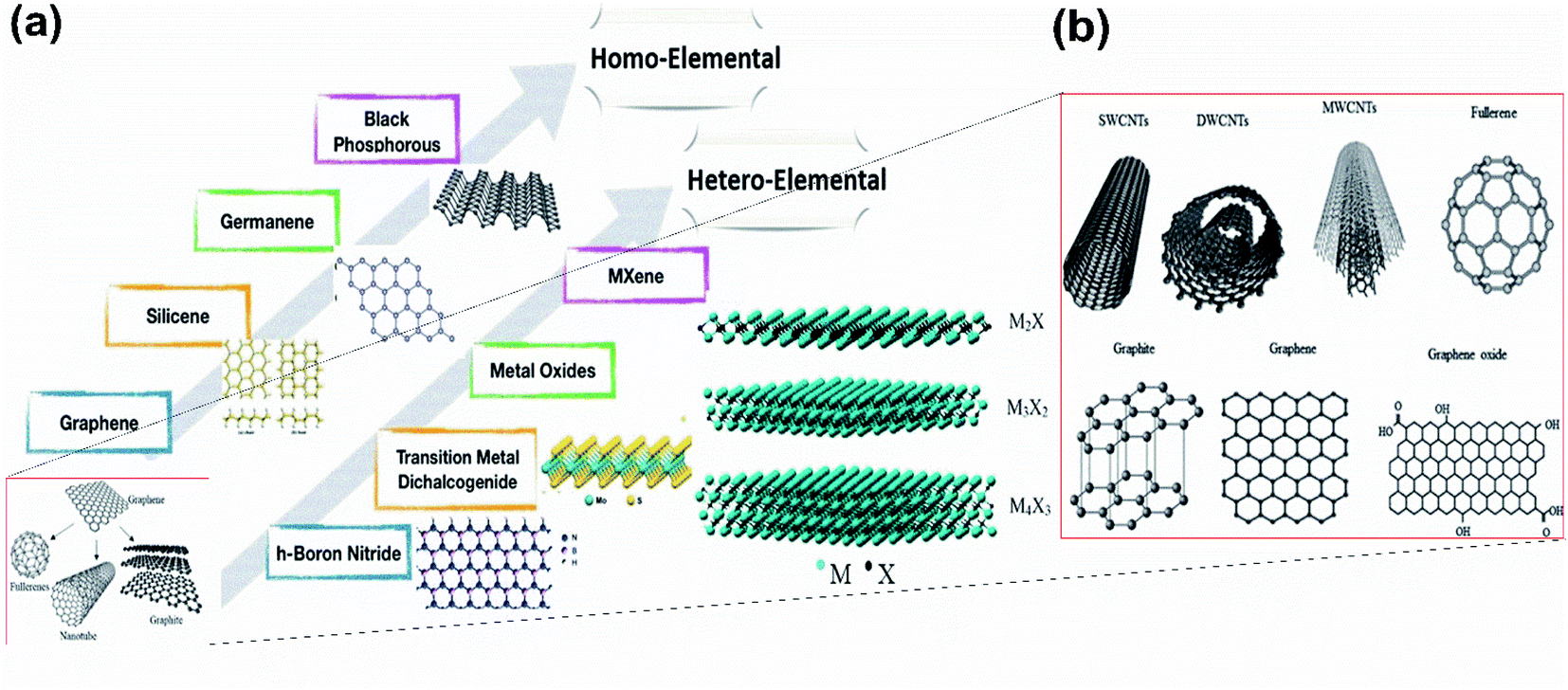 | ||
| Fig. 1 (a) Existing homo-elemental and hetero-elemental 2D materials. (Reproduced from ref. 33 with permission from John Wiley and Sons). (b) Different shapes formed by graphene. (Reproduced from ref. 34 with permission from Elsevier). | ||
Boron is the fifth chemical element of the periodic table, which has valence orbitals like that of carbon (Fig. 2(a, e)) and is the only group 13 (i.e., 3A) element with semiconducting properties.35 For this reason, its 2D form, “Borophene”, also possesses similar characteristics to that of graphene (i.e., a 2D allotrope of carbon)36,37 but has unique polymorphism in contrast to other 2D single-element materials.38–40 Although boron is one of the nearest neighbours of carbon in the periodic table and has similar physical properties, its structure differs from that of graphene due to the difference in their degrees of buckling in the out-of-plane direction (as observed in Fig. 2(b, c and f, g)).41 However, for a buckled borophene with triangular lattice, an important role is played by hydrogen as an acceptor42 as it includes a system that has a surplus of electrons, and after hydrogenation a linearly dispersed Dirac cone as observed in Fig. 2(h), similar to that of graphene in Fig. 2(d), arises in the resulting borophene.43 For this reason, there is still the need for more research on the allotropes of borophene. However, theoretical simulations from the 1990s have revealed interesting properties related to different low-dimensional borophene allotropes.44 Its synthesis in 2015 via the condensation of atoms of hot boron gas on a cool silver surface forced the creation of its hexagonal structure because of the regular silver arrangement. However, the notable proportions of silver and boron (B) atoms have led to the creation of vacancies or holes in the lattice and these vacancy patterns provide unique properties for the borophene crystal.45
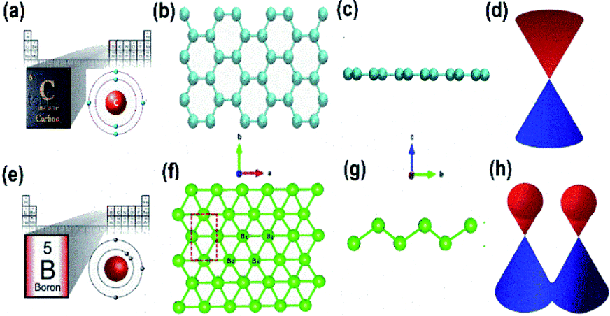 | ||
| Fig. 2 Schematic representation of the valence electrons of (a) carbon and (e) boron respectively in their similar orbital. (Reproduced from ref. 27 with the permission of Elsevier), graphene with (b) top view, (c) side view (reproduced from ref. 46 with the permission of American Physical Society), (d) graphene Dirac cone, borophene (f) top view and (g) side view (reproduced from ref. 31, published by IOP Publishing Ltd, licensed under Creative Commons Attribution 3.0) and (h) Dirac cone of borophene (reprinted with permission of ref. 3. Copyright (2020) Wiley-VCH Verlag GmbH). | ||
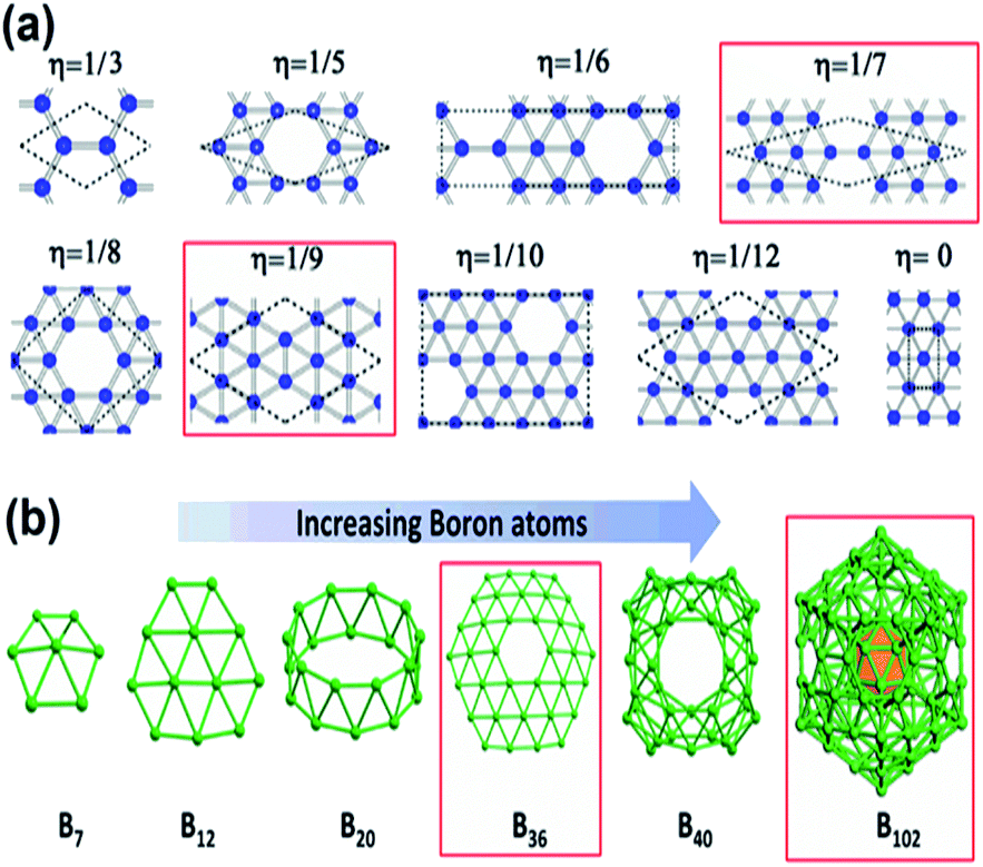
Unlike all other direct experimentally synthesized traditional materials, the borophene design began through theoretical simulations47–49 with the predictions of their probable characteristics,50–52 followed by preparation methods, and then their synthesis in laboratories and their potential applications. This unique strategy is schematically represented in Fig. 3(a),53 and the yearly progress in the publication of borophene papers, is plotted in Fig. 3(b). This emerging development of borophene could be a model for various new materials and a best example for the material genome project (MGI),21 which can improve the synthesis efficiency, minimize the research material cost and increase the material design output rate.
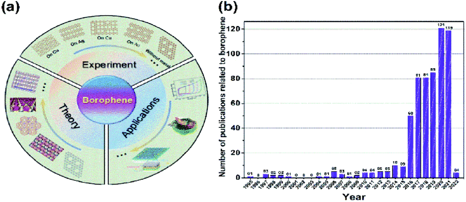 | ||
| Fig. 3 (a) Schematic diagram of the development of borophene. (Reproduced from ref. 54 with the permission of John Wiley and Sons). (b) The number of publications focusing on borophene each year. (From the web of sciences, https://publons.com/publon/). | ||
This paper provides useful information regarding the progress of borophene through previous simulation analyses, experimental confirmation, and different mechanisms for laboratory synthesis. We also report a few of their properties, including the factors that can cause alterations, make comparisons with other 2D materials, and explore their existing applications with updated information to guide researchers in identifying further challenges, and provide opportunities for improvement in various other fields.
2. History of theoretical prediction before experimental confirmation
Until 2015, experimental research on allotropes of nanostructured boron was very sparse due to their toxic and costly precursor (diborane), which was typically suggested.45 However, in the 1990s, using computer simulations, a physicist, I. Boustani, first examined the structure of tiny boron clusters on studying their stability and reported that the final structures mostly preferred the quasi-planar or planar form rather than the icosahedral geometry like that of borane.48 Computational studies have suggested various structures for the 2-dimensional boron sheet50 but in accordance with the general class of quasiplanar clusters of B7 [Fig. 4(a)], Boustani proposed the aufbau principle (inset of Fig. 8(a))47 for constructing nanostructures, which predicted the possibilities of fullerenes of boron (borospherene),55 boron nanotubes30,56,57 and monoatomic sheets of boron (borophene) (Fig. 4(d–f)).49 Since the monoatomic sheet of boron was 2-dimensional and as the traditional rule suggests the fundamental name for the 2-dimensional materials to be ‘Xene’, where X is the element, the monoatomic sheet of boron was named as “Boronene”.58 Further, after analysing the graphene and its aromatic rings of carbon atoms, a monolayer sheet was introduced for the B atoms as well and was called “Borophene”. However, those sheets gave high stability when enhanced by the out-of-plane distortion39,59 or by superstructures of vacancies.30,50 This was because, as a contradiction to graphene, the valency of boron was only three, and it was deficient of a single electron to make sp2 bonding and form a hexagonal lattice as graphene, hence a planar triangular lattice was proposed in the beginning.60 Later, Boustani noticed that the planar triangular lattice was not stable and put forth a buckled structure, i.e., a distortion along its out-of-plane direction from the model of clustered boron in two layers, which consisted of zigzag chains of boron in the up-down direction as seen in Fig. 4(b and c), where its energy for each atom was 0.03 eV lower than the unbuckled one and 0.7 eV lower than the graphene-like honeycomb lattice.61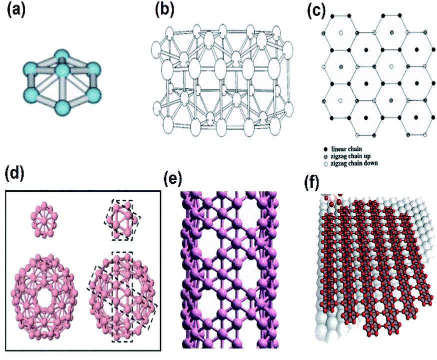 | ||
| Fig. 4 Boron allotropes: (a) quasi-planar cluster of B7 (reproduced from ref. 62 with the permission of Elsevier). (b and c) A double-layered boron cluster, side view and top view, respectively (reproduced from ref. 61 with the permission of AIP Publishing). (d) Fullerene of boron (reprinted with permission from ref. 60. Copyright (2019) Wiley-VCH). (e) A boron nanotube (reprinted with permission from ref. 63. Copyright (2008) American Physical Society). (f) Monoatomic sheet of boron (reproduced from ref. 53, Science and Technology review publishing house licensed under Creative Common Attribution 4.0 international). | ||
In 2005, advanced buckled structures were proposed for borophene as seen in Fig. 5(a–d) and it was determined that the p-orbital symmetries of the B atom were not agreeable with the six-fold coordination in the flat borophene triangular lattice. Hence, via σ–π bond mixing, a buckled structure termed buckled {1212} boron sheet (δ6 borophene) was formed, enhancing the cohesive energy, and when compared with the single-atomic strength of the flat one, it was 0.26 eV stronger.64 In δ6 borophene two different B–B bonds of bond length 1.81 and 1.63 Å were formed, where the height of buckling was ∼0.85 Å.65 Further, ab initio structural optimization disclosed that any random lattice of buckled triangles would relax into δ6 borophene, indicating it as the best structure. Different configurations of borophene including planar reconstructed {1212}, idealized buckled {1212}, icosahedral (bulk boron with α-phase) and few low-symmetry hybrid structures were investigated and among them the most stable structure was the one highlighted in Fig. 5(b), i.e., the buckled {1212}.59
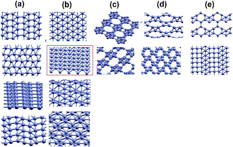 | ||
| Fig. 5 Advanced buckled structures: (a) reconstructed {1212}, (b) idealized and buckled {1212} with the stable one marked in red, (c) icosahedral boron, (d) lower symmetry and (e) few hybrids. Reprinted with permission from ref. 59 Copyright {2007} American Chemical Society. | ||
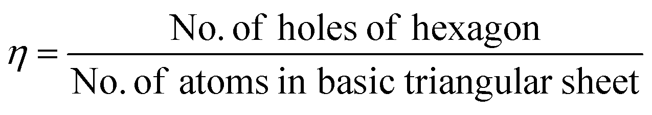
As mentioned previously, the proposed triangular lattice structure, due to the electron deficiency in boron,63,66 can form multicenter-two-electron bonds for stabilizing the structure by buckling.30,67 Later, it was found the flat triangular structure had an excess of electrons, while the hexagonal structure was highly unstable due to the shortage of electrons and for decreasing the energy it requires more electrons. Hence, a mixture of hexagonal lattice, i.e., acceptors and trigonal lattice, i.e., donors, was proposed, which gave rise to triangular motifs of borophene having hexagonal holes30 and predicted that the superstructure vacancies could also improve the stability of the previously proposed flat triangular lattice of borophene. Moreover, a greater cohesive energy was noticed for the hexagonal vacant triangular sheet than the previous one without hexagonal holes.54 This then gave rise to the density parameter,21 based on this, the concentration of hexagonal vacancies could be varied in the motif, where the density parameters were found to be η = 0 and η = 1/3 for triangular and hexagonal sheets, respectively. Depending on the same, various configurations were formed as in Fig. 6(a) but more stability was noted in V1/9 (η = 1/9) and V1/7 (η = 1/7) structures, also termed α-borophene and β-borophene, respectively.21,30,68 Analysis of the calculated band structure of V1/9, designated α-borophene to be metallic63 with the highest cohesive energy/atom.30 A new borophene structure similar to that of α-borophene was proposed with hexagonal holes in parallel and was denoted as the γ-sheet (B36). This γ-sheet was ultra-stable, especially for the B100 cage (highlighted in Fig. 6(b)).69 However, in 2014, based on the outcomes of photoelectron spectroscopy and the simulations of theoretical data, there was a first report on the experimental discovery that the B36 boron cluster was quasiplanar with high reliability and consisted of a predominant hexagonal hole and hence it was potentially viable for reproducing sheets of single-atomic layered boron on a larger scale with hexagonal vacancies.50
 | ||
| Fig. 6 (a) Various density parameter-dependent configurations with two stable structures marked in red. (Reproduced from ref. 70 with the permission of AIP Publishing). (b) Structural variation with an increase in the number of boron atoms. (Reproduced from ref. 58). | ||
A better understanding of α-borophene was given by Galeev et al.71 by reporting about its fragments along with chemical bonding, wherein an adaptive natural density partitioning (AdNDP) method was used. As seen in Fig. 7(a) α-borophene was classified with regard to ‘n’center-2 electrons, where n = 2,3 and 4 in σ-bonds and n = 6 and 7 in π-bonds, but there was instability in the borophene structure when the σ![[thin space (1/6-em)]](https://www.rsc.org/images/entities/char_2009.gif) :π electron ratio was 0.5.71 Subsequently, various possible borophene structures, as seen in Fig. 7(b), were constructed by the cluster expansion (CE) method and named B1−x ⎔x, with ⎔ as the hexagonal vacancy. Those configurations were different in structure, dependent on x = 0.1–0.15 but they had nearly similar energy formations, especially for borophenes with x = 1/9, 1/8 and 2/15, which were also analyzed as shown in Fig. 7(b). At room temperature, on taking KBT = 0.026 eV, the substrate-independent borophene mostly preferred to have a polymorphic structure.72 As seen in Fig. 7(c–f) several complexes of borophene were predicted via the swarm optimization (CALYPSO) code, and the α-sheet was the ground state among the independent borophenes.73 Since the energy difference was very narrow between V1/8, V2/15 and α(V1/9)-borophene, GGA-PBE was less effective for ensuring their relative stability, hence their cohesive energy was calculated using a hybrid functional PBE0,74 where α1-borophene showed 136 meV per atom higher energy than the α-sheet, and β1-borophene showed 118 meV per atom and 96 meV per atom high stability than the β-sheet and α-sheet, respectively. However, V1/8 and V2/15 had approximately the same cohesive energy and were much more stable (i.e., 30 meV per atom) than α-borophene.30,74,75 Hence, the α-sheet, previously trusted as the ground state, was proven wrong.
:π electron ratio was 0.5.71 Subsequently, various possible borophene structures, as seen in Fig. 7(b), were constructed by the cluster expansion (CE) method and named B1−x ⎔x, with ⎔ as the hexagonal vacancy. Those configurations were different in structure, dependent on x = 0.1–0.15 but they had nearly similar energy formations, especially for borophenes with x = 1/9, 1/8 and 2/15, which were also analyzed as shown in Fig. 7(b). At room temperature, on taking KBT = 0.026 eV, the substrate-independent borophene mostly preferred to have a polymorphic structure.72 As seen in Fig. 7(c–f) several complexes of borophene were predicted via the swarm optimization (CALYPSO) code, and the α-sheet was the ground state among the independent borophenes.73 Since the energy difference was very narrow between V1/8, V2/15 and α(V1/9)-borophene, GGA-PBE was less effective for ensuring their relative stability, hence their cohesive energy was calculated using a hybrid functional PBE0,74 where α1-borophene showed 136 meV per atom higher energy than the α-sheet, and β1-borophene showed 118 meV per atom and 96 meV per atom high stability than the β-sheet and α-sheet, respectively. However, V1/8 and V2/15 had approximately the same cohesive energy and were much more stable (i.e., 30 meV per atom) than α-borophene.30,74,75 Hence, the α-sheet, previously trusted as the ground state, was proven wrong.
 | ||
| Fig. 7 Complexes of borophene: (a) n-center, 2-electron (reproduced from ref. 71 with the permission of the Royal Society of Chemistry), (b) cluster expansion (CE) method (reprinted with permission of ref. 72. Copyright (2012) American Chemical Society), (c–f) CALYPSO code (reprinted with permission from ref. 74 Copyright (2012) American Chemical Society), (g, h) buckled structures with small thicknesses and 2 × 2 × 1 supercell projections along [001] and [100] for (g) Pmmn-boron and (h) Pmmm-boron. (Reprinted with permission from ref. 60. Copyright (2019) Wiley-VCH). | ||
Besides these, two more buckled structures, having non-zero thicknesses, namely Pmmn (Fig. 7(g)) and Pmmm (Fig. 7(h)), were also predicted. The results of the HSE06 (GGA-PBE) calculation showed the ultra-stability of the Pmmn/Pmmm sheet as compared to the α-sheet but their stability relations are yet to be studied. The Pmmn phase having low symmetry with the linearity of the Dirac dispersion similar to graphene was identified to be semi-metallic.39 All these predictions were only for the substrate-independent borophene and all of them showed perfect single-crystallinity. Nevertheless, substrate-supported borophene varied in stability and offered many more new, mixed structures.
The dynamical instability in the proposed freestanding borophene32 motivated many researchers to find various methods for improving their stability, which included surface functionalization and adsorption on substrates.28,32,76,77 After analyzing the growing mechanism of graphene and silicene on the metal surface, the metal-based substrates were regarded to be a productive way for finding the solution for borophene sheets.54 Through theoretical calculations, numerous 2-dimensional boron allotropes in Fig. 8(a) were reported,36,67,78,79 wherein the computational studies by Liu et al.80 proved that they could be extracted by the deposition of boron sources on the substrates of Au, Ag, Cu or metal bromides (MgB2).80 Again, using swarm optimization (CALYPSO), numerous complexes were predicted on the surface of Ag/Au/Cu/Ni and their results in Fig. 8(b) indicated their structural variations at the respective ground states for different metal substrates. Later, on identifying a large difference in the lowest energies of the two structures formed on Cu, V1/6 sheets, Pmmm were found to be much more stable on Cu.81 It was also found that resultant 2D boron clusters on Cu(111) contained holes and it was observed that nucleation of the 2D cluster by Cu substrate could easily form hexagonal holes.82 This was an essential framework that led to other successive theoretical predictions. Further, based on the first principles calculation via surface structure search and the CE method, the borophene sheets were systematically investigated and resulted in a hexagonal-holed triangular pattern when grown on Cu, Au, Ni and Ag, where icosahedral β12 was not favorable on Ni and Cu but was minimum on Au and Ag, which indicated that those metals could promote the nucleation as represented in Fig. 8(c) within boron sheets and donate extra electrons for stabilizing it.81 Successively, the predictions were experimentally confirmed initially in the same year (2015) by Mannix et al.,45 using Ag(111) as the metal substrate.45 Furthermore, corresponding experiments on same substrate showed that it could cause nucleation and donate electrons for stabilization and reported β12 (η = 1/6) to be the ground state.15 Presumably, under ultra-high vacuum conditions, four phases of borophene, namely the 2-Pmmn phase, β12 phase, χ3 phase and graphene-like honeycomb phase were developed successfully on Al/Ag/Au/Cu(111) substrates,15,51,53 which are discussed in detail in Section 3.
 | ||
| Fig. 8 (a) Theoretically simulated borophene structures with yearly categorization. (Reproduced from ref. 54 with the permission of John Wiley and Sons). (b) Stability versus hole density under vacuum and on Au, Ag, Cu and Ni substrates with structures formed at their different energy states. (Reprinted with permission ref. 81 Copyright 2015, Wiley-VCH). (c) Schematic representation of boron sheet nucleation over the metal substrate for its stabilization, (reproduced from ref. 83). | ||
3. Synthesis of 2D borophene
The 3D boron bonding configurations,32 accompanied by a large difference in energy as compared with the 2D form,84 make the fabrication of borophene a challenging task. Usually, this requires ultralow pressures and sophisticated facilities for its fabrication.3 Even then, on considering the theories, borophene synthesis was possible via the bottom-up approach,15,18,45,85 top-down approach,86–88 exfoliation techniques (i.e., sonochemical, liquid phase),87–89 deposition techniques (i.e., CVD, PVD)32,90–92 etc. It gave raise to different complexes of borophene, which were either supported by a substrate, or independent (i.e., freestanding) one.933.1. Growth of borophene supported on a substrate
Due to the presence of periodic hexagonal holes in borophene or hexagonal boron (highlighted in Fig. 6(b)) within its triangular lattice, theoretically, it was very stable63 when supported on metal substrates such as aluminium Al(111),94 silver Ag(111),15,45 gold Au(111)95 or copper Cu(111).82,96 This was achieved through various fabrication methods such as atomic layer deposition, molecular beam epitaxy, chemical vapor deposition, and so on. The merit of these method includes the chemical purity of the obtained borophene for the further study of the chemical and physical behaviours.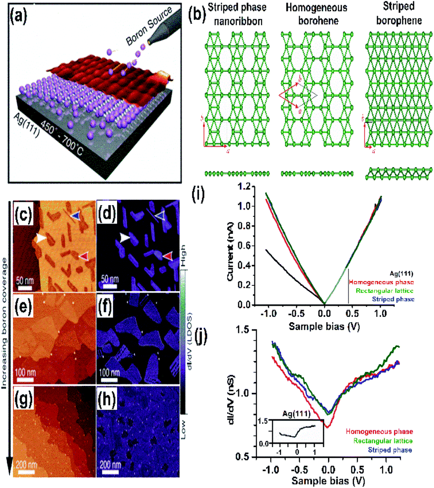 | ||
| Fig. 9 (a) Schematic representation of the atomic layer deposition of boron on Ag(111), (b) three phases formed at 550 °C (reproduced from ref. 97, published by Taylor & Francis Group, licensed under Creative Common Attribution). (c–h) Series STM topography in large-scale (on left) and dI/dV closed-loop (on right) images for the borophene sheets, where (c and d) shows low coverage of boron, (e and f) medium coverage of boron, (g and h) high coverage of boron, with blue, red and white arrows indicating the striped phase nanoribbon, homogeneous-phase and striped phase of borophene (reproduced from ref. 21, published by Wiley-VCH GmbH, licensed under Creative Common Attribution 4.0 International). (i and j) I–V curve and dI/dV spectra indicating the metallic characteristics of the resulting boron sheets. (Reproduced from ref. 53. Published by Science and Technology Review publishing house, licensed under Creative Commons attribution 4.0 international). | ||
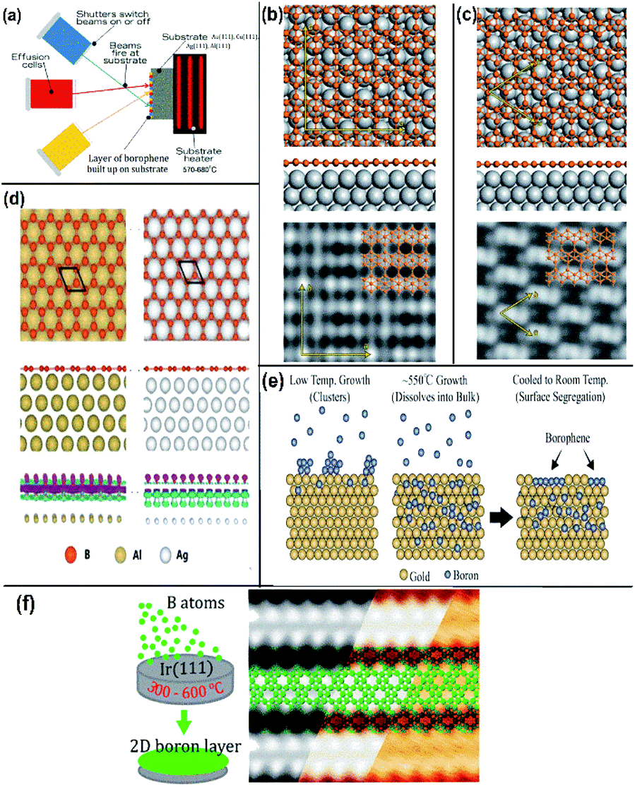 | ||
| Fig. 10 (a) Schematic MBE method representation, (Published by GO LOOK IMPORTANTBOOK), (b and c) (from top to bottom) top view, side view and STM image of (b) β12 and (c) χ3 on Ag(111), (reproduced with the permission of ref. 25. Copyright (2019) Wiley-VCH Verlag GmbH) (d) borophene (honeycomb structure) on Ag(111) and Al(111) represented with different colours as mentioned (from top to bottom) top view, side view and the electron density map, (reproduced from ref. 51 with permission of Elsevier). (e and f) Schematic borophene growth on (e) gold substrate, (reprinted with permission from ref. 95. Copyright (2019) American Chemical Society) and (f) iridium substrate with its STM image (reprinted with permission from ref. 100, Copyright (2019), American Chemical Society). | ||
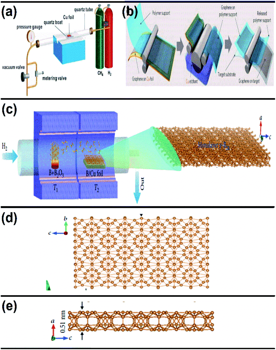 | ||
| Fig. 11 Schematic representation of (a) the CVD graphene system at a controlled pressure, (b) the transfer of the synthesized graphene to the target substrate (reproduced from ref. 91 with permission from the American Chemical Society). (c) Diagram of the furnace with two zones for the growth of borophene on Cu via CVD. (d) Top view and (e) side view of the resultant borophene obtained in (c). (Reproduced from ref. 92 with permission of John Wiley and Sons). | ||
An improvement in the CVD technique was noticed when micrometer-sized borophene was grown over a thick Cu(111) film on sapphire, in which the boron was repeatedly submersed into the Cu at a high temperature, and at low temperature it was recrystallized and resurfaced. Through this technique, the size of the wafer was scalable, copper film could be relinquished and sapphire could also be reused.96 Furthermore, an efficient technique namely, van der Waals epitaxy was used for growing borophene on a larger scale via CVD in a furnace with two zones. An additional intermediate of metastable boron cluster was formed by annealing sodium borohydride powder [NaBH4] (i.e., boron source), the polymer and substrate chosen were fluorophlogopite mica (KMg3AlSi3O10F2)98 and polymethyl methacrylate (PMMA), respectively. Recently, CVD was employed for synthesizing borophene on Ni foil to get a semiconductor having a direct band gap with tunable properties.98
3.2. Free-standing borophene sheets
Due to the myth that bulk boron forms non-van der Waals crystals,103 the fabrication of free boron nanosheets is considered challenging; however, there have been a few recent findings on free-standing (i.e., independent) borophene by methods like exfoliation and the modified Hummers' method, which have completely broken the myths.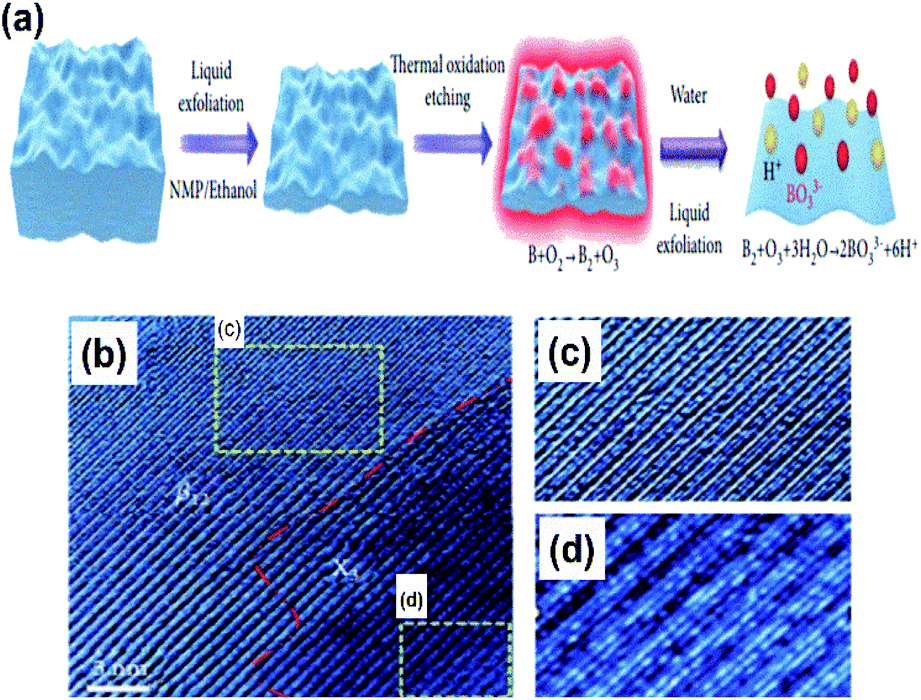 | ||
| Fig. 12 (a) Schematic micromechanical exfoliation representation by the top-down approach. (b) Electron microscope image of the resulting borophene sheet. (c and d) Zoomed images of the (c) β12 and (d) χ3 phases observed in (b) (reproduced from ref. 53 Published by the Science and Technology Review Publishing House licensed under the Creative Common Attribution 4.0 International). | ||
Mixing the required nanosheet in a suitable solvent is given in terms of a thermodynamic equation:
 | ||
| Fig. 13 Schematic representation of the modified Hummers' method. (Reproduced from ref. 104 published by MDPI, licensed under the Creative Commons Attribution). | ||
| Method | Merits | Demerits | References | |
|---|---|---|---|---|
| Substrate supported | Atomic layer deposition | • High-quality ultra-thin film | • Time consuming chemical reaction | 45 |
| • Excellent repeatability | • Very high material and energy waste rate | |||
| • High film density | ||||
| • Large area thickness uniformity | ||||
| • Atomically flat and smooth surface coating | • Obtaining ultra-high vacuum condition is challenging and costly | |||
| • Low-temperature processing | ||||
| Molecular beam epitaxy | • Extremely pure/clean borophene | • Very slow and laborious method. i.e. growth rate few micrins per hour | 15, 51 and 95 | |
| • Ultra-thin film | ||||
| • High uniformity with less defect | ||||
| Plasma enhanced CVD | • Industrial scale synthesis possible | • Time-consuming | 32, 91, 92, 96, 98, 101 and 102 | |
| • No requirement of high vacuum level | • Costly equipment | |||
| • High thermal and chemical stability | • Instability to humidity | |||
| • Corrosion-resistant | ||||
| Freestanding | Micromechanical exfoliation | • Uniform layered high quality | • Slight changes in conditions/parameters cause irreversible changes in the structure | 88, 89, 103 and 104 |
| • Larger lateral dimensions with different layers | • Choice of suitable and adequate solvent is tedious | |||
| Modified Hummers' method | • Oxidation level improved | • Time-consuming process | 93 | |
| • Enhanced product performance | • Tedious purification process |
On comparing the overall scalability of the process with that of graphene, it was revealed that an allotrope of carbon, i.e., graphite, being the starting material of graphene, is a non-metallic and tetravalent element, which is the 15th most abundant element in the Earth's crust and the 4th most abundant element in the universe, hence is easily available in a larger quantity and has a wide application. However, boron, the starting material for borophene, occurs on the Earth in a significant concentration known as borate mineral, which is of 100 different types but the most common ones are borax, kernite and ulexite; their cost is ten times higher when compared to that of graphite.
4. Properties
Given the interesting facts about borophene, its promising contribution is suggested for sensing and electronic applications, hence numerous studies have been devoted to understanding borophene's properties and structure. A detailed discussion regarding a few major properties such as high mechanical properties, electronic or ionic conductivity, lattice thermal conductivity, super conductivity, optical properties, atomic adsorption, surface reactivity and high capacity are mentioned in some of the review articles.3,53,54,105After understanding the borophene structure as discussed in Section 2 it is important to introduce its properties. The natural 3D boron structure indicates that it is an intermediate of both metals and non-metals, i.e., it is a metalloid and is used commonly in semiconductors.106 Even then, due to its electron deficiency along with multicenter bonds,32,76,77 boron is gifted with some interestingly unique desirable properties when it is in its 2-dimensional form, i.e., as borophene. Among the borophene allotropes, 2-Pmmn, χ3 and β12 phases include properties like mechanical flexibility, metallicity, transparency, superconductivity, selectivity, sensitivity, etc.
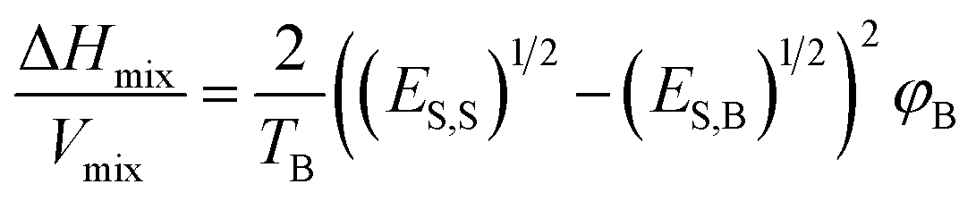
4.1. Mechanical properties
The scientific research communities have shown great interest in the mechanical properties of borophene due to its mechanical modulus with ultrahigh value, strong B–B bonds and uniqueness in atomic structures107–109 and have described that chemical modification, number of layers, temperature and the vacancy defects of borophene also contribute to their unique mechanical properties,110 and its mechanical strength can be determined by a few of the interpretative parameters including lateral size, anisotropy, reduced dimensionality, and disparate polymorphs.For studying the chemical modulation effect, researchers have been performing physical and theoretical experiments on different borophene forms to find their mechanical coefficients.111 Nonetheless, few results have disclosed that there is a decrease in the coefficients of different forms of borophene due to electrochemical fluorination. It has been reported that after the fluorination of 2-Pmmn borophene, two anisotropic structures B2F and B4F,112 with high stability were obtained, which showed good thermal, electrical and mechanical conductivity properties and were thus identified as encouraging candidates for electronic devices as semiconductors.106 Similarly, on hydrogenation of borophene (borophane), the Young's modulus of 2-Pmmn phase along its zigzag and armchair directions decreased to 110.59 and 172.24 N m−1, respectively, indicating an increment in mechanical flexibility.111 The reason for the decrease in Young's modulus was investigated and it was proved that on hydrogenation the B–B bonds become elongated from 1.616 Å to 1.941 Å, leading to the bond strength decrement, which reduces Young's modulus. Moreover, critical strain increased along all three directions (zigzag, armchair and biaxial) after the hydrogenation (a comparison of borophane with other 2D material is shown in Fig. 14(c)),50,111 which maintained its stability until the tensile uni-axial strain along the zigzag and armchair directions was up to 22% and 17%, respectively.113 Later, the analysis of α1-borophene and γ-B28 (ref. 92 and 114) showed that boron sheets are able to open a new bandgap after hydrogenation, which can act as a semiconducting material.
 | ||
| Fig. 14 (a) Diagram showing the mechanical flexibility of borophene. (Reproduced from ref. 105 with permission from Elsevier). (b) Comparison of the electronic DOS for the densest borophene (S1) and borophene with an increase in vacancy defect concentration (S2–S5) across the armchair direction with respect to different strains (ε) and at maximum tensile strength (εuts). (c) The ratio of overall strain in the zigzag (ηZZ) and armchair (ηAC) directions for different 2D materials. (Reproduced from ref. 111 with the permission of the Royal Society of Chemistry). (d and e) Variation in Young's modulus across the (d) armchair direction and (e) zigzag direction with an increase in the conc. of vacancies from (S1–S5). (Reproduced from ref. 108 with the permission of the Royal Society of Chemistry). | ||
The study of multi-layer borophene of the 2-Pmmn phase was able to relate the variation in the mechanical properties due to the effect of change in the number of layers, wherein Young's modulus was measured as 136 N m−1, 141 N m−1, 144 N m−1, 158 N m−1 along the zigzag direction, and along the armchair direction it was 338 N m−1, 360 N m−1, 380 N m−1, 397 N m−1 on varying from a four-layered borophene to a monolayered one, respectively, revealing that Young's modulus is maximum for the one with four layers. Hence, borophene exhibits superior mechanical properties similar to black phosphorene on increasing their layers.115 A monolayered borophene is extremely flexible and is indicated as a promising nanomaterial for wearable devices.53
It was found that when boron concentration was 4/27th of the total borophene concentration, along the zigzag direction, Young's modulus reduced from 180 N m−1 to 87 N m−1 when the temperature was increased from 1 K to 600 K, indicating the inverse proportionality of Young's modulus with temperature.115
The results of mechanical properties seen in Fig. 14(d and e) revealed the inverse proportionality of Young's modulus to vacancy defect along the armchair direction, and Fig. 14(b) revealed the inverse proportionality of borophene density of states to vacancy defect concentration, which also decreased its tensile strength.108 Borophene with phase β12 and χ3 had a much smaller Young's modulus when compared to the 2-Pmmn phase across the armchair direction, whereas along the zigzag direction, Young's modulus was not much affected by the vacancy defects. Along with this, it was observed that for α sheet, β12 and χ3, the critical strains across both in-plane directions were much larger when compared to the defect-less 2-Pmmn phase borophene. Nevertheless, the atomic displacement method indicates that an increase in hollow hexagons reduces B–B bonds, causes a stiffness change in borophene, and increases the hardness of the material, indicating the effect of hollow hexagons on its mechanical strength.31,67
4.2. Chemical properties
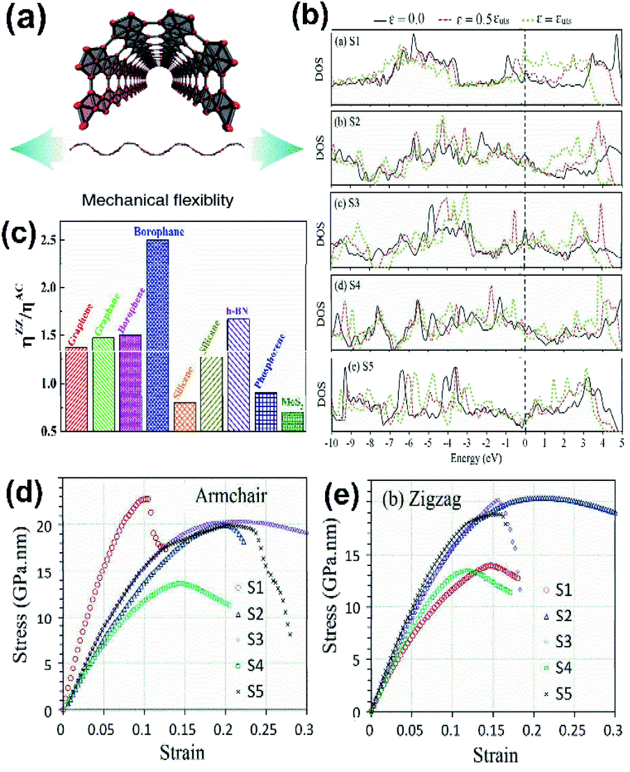
Focussing mainly on the reactivity of borophene during the chemical reaction, i.e., metallicity, boron ([He]2s22p1) located between carbon (nonmetallic) and beryllium (metallic), exhibits both metallicity and non-metallicity due to the presence of 2p electrons along with orbit radius near the 2s state.41,116 One of its interesting facts is that its 2-dimensional structure shows intrinsically high anisotropic metallic properties7 and few of its allotropes with Dirac fermions are also semi-metallic.39 Along with allotropes 2-Pmmn, χ3 and β12, the honeycomb borophene phase also exhibits metallic behavior,117 diverging from its triangular and hexagonal lattice structures.30 These metallic characteristics were predicted theoretically by Zhang et al.81 and experimentally confirmed through the STM data.15 The theoretical results118 in which the two bands crossing the Fermi energy as in Fig. 15(c) and the dispersion of the Fermi surfaces EF = EBS(kx,ky) throughout the Brillouin zone as in Fig. 15(d) are in agreement with the previous studies,61,119 and revealed that borophenes are metallic. When compared with the spin–orbit couplings of other 2-D materials and graphene, borophene has a negligible spin–orbit coupling and is considered the lightest 2D material showing metallic properties in which there was linear dependence of energy on momentum, i.e., a Dirac metallic material.120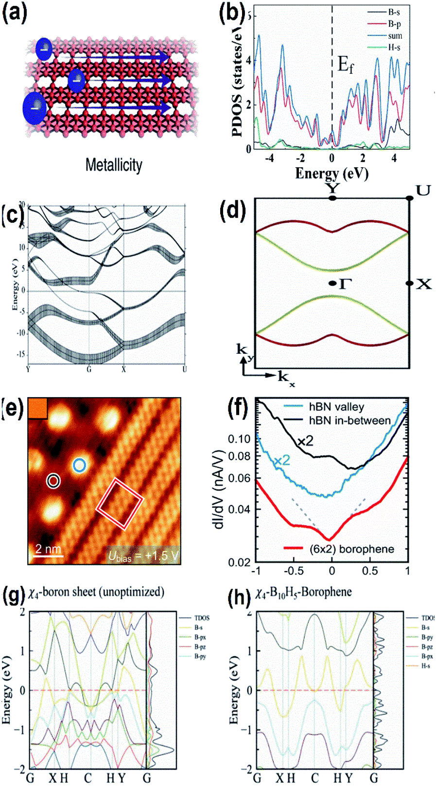 | ||
| Fig. 15 (a) Diagram showing the metallicity of borophene, (reproduced from ref. 105 with permission from Elsevier). (b) DOS with electronic band structure for α1-2H borophene with different colours for different orbitals of borophene (where blue: total DOS, black: B-s, red: B-p, green: H-s) with respect to the valence band maximum. (Reprinted with permission from ref. 98. Copyright (2021) American Chemical Society). (c) Band structures for the sheets of borophene plotted along high symmetry points; fat bands indicate the sp character of the σ-bond, where the Fermi energy lies at E = 0 and the Γ point is represented by G. (d) The 2-dimensional Fermi surface of the electronic energy (EE) bands crossing the Fermi energy in (c) is represented in red and yellow. (Reprinted with permission from ref. 118, Copyright (2019–2020) American Physical Society). (e) STM image of (blue circle) valley hexagonal boron nitride, (black circle) mesa hexagonal boron nitride, (red square) borophene. (f) dI/dV spectra representing the images marked in (e) in their respective colours. (Reprinted with permission from ref. 99 Copyright (2021) American Chemical society). (g, h) Band spectrum including TDOS and PDOS of χ4-borophene with (g) no hydrogen atom and (h) 5 hydrogen atoms. (Reprinted with permission from ref. 121, Copyright (2021) American Chemical Society). | ||
Based on the PBE functional, DOS corresponding to the band structure of α1-2H borophene indicated in Fig. 15(b) proved its metallicity recently, which was in agreement with the UV-visible and PL results.98 Further, a distinct metallic property was observed when borophene formed a heterostructure with any other 2D materials.32
By the technique of thermal decomposition, a newly introduced borophene on Ir(111) also showed metallic character as specified by the results of the dI/dV curve in Fig. 15(eand f), where the decrement in the Fermi level to form a V-shape is partial evidence for borophene on Ir(111) showing the Dirac-like behavior.99 The presumed electronic band structures of χ4-5H-borophene indicated in Fig. 15(g and h), disclosed its metallic behavior based on the Density Functional Theory (DFT) through the Vienna ab initio Simulation Pack (VASP),121 where the metallic behavior is significantly contributed by the p-orbitals, which is comparable to previous reports122 indicating χ4-5H-borophene to be suitable for employment in the applications of memory devices as well. Moreover, the same can also be identified by the 3 bands (2 in the G–X direction and 1 in the S–Y direction) in the Fermi level.7 The metallic structure of a single-layered borophene was due to the overlapping of their electronic bands at the Fermi level45 in which the metallic states were predicted to originate due to the appearance of the band gap near the Fermi level as a result of their corresponding 2px and 2py states.54
Chemical modifications like hydrogenation, fluorination, and lithiation can also affect the metallic properties.110 On hydrogenation, the band structure of the 2-Pmmn phase changes to that of a semiconductor with zero bandgap and even in a state free of stress, a metallic band structure is observed in graphene-like borophene, and a biaxial or uniaxial shear strain can cause the transition of the metallic band structure to a semiconducting one (Fig. 16(a–c)).123 The theoretical results of fluorinated borophene were investigated and the energy band structure as shown in Fig. 16(d–f) revealed that B4F is metallic and B2F is an indirect semiconductor.112 Metallic characteristics were exhibited by the electronic structures during the lithiation process,124 indicating that borophene is an excellent electronic conductor with high ionic conductivity. Moreover, the β12 and χ3 phases when used as an anchoring material in Li–S batteries showed electronic structures with metallic properties during their entire discharging and charging cycles.110 As predicted previously, even the PDOS of the borophene heterostructure with Li proved that the lithiation process does not diminish the metallicity of the entire system completely (Fig. 16(g and h)),125 whereas the interactions of halogen atoms or molecules with borophene, do not alter its metallicity.126
 | ||
| Fig. 16 (a) Dispersion of phonon for W-borophane (completely hydrogenated borophene) under different shear strains. (b–f) Electronic band structures of W-borophane: (b) with H vacancy, (c) with a dimer (B–H) vacancy. (Reproduced from ref. 123, published by Royal Society of Chemistry licensed under Creative Common Attribution Non-Commercial 3.0 Unsupported license). (d) Pure borophene, (e) B4F, (f) B2F, (reproduced from ref. 112, published by ACS Author Choice). (g) Total and partial DOS of borophene, graphene, borophene/graphene. (h) Total DOS of B/G with single Li (reprinted (adapted) with permission from ref. 125. Copyright (2020) American Chemical Society). | ||
These metallic features of borophene are useful for the sensing of various small molecules and gases although it depends primarily on the electronic structure.127 Since metallic borophene consists of abundant electrons, it can be used for catalysis as well.128 It has been predicted that even the conventional superconductivity mediated by phonon is due to the intrinsic metallicity.32
4.3. Electrochemical properties
Electrochemical properties are among the most essential for various applications such as energy storage and sensing, and researchers are still finding ways to improve the electrochemical properties of existing nanomaterials that are already used as sensors, as well as finding new efficient materials for the same. The atomic configuration is one of the important parameters that has opened up platforms for the development of sensors and interestingly, in the case of borophene, rather than the usual binding, the existence of additional electron-deficient bonds inspires it towards the sensing properties.3 However, the comparatively low conductance of borophene identified during the previous reports on their electronic properties5 is one of the main motives for sensing hydrogen coverage. Moreover, electron mobility along with metallic structure is necessary for exhibiting various sensing properties including photonic, electronic, thermoelectric and thermal sensing for numerous small molecules and gases.129 The adsorption of ammonia130 and HCN105,131 is one of the parameters that suggests that B36 can sense ammonia and HCN; there was a variation in the electronic properties at the B36 edges when compared to its other configurations.105 Recently Wu et al.98 reported the photosensitive properties of PMMA-supported borophene through the results of photocurrent versus reverse bias on varying the light power (Fig. 17(b)).98 The Fe3O4 nanoparticles, when functionalized by borophene to result in χ4-borophene, exhibited good sensing properties due to the core–shell structure.121 Ultrasensitive molecular sensing could be delivered by borophene due to its ridgelines (an excellent molecule anchor) along with light and strain sensitivity.103 | ||
| Fig. 17 (a) Diagram indicating the anisotropic and polymorphous structure of borophene favoring its properties like transparency and superconductivity. (Reproduced from ref. 105 with permission from Elsevier). (b) Variation in the photocurrent vs. reverse bias on PMMA-supported borophene (reprinted (adapted) with permission from ref. 98. Copyright (2021) American Chemical Society). (c) Vertical and (d) horizontal variations in I–V curves for bare borophene (black) and on addition of NO (red). (Reprinted (adapted) with permission from ref. 138. Copyright (2018) American Chemical Society). (e) Band structures and DOS with Fermi-energy aligned initial energy. (Reproduced from ref. 137 with the permission of IOP Publishing Ltd.). (f) Graph of wavelength (λ) and transition temperature (Tc) vs. the vacancy concentration of boron (η). (Reproduced from ref. 70 with permission from AIP Publishing). | ||
Although there are rare reports on the sensing property of substrate-supported borophene, the first synthesized independent borophene sheets by Ranjan et al.93 showed its ability to sense the gas, strain and molecules based on the surface-enhanced Raman spectroscopy (SERS). Even though both β12 and χ3 phases of borophene exhibited metallic behavior, only the β12 phase has the ability to sense the molecules with the help of electrical signals due to the increment in the mobility of electrons along the ridgelines.132
Firstly, the sensing property of borophene was identified by the first-principles calculations.105 Theoretical analysis through DFT calculations have indicated the suitability of borophene particularly for the toxic gas sensing wherein the adsorption of NH3, NO2, CO2, NO and CO gas molecules was observed by analyzing the transport and electronic properties of borophene sheets within the Perdew–Burke–Ernzerhof exchange-correlation functional and generalized gradient approximation using VASP27, and it was observed that the binding energy was low for CO2 molecules and high for the remaining gases.133 The theoretical results using the Cambridge Sequential Total Energy Package (CASTEP) also revealed that borophene could be an actively good material for the sensing of CO2 molecules.134 Similarly, the adsorption of NO, H2, N2, O2, H2O, CO and NO on B36 sheet revealed by the DFT results indicated that B36 can detect NO, CO and O2.131 The employment of the Minnesota 06 and B97D functionals using DFT predicted the increase in the electrical conductivity in the presence of formaldehyde, which indicated that B36 exhibited the property of sensing formaldehyde.135 Furthermore, there have been findings of borophene with electronic and energetic sensitivities for nucleobases (adenine, cytosine, guanine and thymine).136
Borophene is highly sensitive for the detection and transmission of electronic signals.135 The sensitivity of borophene can be further enhanced for transforming stimuli such as pH and temperature into mechanical, optical and electrical signals when combined with hydrogel-based substrates.81 Lherbier et al.137 proved the improvement in the photosensitivity of borophene through its surface modifications. Also, their high surface volume ratio is one of the favorable properties for detecting gas molecules with low concentration. As observed from the results of I–V characteristic data as shown in Fig. 17(c and d), borophene showed the variation in its electrical properties with the addition of NO; the decrease in band gap and change in the adsorption energy when treated with ethanol also indicated the sensitivity of borophene for ethanol vapor.138 Further, the property of gas adsorption for spintronic and gas sensor devices could be improved by embedding borophene with the atoms of transition metals.139 Hence, the outstanding sensing properties of borophene has helped it to emerge in various fields.
4.4. Electrical properties
Borophene with a combination of high electrical, ionic, optical and thermal conductivities serves as an outstanding material for various applications.110 Herein, we mainly focus on its electrical and thermal conductivity. For borophene with the 2-Pmmn phase, the electrical conductivity is higher along the armchair direction when compared to that of the zigzag direction.123 Studies on the electron–electron and electron–phonon interactions by state-of-the-art methods showed that electrical conductivity is controlled by electron–phonon interactions38 and as seen in Fig. 17(e), an important role is played by the Fermi velocity for the electrical conductivity when the electron–phonon relaxation time is closer to the Fermi level (EF) and the density of states is at EF.137 Moreover, the conduction of electricity is facilitated by the construction of metallic bands in borophene. Along with this, the tendency of borophene to donate electrons motivated the research on halogen atom (F, Cl, Br, I) interactions with borophene, and on analyzing the single halogen migration on borophene surface it was observed that high diffusion barriers which decrease with atomic size were able to alter the anisotropy of electrical conductivity.126 The electrical conductivity of the electrode can be further improved when Li/Na atoms are absorbed by borophene, showing its metallic property, which has low open-circuit voltage when treated as the anode material105 and especially during the complete lithiation process the electrical conductivity of borophene was excellent due to the metallic characteristics observed in its electronic structure.124 In a study,136 the variation in electrical conductivity was also observed when B36 borophene was in contact with different nitrogenous bases. The boron vacancy and good electronic conductivity of borophene highlight its ultrahigh ionic-conductivity at its 2-Pmmn phase representing its best performance during it discharging and charging cycles.124The thermal conductivity of borophene was reported to be much low due to its anisotropy when compare to other similar isotropic 2-dimensional materials.45 The results of borophene grown on Ag(111) showed low thermal conductivity at its lattice, which was strongly anisotropic as the phonon–phonon scattering was very strong and could be further reduced when the length of the lattice was reduced below 300–400 nm.140 Using DFT, on solving the Boltzmann distribution for phonon frequency, the thermal conductivity of δ4 borophene after intercalating it with Al was studied and it was found that thermal conductivity increased along the armchair as well as in the zigzag direction, even though the atomic density of intercalated borophene was large. This was because of the grouping of the acoustic branches in borophene after the intercalation, which decreased the phase space of the phonon scattering process. Along with this, even the anisotropy also got tuned.141 Mortazavi et al.142 calculated the thermal conductivity through the molecular dynamics at non-equilibrium and observed the effects of strain, where the thermal conductivity of borophene increased largely when strained along the armchair direction, i.e., 250% increment and the increase in thermal conductivity was much less when strained along the zigzag direction, i.e., a 20% increment for a strain of 8%.142
Recent investigations on the diffusion property of lithium in the heterostructure of borophene/graphene revealed that the overall conductivity of borophene could be further enhanced through the borophene/graphene heterostructure.125 The study of the optoelectronic properties of δ6 and β12 via the perturbation theory and DFT revealed that both allotropes of 2D boron are optically transparent, which strongly depends on the energy and thickness; a weak absorbance was also observed in the visible range. This also introduced borophene as a good material for nano-optoelectronics with tunable monolayers.
4.5. Magnetic properties
Various 2-dimensional materials, especially Dirac materials, are being investigated based on their superconductivity behavior143 and it was reported that graphene becomes superconducting when heavier atoms are doped into it.144 Similarly, borophene being another 2D Dirac material is also reported to show superconductivity properties79,116,145,146 due to its low mass along with a powerful electron–phonon coupling. The hexagonal molecular geometry with different critical temperatures favors the superconducting properties of borophene.116 Since the electronic states of the Fermi surface are occupied by both σ and π electrons of borophene, it shows superconductivity. Through analysis of the phonon spectra, electron–phonon coupling and electronic structure, borophenes are reported to disclose phonon-mediated superconductivity at the transition temperature Tc ∼ 10–20 K.72 As indicated in Fig. 17(f), a systematic study on the dependence of Tc on the density of hexagonal holes showed a V-shaped curve, where Tc is inversely proportional to the vacancy concentration up to x = 1/9 and later becomes directly proportional, which can be observed in bilayer borophene intercalated with transition metals. It even proved that Tc is high when DOS is large at the Fermi surface.70 For the free-standing 2-Pmmn phase, Tc was 19 K due to powerful electron–phonon coupling as a result of the solid Fermi surface and high DOS at the Fermi surface.147 Other substrate-supported phases of borophene including β12 and χ3 also exhibited superconductivity with a transition temperature of 14 K and 12 K, respectively.145 Additionally, bilayer borophene intercalated with Mg (BxMgBx), i.e., the Mg–B system, also displayed excellent superconductivity with Tc = 23.2 K and 13.3 K, respectively, for x = 2 and 4.116The superconductivity can be further tuned for free-standing, substrate-supported, and bilayer metal-intercalated borophene. The Tc of 2-Pmmn borophene can be altered either by the strain or doping carriers, and the in-plane orbital density states close to the Fermi surface relate their impact on Tc, where tensile strain and the doping of holes increases Tc, i.e., Tc of the 2-Pmmn phase increased to 27.4 K and 34.8 K, respectively, while compressive strain and the doping of electrons decreased Tc.147 However, there was a reduction in Tc to 0.09 K when 0.1e of electrons was doped per boron in the β12 phase.145 Moreover, the superconductivity for borophene supported by a substrate can also be probed experimentally by inducing suppression through electron doping and with the decrease in the in-plane projected DOS at the Fermi-level, the Tc for the Mg–B substrate also decreased. This superconductivity can also be closely related to the intrinsic structure of the crystal.27
5. Stability of the different isomers of borophene
With an increase in the concentration of vacancies in the 2D allotrope of boron, the evolution of the triangular lattice structure into a hexagonal lattice72 is the fundamental principle behind the extensive findings of 4239 isomers of borophene.68,72 These isomers include both categories of borophenes, i.e., those with hexagonal holes (HHs), as well as with large holes (LHs). However, with stability being an important aspect in experimental synthesis along with production on a large scale, numerous theoretical studies have been proposed in which the high stability in the planar sheets of boron is reported due to the presence of vacancies.97 It has been reported that borophene isomers with LHs have high stability at higher vacancy concentrations and slightly lower stability at lower vacancy concentrations when compared to the isomers with only HHs.148 Few of the theoretical studies reported B36 with a quasi-planar cluster of borophene to have high stability;50 there were also predictions on the stabilities of Pmmm, Pmmn, struc-1/8-, snub-, g1/8-, g2/15-, α1- and β1-sheets.39,68,72,74,149 Further, to study the crystal structure stability in detail, it can be differentiated as dynamical stability, thermodynamical stability and mechanical stability.975.1. Dynamical stability
Two parallel experimental studies reported the successful growth of borophene on a substrate of Ag, which mainly proposed three structures, i.e., stripped borophene, χ3 and β12.15,45 The dynamic stabilities of different phases of borophene were studied.74 Any crystal structure is said to be dynamically stable when the imaginary frequencies of phonons are absent.150 In Fig. 18(a–c), the absence of imaginary vibration modes for χ3 and β12 indicates their kinetic stability at 0 K. However, striped borophene is dynamically unstable, since the frequency of vibration of striped borophene becomes imaginary along the direction of -X at the longer wavelength limit.7,45 In support of this, a theoretical study showed the dynamic instability of free-standing striped borophene even when the tensile stress was very high.31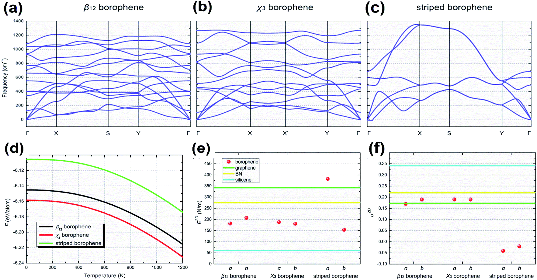 | ||
| Fig. 18 (a–c) Dispersion of phonons with different lines of symmetry for the (a) β12 phase, (b) χ3 phase, (c) striped borophene. (d) Helmholtz free energy varying with the increase in temperature for the β12 phase (black), χ3 phase (red), striped borophene (green). Comparison of (e) Young's modulus and (f) Poisson's ratio for all three phases of borophene (red dots), graphene (green line), boron nitrate (yellow line), silicene (blue line). (Reproduced from ref. 97, published by Taylor & Francis Group, licensed under Creative Common Attribution.) | ||
5.2. Thermodynamic stability
Phonons determine the relative stability of the crystal structure at 0 K as well as finite temperature via Helmholtz free energy, describing their thermodynamical stability.150 The Helmholtz free energies of stripped borophene, χ3 and β12 after including the zero-point energy at 0 K were found to be −6.106, −6.159, −6.145 eV per atom, respectively. These values were altered at higher temperatures, as shown in Fig. 18(d), for an increase in temperature between 0 K and 1000 K. Helmholtz free energy is in the order χ3 < β12 < stripped borophene, which indicates that for a wide range of temperatures, χ3 and β12 are thermodynamically very stable when compared to stripped borophene.975.3. Mechanical stability
The fulfillment of the Born–Huang criteria is essential to confirm the mechanical stability; the observed elastic constants for all three phases of borophene satisfy the criteria for Born stability,97 indicating their mechanical stability. Nevertheless, through Fig. 18(e and f), Young's modulus and Poisson's ratio were compared with the other 2D materials and it was found that the stiffness of χ3 and β12 was lower than in BN and graphene but higher than in silicene.151Furthermore, updated research on the mono- and double-doping of carbon atoms into β12, related to the resulting decrease in π-electrons, increase in σ-electrons and decrease in coordinated atoms from 4 to 6 in the double doped β12, contributed to a much better understanding of the stability.152
6. Advantages over graphene
After the synthesis of borophene, researchers have been characterizing the properties of borophene in order to find its advantages as compared to graphene and other 2-dimensional materials, and have found that borophene is stronger, more flexible, a good conductor of heat and electricity and a superconductor when compared to graphene; all these properties can also be tuned depending on the arrangement as well as the orientation of vacancies in borophene.97 Moreover, the electron-deficient behavior of boron causes the formation of borophene with multicenter bonds possessing several desirable unique physical properties.108 A much lighter, electron-rich borophene is also estimated to be an equivalent competitor of graphene due to its remarkable mechanical properties45 along with orientationally controllable properties for various applications.A theoretical analysis demonstrated that borophene with a hollow hexagon concentration of 1/6 has a bending stiffness that is twice that of graphene and even though the H–H bonds are absent in the boron sheets, they are much stronger than graphene, which makes borophene a better replacement for advancement in the composites.67 In the armchair direction, borophene with the phase Pmmm and 2-Pmmn has a much larger Young's modulus (574.61 N m−1 and 398 N m−1) when compared to that of graphene (338.08 N m−1),110 which highlights the interesting mechanical properties of borophene over graphene. Strikingly, although the interaction of H2 with borophene is similar to that of graphene, its capacity for hydrogen storage is greater than the capacity of graphene153–155 and the binding energies of gas molecules such as NO2, NO, CO2, NH3 and CO are also stronger on borophene when compared to the reports on other 2D material.156,157 Hence, borophenes are highly recommended for the detection of toxic gases, as other 2D materials including graphene lack high selectivity and sensitivity due to their zero-band gap.3
Interestingly, theoretical calculations revealed that metallic borophene sheets with an exceptional anisotropic behavior74,158 are a better conductor of electricity38,159 and possess better properties for thermal transport140 when compared to graphene. Moreover, the stability induced by the substrate on borophene frames an intermediate class of covalently bonded, templated sheets having distinct properties along with consistent structures when compared to other previously reported 2D materials.160
7. An interesting material for numerous applications
Presently, borophene is considered to be a potential material for a range of applications in various fields. Physicists are entranced by the ability of borophene as a sensor for the detection of various kinds of molecules and their atoms.133,161–164 Chemists are excited about its catalytic capability,152,165–170 and electrochemists are researching borophene as a good anode material for the generation of a better, powerful metal-ion battery.4,125,171–173 Borophene also exhibits potential in various other applications.5,38,106,174–1787.1. Biomedical applications
Borophene as a 2D nanomaterial has attracted significant attention and has been studied widely in the field of biomedicine because of its good flexibility.53 It can be considered one of the promising biomaterials since it shows different physical and chemical characteristics in its different phases, which could be heterogeneously personalized for various biomedicines as well as medical devices.106 The unstable nature of honeycomb borophene satisfies the biodegradability essential for biomedical applications.53 When combined with metals and semiconductors, borophene showed improvement in the biological applications without negative impacts.50Recent reports indicated that the sequencing of DNA is done in different ways by determining the sequence of the base, which is essential for decoding the human biological code,179,180 and several studies regarding medicine and biology have been conducted.181,182 The results of the electron sensitivity of B36 borophene towards 4 nitrogenous bases, cytosine (C), thymine (T), guanine (G) and adenine (A), over DNA showed that borophene when attached to different bases as shown in Fig. 19(a) gave different electrical signals and conductivity, as well as variations in energy and energy gap as shown in Table 2, provoking it to be used in devices for the sequencing of DNA.136
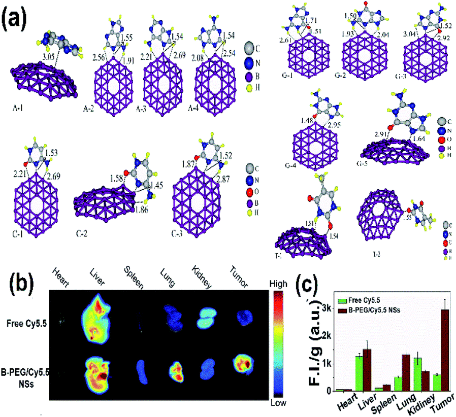 | ||
| Fig. 19 (a) Different nucleobase/B36 complexes {adenine/B36 (A-1, A-2, A-3, A-4), cytosine/B36 (C-1, C-2, C-3), thymine/B36 (T-1, T-2), guanine/B36 (G-1, G-2, G-3, G-4, G-5)} consisting of carbon (white), nitrogen (blue), oxygen (red), boron (purple), hydrogen (yellow) formed after optimization. (Reproduced from ref. 136 with the permission of Elsevier). (b) Fluorescence imaging (FI) of tumors and other organs. (c) Comparison of (FI) for bare Cy5.5 (green) and B-PEG/Cy5.5NSs (brown). (Reproduced from ref. 21, published by Wiley-VCH GmbH, Licensed under Creative Common Attribution 4.0 International). | ||
| System | Ead | EHOMO | ELUMO | Eg | ΔEg (%) |
|---|---|---|---|---|---|
| B36 | — | −5.05 | −4.01 | 1.04 | — |
| Adenine/B36-1 | −19.7 | −4.89 | −3.91 | 1.06 | +1.6 |
| Adenine/B36-2 | −39.2 | −4.37 | −3.52 | 0.86 | −17.5 |
| Adenine/B36-3 | −57.3 | −4.38 | −3.51 | 0.87 | −16.3 |
| Adenine/B36-4 | −45.5 | −4.43 | −3.60 | 0.83 | −20.2 |
| Cytosine/B36-1 | −38.1 | −4.19 | −3.49 | 0.71 | −32.0 |
| Cytosine/B36-2 | −4.8 | −3.81 | −3.77 | 0.05 | −95.5 |
| Cytosine/B36-3 | −34.7 | −4.00 | −3.69 | 0.30 | −70.9 |
| Guanine/B36-1 | −35.2 | −4.45 | −3.58 | 0.88 | −15.3 |
| Guanine/B36-2 | −43.1 | −4.67 | −3.80 | 0.88 | −15.6 |
| Guanine-3 | −37.3 | −4.04 | −3.15 | 0.88 | −14.8 |
| Guanine-4 | −22.3 | −3.98 | −3.43 | 0.54 | −47.9 |
| Guanine-5 | −20.5 | −4.15 | −3.39 | 0.76 | −26.6 |
| Thymine-1 | 4.4 | −4.31 | −3.57 | 0.74 | 28.9 |
| Thymine-2 | 10.2 | −4.27 | −3.60 | 0.67 | −35.5 |
Tumor therapy is one of the fields that has popularized nanomaterials because tumors exhibit enhanced permeability and retention (EPR) effect; drugs with sizes of 10 to 1000 nm can enrich the tumor site to passively target tumors, reduce side effects and improve efficacy.183,184 Additionally, drug delivery is more advantageous through borophene as it can make itself stable by easily combining with other groups or elements. Nonetheless, drug delivery often requires special group modification to stabilize the delivery system of the body and for the accurate release of the drug at the tumor site.185,186 As indicated in Fig. 19(b and c) the fluorescence image of the malignant tumor could be identified by easily differentiating it from that of normal tissue in the case of a tumor mouse injected with PEG-modified Cy5.5 borophene (B-PEG/Cy5.5NSs) when compared to the tumor mouse injected with bare Cy5.5.88 This promotes the application of borophene towards bioimaging, which includes photothermal imaging, photoacoustic imaging and fluorescence imaging.21
Cancer treatments can be achieved with minimal invasiveness through photothermal therapy, where NIR radiation is used to irradiate the tumor, which kills the tumor cells by increasing their temperature by photothermal conversion.187 A better therapeutic effect was observed in the case of borophene due to its UV absorbance property, and efficacy in photothermal conversion and photothermal stability; hence borophene was a potential candidate for photothermal tumor therapy.88 Furthermore, biomedical performances such as biocompatibility, targeting ability, circulation, and loading capacity can be enhanced by the appropriate functionalization or surface modification. Surface-functionalized Xenes when compared to their pristine form showed enhanced surface reactivity, stability of dispersion and invoked degradation kinetics, which minimized the toxic response and maximized the biological outcomes.188 Hence, the exfoliation of borophene after modification by PEG-NH2 (molecular weight = 2000) by powerful electrostatic adsorption, reported a layer with about 33.6% (w/w) of PEG in the resulting material. This could release a better borophene than its bare form with better dispersibility and stability, resulting in agglomeration in the cell culture medium and phosphate buffer saline,88 which could be a favorable factor for both theragnostic and therapeutic applications.188
7.2. Energy storage applications
The energy storage applications include metal-ion batteries, supercapacitors, hydrogen storage devices, solar cells, etc. Most frequently, the energy storage capacity of borophene is theoretically investigated through software simulations of molecular dynamics.176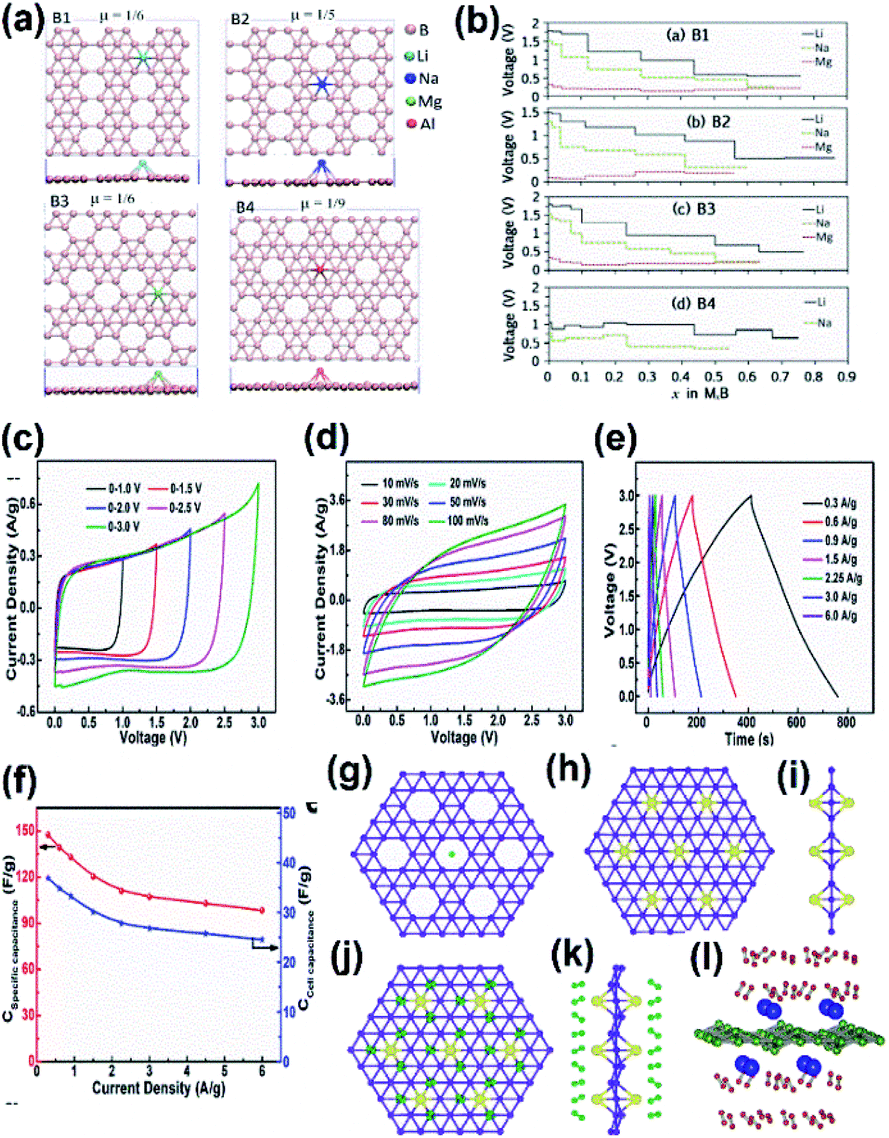 | ||
| Fig. 20 (a) Top view of borophene sheets with different hole densities (μ) and the metal atoms Li (light blue), Na (dark blue), Mg (green), Al (red) binding their favorable sites to form B1, B2, B3, B4 respectively. (b) Voltage curve of metal atom coverage for B1, B2, B3, B4 for its maximum yielding capacity. (Reproduced from ref. 173 with permission from Elsevier). (c–f) Electrolytic properties of borophene supercapacitors. (c) C–V results at different voltages. (d) C–V results at different scan rates. (e) GCD results. (f) Cell capacitance curve (blue) and specific capacitance curve (red) for varying current densities. (Reprinted (adapted) with permission from ref. 194. Copyright {2018} American Chemical Society). (g) Bare α-sheet borophene. (h) Top view and (i) side view of α-sheet borophene decorated with Li atoms (yellow). (j) Top view and (k) side view of H2 (green) adsorbed α-sheet borophene decorated with Li atoms (yellow). (Reprint (adapted) with permission from ref. 202. Copyright (2009) American Chemical Society). (l) Side view of the H2 (green) adsorbed α-sheet borophene decorated with Ca atoms (blue). (Reproduced from ref. 154 with permission from Elsevier). | ||
| Structure | Hexagonal hole density | Charge capacity (mA h g−1) | ||
|---|---|---|---|---|
| Li | Na | Mg | ||
| Buckled | 0 | 1720 | 1380 | 1960 |
| B2 | 1/5 | 2040 | 1480 | 2400 |
| B3 | 1/6 | 1980 | 1550 | 2330 |
| B1 | 1/6 | 1880 | 1640 | 2480 |
| B4 | 1/9 | 1840 | 1340 | — |
It was observed that the conductivity of the 2-Pmmn phase of borophene was very high with an enormous oxidative process, which allows a charge–discharge process without any dispersion of energy, and hence could serve as a better anode material in Li-ion batteries.105,106 Moreover, the results from the simulations of ab initio molecular dynamics revealed that the specific capacitance of lithiated borophene was 4 times higher as compared to the graphite anode and the energy barrier was much lower than that of Ti3C2, and phosphorene served as the anode material. This suggests that borophene when used as an anode for Li-ion batteries, boosts power and energy density.189 However, modifications such as stratification, hydrogenation or doping alter their interactions; i.e., a Li-ion battery hydrogenated borophene shows good performances,172 whereas the level of the stored energy is impacted in the Li–sulphide (LiS) battery when β12 and χ3 phases are introduced into it. χ3 modifies the structure of the LiS battery for the absorption of energy to avoid its structure alteration during charge–discharge cycles and the adsorption energies of Li2Sn on χ3 are 2.87, 2.53 and 2.67 for n = 8, 6 and 4 respectively, indicating it to be suitable material for anchoring over LiS batteries and although β12 adsorbs just a small amount of energy, it enhances the overall structural stability of LiS. Hence, both defective borophenes enhanced the capacity of retention and suppressed the shuttle effect, which served as excellent anchoring materials for LiS batteries.87 A LiS battery with high energy density can be realized by stabilizing the polysulphide shuttle and loading high sulphur and this can be achieved when borophene serves as a host for the sulphur cathode, due to its small deformation, high conductivity and strong adsorption.171
On considering the sodium-ion battery as an example of ultra-high theoretical capacitance,189 the potentials of two structures, namely the triangular boron layer (BΔ) and hexagonal vacancies (B⎔) were investigated by the first-principles calculations. It was observed that the adsorption energy of Na and specific capacitance for BΔ were −1.731 eV and 248 mA h g−1, respectively, and for B⎔ they were −1.448 eV and 298 mA h g−1, respectively. Moreover, the energy barrier for BΔ was just 12 meV, suggesting the extremely fast diffusion and directional anisotropy of sodium in BΔ. Along with this, the metallic characteristics observed during the sodiation process indicate an outstanding electronic conductivity and suggest that it can efficiently serve as an anode for Na-ion batteries, boosting the power density and energy of the batteries.4
Due to the small diffusion barrier with high mechanical strength and specific capacity, borophene was predicted to be a potential anode material but it was unstable without a metal substrate. Hence, to improve its stability, researchers recently proposed a new form of borophene establishing van der Waals heterostructures with graphene (B/G), and observed a high absorbance energy (−2.959 eV) and high specific capacitance (1469.35 mA h g−1), with a small specific capacitance (0.613 eV) of Li theoretically increasing the specific capacitance and decreasing the diffusion barrier to 1763 mA h g−1 and 0.353 eV, respectively, as a result of the changes made by Li on the distance of interlayers in B/G. This demonstrated B/G to be a new anode material in which its electrochemical performances could be controlled by altering the spacing of the interlayers.125
Previous studies reported that the supercapacitors consisting of borophene with multi-layers showed good results, i.e., they retained 88% of the initial capacity, even when there was a discharge of more than 6000 cycles194 it could store a huge amount of energy to serve as a promising biomedical implantable device, especially in rehabilitative robotics.195 Recent theoretical studies showed that borophene could exhibit better electrochemical performances than graphene, which made it suitable for supercapacitors. The properties include a larger voltage window with high stability (Fig. 20(c)), the CV curves were nearly rectangular even with the scan rate = 100 mV s−1 (Fig. 20(d)),194 and good capacitance behavior with fast charge–discharge rate (Fig. 20(e)). The specific capacitance was 147.6 F g−1 for 0.3 A g−1 of current density (Fig. 20(f)), and was much higher as compared to bulk boron and carbon-based materials.196–198
A very recent study on the capacitive properties through the band structures of eight sheets related to borophene revealed that among them, the Fermi levels of seven sheets consisted of Dirac cones and their carriers had higher velocity than graphene. Hence, the larger differential and integrated quantum capacitance with large charge stored at the surface make them superior electrodes for supercapacitors.174 The ultrasonic exfoliation of α-borophene and further growth into polyaniline: α borophene through electrostatic repulsion was investigated on a nickel foam substrate and it was reported that its specific capacitance was 960 F g−1 and there was 95% retention even after 1000 cycles. This indicated that α-borophene could enhance the performance of polyaniline, making it a promising material for supercapacitors.175 Thus, all the above results with remarkable features made the supercapacitance of the already existing supercapacitor more advanced when treated with borophene.
| Decorated metal atom | 2D material | Structure | Adsorption energy (eV per H2) | Hydrogen storage capacity (in wt%) | References |
|---|---|---|---|---|---|
| Li | Borophene | η = 1/8 | 0.23 | 15.26 | 207 |
| β12 | 0.22 | 10.85 | 208 | ||
| χ3 | 10.39 | 10.79 | 133 | ||
| α-sheet | 0.15 | 10.75 | 202 | ||
| η = 1/7 | 0.35 | 9.22 | 209 | ||
| 2-Pmmn | ∼0.11 | 6.8 | 210 | ||
| Graphyne | — | 0.19 | 13.0 | 211 | |
| Graphene | — | 0.21 | 12.8 | 212 | |
| Silicene | — | 0.26 | 6.35 | 204 | |
| MoS2 | — | 0.20 | 4.80 | 213 | |
| Na | Borophene | 2-Pmmn | 0.11 | 9.0 | 210 |
| α-sheet | 0.07 | 8.36 | 202 | ||
| χ-ho | 0.15 | 8.28 | 214 | ||
| Ca | Borophene | α-sheet | 0.19 | 12.68 | 154 |
| β12 | 0.24 | 9.5 | 153 | ||
| 2-Pmmn | ∼0.11 | 7.6 | 210 | ||
| χ3 | 0.23 | 7.2 | 153 | ||
| Graphyne | — | ∼0.2 | ∼7 | 215 | |
| BC7 | — | 0.26 | 4.96 | 216 | |
| K | Borophene | α-sheet | 0.06 | 2.39 | 202 |
The interaction of a single hydrogen molecule on α-borophene sheet (with adsorption energy of 0.047 eV) was found to be similar to hydrogen interaction with graphene (with adsorption energy of 0.025 eV).202 Moreover, it was observed that the storage capacity and binding energy of H2 increased when alkali-metals were dispersed on the sheet of boron (the dispersion of Li on boron and binding of H2 are represented in Fig. 20(g–k)). Among them, the boron-Li system could contain 10.7 weight% of the hydrogen molecule with 0.15 eV binding energy, indicating it to be a good template for storing hydrogen.202 In the previous study, it was observed that Ca could capture 6 hydrogen molecules at 0 K, and when both sides were adsorbed by Ca, its gravimetric density reached 12.68 wt%. Moreover, an increase in temperature along with pressure elevated the performance of hydrogen storage on borophene decorated with Ca.154
In one of the very recent research projects on the honeycomb borophene oxide, when decorated with different metals (K, Na and Li), the DFT-d2 (dispersion corrected) simulations showed that a structure of B2O decorated with Li achieved a high gravimetric density (8.3 wt% H2) theoretically, and at saturation, the binding energy of two hydrogen molecules when bound by a single Li gave a binding energy of −0.24 eV per H2. Born-Oppenheimer Molecular Dynamic (BOMD) simulation at different temperatures showed its stability along with reversibility in its binding of H2 on Li/B2O or desorption of hydrogen, which introduced a new form of borophene that could show reversibility in the hydrogen storage as well.155 Hence, various forms of borophene can be used for storing hydrogen in fuel cell equipped vehicles.
7.3. Sensors
The high mobilities of 2D materials at their monolayer thickness have attracted phosphorene, WS2, MoS2, BN and graphene towards sensing applications. However, the deficiency of the electronic bandgap in materials like graphene leads to a lack of high selectivity and sensitivity, indicating its unsuitability for the detection of toxic gases.3 However, to improve these deficiencies of 2D materials, borophene with metallic structure and enhanced electron density was introduced for vast gas sensing applications as it can adsorb several molecules of gas due to its large surface.95 In particular, it can be efficiently used as a sensor for toxic gases like NO, CO157,217 and formaldehyde,135 as well as non-toxic gases like ethanol162 and ammonia130 along with the detection of hydrogen cyanide.131 Borophenes were also considered to be suitable gas sensors after analysing the electronic and transport properties of edge-hydrogenated borophene through DFT and non-equilibrium Green's function (NEGF).133Theoretical electrochemical studies showed that easier charge transfer between the borophene nanosheets leading to the changing conductivity is one of the conditions favourable for chemical sensors and these can be observed through the band structures and DOS spectrum of borophene nanosheets.162 On considering this, the adsorption of ethanol was observed through the sharp increment in the current through borophene, indicating that it is an ethanol sensor.162 Moreover, in B36 borophene, electrical signals were generated due to the increase in its electrical conductivity after the adsorption of formaldehyde. This indicated that B36 is suitable for the construction of a formaldehyde sensor,135 and its sensitivity towards different concentrations of HCN indicates B36 to be a good sensor for toxic gases. Additionally, it has been reported that for the CO and NO sensors, all fullerenes of boron can be used.217 Further, after observing the current–voltage, transmission function and the electronic structure of the 2-Pmmn phase after the adsorption of NH3, NO2, NO and CO, it was studied as a sensor,138 and a similar phenomenon was observed in the free-standing borophene for a good ammonia sensor.93 Hence the overall results reported different phases of borophenes acting as sensors for the detection of different gasses. Along with these, the semiconductors such as MoS2 could also be used as gas sensors for NO molecules when used as substrates for the heterostructures of borophene/MoS2.161 Recently, greater efficiency as a sensor was observed in the β12 and χ3 phase when the direct micromechanical exfoliation technique was employed for their synthesis because by this method, the resulting sheets of borophene were highly crystalline, due to which there was an enhancement in the purity of chemical phase formation, necessary for an ideal sensor.103 Moreover, there are other reports on the computational studies on borophene as humidity sensors,164 metronidazole drug sensor218 and many other sensors.
7.4. Electrocatalytic applications
Borophene being the lightest 2D nanomaterial can serve as a potential catalyst in the reactions for the evolution of hydrogen (HER),165,167,169 reduction of oxygen (ORR),166 the evolution of oxygen (OER)166 as well as for the electroreduction of CO2 (CRR).128,178Borophenes show wide applications in the HER. By the method of first principles, it was predicted that borophene, consisting of a basal plane with numerous active sites and exhibiting metallic conductivity with almost free energy could explore the boron monolayers (BMs) as a promising electrocatalyst for the HER.165 In the case of the χ3 phase, where the active site is the boron atom with 5-coordinates at S2 (indicated in Fig. 21(a)), the available free energy as shown in Fig. 21(f) for the adsorption of hydrogen was found to be 0.02 eV, which is much closer to zero when compared to that of platinum165 with ΔGH = −0.09 eV (ref. 219) as well as the strong interaction of H atoms with the 2-Pmmn phase (Fig. 21(b)) was observed in borophene due to high surface activity. Moreover, the metallic band structure along with numerous active sites in the basal plane of the χ3 phase indicate its catalytic performance in HER. Similarly, for the β12 phase with a 4-coordinated boron atom as an active site, i.e., at its S1 site (indicated in Fig. 21(c)), the ΔGH was only 0.1 eV Fig. 21(f) and a small value of ΔGH was also observed in the β1 phase and α-sheet as shown in Fig. 21(g) at its S1 site and S2 sites, respectively (Fig. 21(d and e)).165 Nevertheless, all their catalytic performances were not destroyed by Ag substrates.220 Further, analysis of the effect of substrate, due to the mismatch in charge transfer and strain, showed that the HER performances were positively affected by the substrate.165
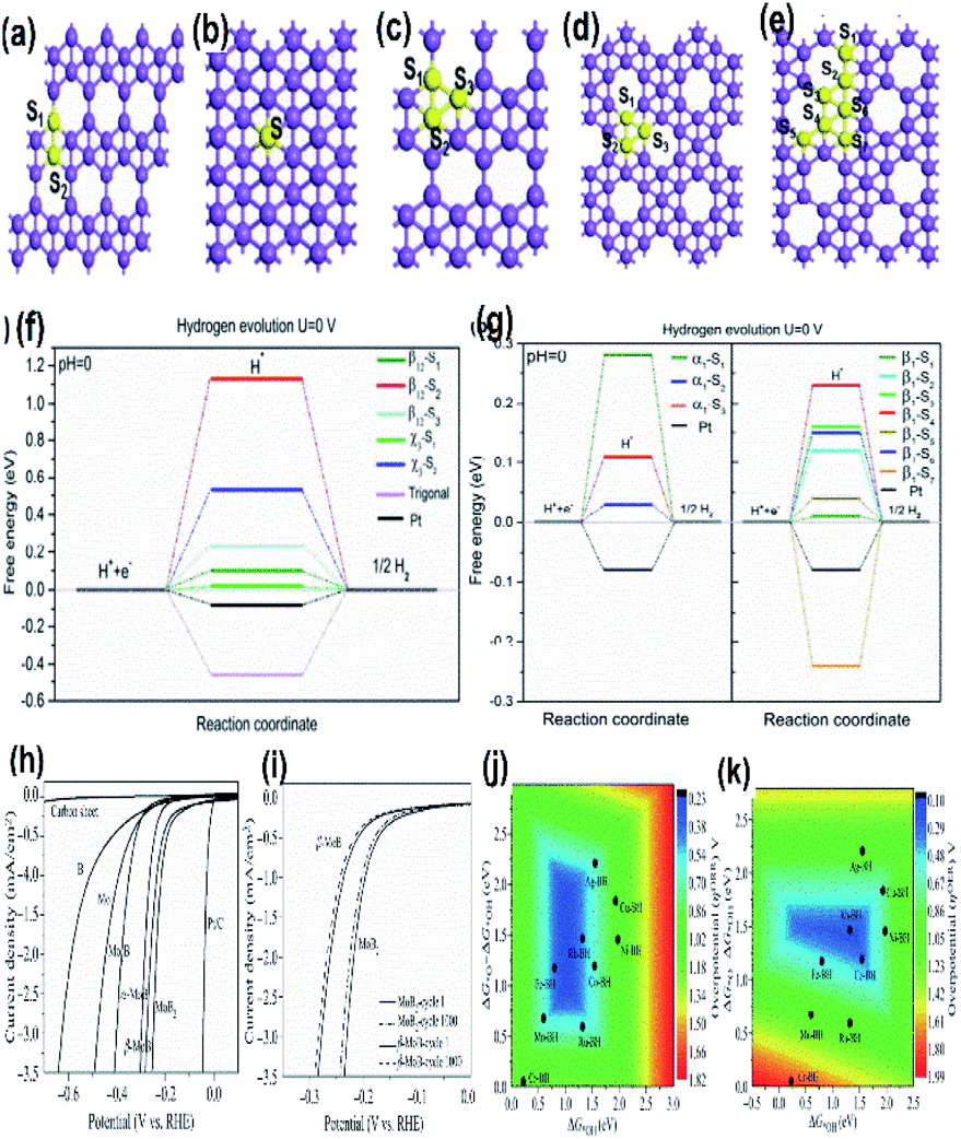 | ||
| Fig. 21 Crystal structure of the (a) χ3 phase, (b) 2-Pmmn phase, (c) β12 phase, (d) α-sheet, (e) β1 phase of borophene with purple and yellow balls indicating the B atoms. (f and g) HER free energy diagram. (Reproduced from ref. 165 with the permission of the Royal Society of Chemistry). (h) Polarization curves measured in H2SO4 (0.5 M) for Pt/C, α-MoB, MoB2, Mo, B and carbon sheet. (i) CV curves, i.e., stability measurements of MoB2 and β-MoB for the first and 1000th cycles. (Reproduced from ref. 168 with the permission of John Wiley and Sons). (j and k) Thermodynamic overpotentials of different transition metal-supported borophenes for (j) ORR activity and (k) OER activity of Gibbs free energy. (Reproduced from ref. 166 with the permission of the Royal Society of Chemistry). | ||
Furthermore, 2D sheets of boron when synthesized via chemical vapor deposition over the molybdenum foils formed an ultrathin film of molybdenum bromide (Mo3B) and showed its excellent performance as a catalyst in the reaction of hydrogen evolution (HER).167 However, as MoB2 consisted of subunits of borophene similar to that of graphene, their catalytic activities were measured with a scan rate of 1 mV s−1 for different phases of molybdenum bromide (MoB2, MoB2, α-MoB and β-MoB) in a solution of 0.5 M H2SO4. In general, the electrocatalytic performances of molybdenum and bromide are very rich when compared to that of carbon. Moreover, the four phases of molybdenum bromide are much better, with a ranking order of MoB2 > β-MoB > α-MoB > Mo2B > Mo > B, which indicates the proportionality of electrocatalytic activity with that of the amount of boron as verified from the graph of current density vs. potential in Fig. 21(h).167 The results indicated in Fig. 21(i) for the 1000th cycle in comparison with the 1st cycle revealed excellent performance as a catalyst in the hydrogen evolution reaction even after long-term cycling as compared to that of molybdenum and bromide and their performances are in the order of MoB2.167,168
A series of DFT simulations suggested that a transition metal atom supported by borophane (TM-BH) consisting of vacancies could be efficiently used as an electrocatalyst for the ORR as well as the OER and their corresponding thermodynamic potentials are represented in Fig. 21(j and k). This kind of electrocatalyst can be efficiently used for the technologies of renewable energy.166 The active reactive sites are generated for the ORR and OER due to the coupling of the transition metal d orbitals with that of the surrounding boron atoms. Among the studied TM-BH the promising electrocatalysts for the ORR were Rh–BH and Fe–BH with an overpotential of 0.47 V and 0.43 V, respectively, whereas an overpotential of 0.24 V was found for Rh–BH, indicating its suitability as an electrocatalyst for the OER.166 Further, through ab initio predictions, a study on borophene after doping with elemental dopants like lithium, sulphur, phosphorous, nitrogen and carbon also proved that the adsorption energies of oxygen and hydrogen were at the top, which subsequently suggested that doped borophene could be used as the catalyst for the evolution reactions of both oxygen and hydrogen.169 A very recent article explored the catalytic properties of vacancy-containing, carbon-doped borophene towards the OER. They discussed the role of mono-as well as dual-doping of C in β12-borophene, exploring its effect on the π and σ occupancy and reported that boron atoms deficient in charge reduced the binding of oxygen, which reduced the overpotential for the OER.152
Reduction of CO2 into hydrocarbons electrochemically promotes the usage of CO2, reducing the greenhouse effect. Practically, it is challenging to choose an ideal gas adsorbent material with good selectivity and appropriate adsorbability.53 More specifically, searching for a highly efficient, metal-free electrocatalyst for the reduction of CO2 as well as for its storage (energy storage) is still a great challenge. Nevertheless, through a DFT investigation, Qin et al.128 reported that the metallic borophene, free of metal, serves as an efficient electrocatalyst for the reduction of CO2 to CH4. The corresponding results indicated that the χ3 and β12 sheets, deficient in electrons, can be given an e− to activate CO2 by breaking the π bond. The resulting small value of the activation barrier (0.98 eV) as well as limiting potential (−0.27 V) indicated that the reduction reaction is kinetically and thermodynamically feasible.128 Further, the theoretical study along with the experiments on the electroreduction of CO2 by studying the properties of TM-β12 as a catalyst showed the stability of this boron monolayer, wherein the initial reduction products for Sc and Ti–Zn were CO and CH4 with an overpotential of 0.45 V and 0.90 V, respectively, whereas the overpotential for Fe-β12 was 0.45 V, thus revealing the reduction mechanism of CO2 via TM-β12.170 However, this was achieved even on α-borophene when doped with different metals, where the order of increase in the free energy was Co- = Fe- < Pd- < Ni- < Rh- < Ru- < Ir- < Os-doped α borophene. This indicated the very energetic reduction of CO2 on the α-borophene doped with Co and Pd when compared to the HER.177 Nevertheless, the newly designed borophene consisting of Cu chains supported on it preferably causes the electroreduction of CO2 in the following path: CO2 → COOH* → CO* → CHO* → CH2O* → CH3O* → CH3OH.178
7.5. Optical applications
The features of borophene with its capability of absorption, hybridization, optical modulation221 along with atomic layer thickness222 and excellent optical nonlinearity223 play an important role in photonic and electronic devices. It was reported that in a 2D borophene synthesized via liquid -phase exfoliation, when its nonlinear optical properties were measured through Z-scan, the observed saturable absorber (SA) properties indicated that it could serve as an excellent broadband optical switch that could be used for ultrafast mode-locking in mid-infrared and near infrared laser systems. The results further indicated that borophene could also serve as the SA in passively mode locked lasers, as well as future electro-optical applications223. Liu et al.222 used critical coupling in the visible wavelength region on the simple structure of borophene to boost the interaction of light-borophene. It was reported that the anisotropic behaviour of borophene could enhance the light absorption of the structure by 99.8% when the polarization-dependent absorption is coupled with guided resonance. The results of this mechanism also indicated that on adjusting the lifetime and carrier density of borophene, the absorption behaviour could be tuned, which could be used for future photonic and electronic devices.222 Recently, it was reported that the buckled borophene δ6 exhibits layer-dependent hyperpolarizability and optical absorption and the DFT predictions reflected the anisotropic structural characteristics, indicating the transparency with the weak absorbance of the multilayer borophene. The borophene with a non-centrosymmetric structure indicated an increase in the value of non-zero dipole hyperpolarizability with an increase in the number of layers. Hence, the integration of these properties (i.e., optics, electronics and optoelectronics) could make multi-layered borophene a promising candidate in high-performance devices.224 Zhang et al.221 found that borophene could support the surface plasmon polariton in infrared and visible regimes and hence it could integrate with numerous nanophotonic and optoelectronic devices, which could be further employed as borophene plasmon for the next-generation PoC diagnostic systems.221 Additionally, improvements in the optical and electronic properties were observed in the ionic liquid interface of hybrid borophene/graphene and this was due to the dramatic changes in the static dielectric constant as a new plasmon frequency appeared in the interface.2258. Summary and outlook
In a very short period, a new 2-dimensional allotrope of boron with much more advanced properties was predicted theoretically via DFT calculations, as well as extracted experimentally through MBE, plasma-enhanced CVD, modified Hummers' method and micromechanical exfoliation. It included both substrate-supported borophene and an independent one where all borophene phases showed interesting properties such as high mechanical properties, metallic and sensing properties, negative Poisson's ratio, conductivity and super conducting behaviour. These unique superlative properties could be further altered through strain, carrier doping, altering vacancy concentrations, the formation of heterostructures, etc. In this review, the stabilities of different structures were studied with their advantages over other 2D materials and their promising applications. The unique strategy employed by looping the theoretical and experimental results for the material design of borophene rather than direct experimental synthesis has suggested that any element and its compounds could be easily studied in the 2D form to improve the efficiency of synthesis for exploring their desirable properties and discovering new materials.Despite the advantages of the latest 2D borophene, there are many more challenges for its synthesis and practical application, as shown in Fig. 22. Although there are many theoretical suggestions regarding the properties, only a few have been experimentally confirmed because the requirement of an atmosphere with ultrahigh vacuum, and their polymorphism in 3D form limit the single-phase synthesis of borophene on a large scale. The employed growth methods are very limited and CVD being harsh and of high-cost produces materials with very small surface areas, whereas a large surface area is key for further applications. However, even though a few top-down methods like micromechanical exfoliation are simple and economical, they were unable to produce atomically layered borophene with uniform thickness. Moreover, the experimental realization of independent borophene is specifically a great challenge, as theories suggest that substrates are necessary for the crystallization of the 2D form of boron since 3D boron crystals are not a van der Waals material. However, most commonly, for their growth, the suggested substrates are metals. Since the borophene interaction is very strong with metallic substrates, a few intrinsic properties (i.e., superconductivity) of β12 and χ3 are affected and their transfer from the metal surface is also a challenging task. Moreover, the electrical shorting nature of the chosen substrate, i.e., metal, renders the transport measurements in borophene.
 | ||
| Fig. 22 Synthesis and application problems faced in general by 2D materials (reprinted with permission from ref. 3. Copyright (2020) Wiley-VCH Verlag GmbH). | ||
The rapid progress of borophene is outstanding but the efficient utilization of its high potential is yet to be confirmed. Hence, it can be summarized that along with the growing theoretical suggestions, experimental studies through the large-scale synthesis of borophene on an insulating substrate in high volume are in high demand due to the effective applications. However, conventional techniques employed in the case of graphene could also be used for the synthesis of different phases of borophene, giving rise to a final product with much more advanced properties as compared to graphene and subsequently, many more exotic properties are yet to be experimentally confirmed.
Conflicts of interest
There are no conflicts to declare.Acknowledgements
S. R. R. acknowledges the UK Engineering and Physical Sciences Research Council (EPSRC) for funding (Grant No. EP/S001395/1).Notes and references
- A. K. Geim and K. S. Novoselov, J. Nanosci. Nanotechnol., 2010, 11–19 Search PubMed.
- A. K. Geim, Phys. Scr., 2012, 2012, 014003 CrossRef.
- P. Ranjan, J. M. Lee, P. Kumar and A. Vinu, Adv. Mater., 2020, 32, 2000531 CrossRef CAS PubMed.
- P. Liang, Y. Cao, B. Tai, L. Zhang, H. Shu, F. Li, D. Chao and X. Du, J. Alloys Compd., 2017, 704, 152–159 CrossRef CAS.
- M. Novotny, F. J. D. Gutierrez and P. Krstic, J. Mater. Chem. C, 2017, 5, 5426–5433 RSC.
- X. Huang, X. Qi, F. Boey and H. Zhang, Chem. Soc. Rev., 2012, 41, 666–686 RSC.
- B. Peng, H. Zhang, H. Shao and Y. Xu, J. Mater. Chem. C, 2016, 4, 3592–3598 RSC.
- C. Huo, Z. Yan, X. Song and H. Zeng, Sci. Bull., 2015, 60, 1994–2008 CrossRef CAS.
- X. Zhang, L. Huo, A. Ciesielski and P. Samori, Adv. Energy Mater., 2016, 6, 3523 Search PubMed.
- J. Mao, Y. Wang, Z. Zheng and D. Deng, Front. Phys., 2018, 13, 1–19 CrossRef.
- C. Shang, B. Xu, X. Lei, S. Yu, D. Chen, M. Wu, B. Sun, G. Liu and C. Ouyang, Phys. Chem. Chem. Phys., 2018, 20, 20919–20926 RSC.
- C. R. Dean, A. F. Young, I. Meric, C. Lee, L. Wang, S. Sorgenfrei, K. Watanabe, T. Taniguchi, P. Kim, K. L. Shepard and J. Hone, Nat. Nanotechnol., 2010, 5, 722–726 CrossRef CAS PubMed.
- L. Li, Y. Yu, G. J. Ye, Q. Ge, X. Ou, H. Wu, D. Feng, X. H. Chen and Y. Zhang, Nat. Nanotechnol., 2014, 9, 372–377 CrossRef CAS PubMed.
- S. Zhang, Z. Yan, Y. Li, Z. Chen and H. Zeng, Angew. Chem., 2015, 127, 3155–3158 CrossRef.
- B. Feng, J. Zhang, Q. Zhong, W. Li, S. Li, H. Li, P. Cheng, S. Meng, L. Chen and K. Wu, Nat. Chem., 2000, 8, 563–568 CrossRef PubMed.
- Q. H. Wang, K. Kalantar-Zadeh, A. Kis, J. N. Coleman and M. S. Strano, Nat. Nanotechnol., 2012, 7, 699–712 CrossRef CAS PubMed.
- X.-R. Hu, J.-M. Zheng and Z.-Y. Ren, Front. Phys., 2000, 13, 1–8 Search PubMed.
- F.-f. Zhu, et al., Nat. Mater., 2015, 14, 1020–1025 CrossRef CAS PubMed.
- P. Vogt, P. D. Padova, C. Quaresima, J. Avila, E. Frantzeskakis, M. C. Asensio, A. Resta, B. Ealet and G. L. Lay, Phys. Rev. Lett., 2012, 108, 155501 CrossRef PubMed.
- J. Ji, X. Song, J. Liu, Z. Yan, C. Huo, S. Zhang, M. Su, L. Liao, W. Wang, Z. Ni, Y. Hao and H. Zeng, Nat. Commun., 2016, 7, 1–9 Search PubMed.
- M. Ou, X. Wang, L. Yu, C. Liu, W. Tao, X. Ji and L. Mei, Adv. Sci., 2021, 2001801 CrossRef CAS PubMed.
- N. R. Glavin, R. Rao, V. Varshney, E. Bianco, A. Apte, A. Roy, E. Ringe and P. M. Ajayan, Adv. Mater., 2020, 32, 1904302 CrossRef CAS PubMed.
- F. R. Fan, R. Wang, H. Zhang and W. Wu, Chem. Soc. Rev., 2021, 50, 10983–11031 RSC.
- Z. Lin, C. Wang and Y. Chai, Small, 2020, 16, 2003319 CrossRef CAS PubMed.
- S. Xie, W. Yeliang and X. Li, Adv. Mater., 2019, 31, 1900392 CrossRef PubMed.
- J. Tian, Z. Xu, C. Shen, F. Liu, N. Xu and H. Gao, Nanoscale, 2010, 2, 1375–1389 RSC.
- K. Khan, A. K. Tareen, M. Aslam, M. F. Khan, Z. Shi, C. Ma, S. S. Shams, R. Khatoon, N. Mahmood, H. Zhang and Z. Guo, Prog. Solid State Chem., 2020, 59, 100283 CrossRef CAS.
- M. Fujimori, T. Nakata, T. Nakayama, E. Nishibori, K. Kimura, M. Takata and M. Sakata, Phys. Rev. Lett., 1999, 82, 4452 CrossRef CAS.
- X. Sun, X. Liu, J. Yin, J. Yu, Y. Li, Y. Hang, X. Zhou, M. Yu, J. Li, G. Tai and W. Guo, Adv. Funct. Mater., 2017, 27, 1603300 CrossRef.
- H. Tang and S. Ismail-Beigi, Phys. Rev. Lett., 2007, 99, 115501 CrossRef PubMed.
- H. Wang, Q. Li, Y. Gao, F. Miao, X. Zho and X. G. Wan, New J. Phys., 2016, 18, 073016 CrossRef.
- A. J. Mannix, Z. Zhang, N. P. Guisinger, B. I. Yakobson and M. C. Hersam, Nat. Nanotechnol., 2018, 13, 444–450 CrossRef CAS PubMed.
- U. Alli, S. Hettiarachchi and S. Kellici, Chem.–Eur. J., 2020, 26, 6447–6460 CrossRef CAS PubMed.
- C. Liu, X. Huang, Y. Y. Wu, X. Deng, Z. Zheng, Z. Xu and D. Hu, Nanotechnol. Rev., 2021, 10, 34–49 CrossRef CAS.
- G. Forte, A. L. Magna, I. Deretzis and R. Pucci, Nanoscale Res. Lett., 2010, 5, 158–163 CrossRef CAS PubMed.
- X. Liu, Z. Zhang, L. Wang, B. I. Yakobson and M. C. Hersam, Nat. Mater., 2018, 17, 783–788 CrossRef CAS PubMed.
- Y. Huang, S. N. Shirodkar and B. I. Yakobson, J. Am. Chem. Soc., 2017, 139, 17181–17185 CrossRef CAS PubMed.
- L. Adamska, S. Sadasivam, J. J. Foley, P. Darancet and S. Sharifzadeh, J. Phys. Chem. C, 2018, 122, 4037–4045 CrossRef CAS.
- X. Zhou, X. Dong, A. R. Oganov, Q. Zhu, Y. Tian and H. Wang, Phys. Rev. Lett., 2014, 112, 085502 CrossRef.
- H. Zhou, Y. Cai, G. Zhang and Y. Zhang, npj 2D Mater. Appl., 2017, 1, 1–7 CrossRef.
- H. Zhong, K. Huang, G. Yu and S. Yuan, Phys. Rev. B, 2018, 98, 054104 CrossRef CAS.
- A. Mogulkoc, Y. Mogulkoc, D. Kecik and E. Durgun, Phys. Chem. Chem. Phys., 2018, 20, 21043–21050 RSC.
- L. Xu, A. Du and L. Kou, Phys. Chem. Chem. Phys., 2016, 18, 27284–27289 RSC.
- X. Liu and M. C. Hersam, Sci. Adv., 2019, 5, eaax6444 CrossRef CAS PubMed.
- A. J. Mannix, X. Zhou, B. Kiraly, J. D. Wood, D. Alducin, B. D. Myers, X. Liu, B. L. Fisher, U. Santiago, J. R. Guest, M. J. Yacaman, A. Ponce, A. R. Oganov, M. C. Hersam and N. P. Guisinger, Science, 2015, 350, 1513–1516 CrossRef CAS PubMed.
- X. Zhang, H. Xie, M. Hu, H. Bao, S. Yue, G. Qin and G. Su, Phys. Rev. B: Condens. Matter Mater. Phys., 2014, 89, 054310 CrossRef.
- I. Boustani, Phys. Rev. B: Condens. Matter Mater. Phys., 1997, 55, 16426 CrossRef CAS.
- I. Boustani, Chem. Phys. Lett., 1995, 240, 135–140 CrossRef CAS.
- I. Boustani, Surf. Sci., 1997, 370, 355–363 CrossRef CAS.
- Z. A. Piazza, H. Hu, W. Li, Y. Zhao, J. Li and L. Wang, Nat. Commun., 2014, 5, 1–6 Search PubMed.
- W. Li, L. Kong, C. Chen, J. Gou, S. Sheng, W. Zhang, H. Li, L. Chen, P. Cheng and K. Wu, Sci. Bull., 2018, 63, 282–286 CrossRef CAS.
- A. L. Robinson, MRS Bull., 2017, 42, 337–338 CrossRef.
- Z. Xie, X. Meng, X. Li, W. Liang, W. Huang, K. Chen, J. Chen, C. Xing, M. Qiu, B. Zhang, G. Nie, N. Xie, X. Yan and H. Zhang, Research, 2020, 2020, 2624617 CrossRef CAS PubMed.
- C. Hou, G. Tai, Z. Wu and J. Hao, ChemPlusChem, 2020, 85, 2186–2196 CrossRef CAS PubMed.
- I. Boustani, J. Solid State Chem., 1997, 133, 182–189 CrossRef CAS.
- A. Quandt and I. Boustani, ChemPhysChem, 2005, 6, 2001–2008 CrossRef CAS PubMed.
- A. Gindulytė, W. N. Lipscomb and L. Massa, Inorg. Chem., 1998, 37, 6544–6545 CrossRef PubMed.
- I. Matsuda and K. Wu, 2D Boron: Boraphene, Borophene, Boronene, Springer, 2021 Search PubMed.
- K. C. Lau and R. Pandey, J. Phys. Chem. C, 2007, 111, 2906–2912 CrossRef CAS.
- D. Li, J. Gao, P. Cheng, J. He, Y. Yin, Y. Hu, L. Chen, Y. Cheng and J. Zhao, Adv. Funct. Mater., 2020, 30, 1904349 CrossRef CAS.
- I. Boustani, A. Quandt, E. Hernandez and A. Rubio, J. Chem. Phys., 1999, 110, 3176–3185 CrossRef CAS.
- D. Y. Zubarev and A. I. Boldyrev, Science and Technology of Atomic Molecular, Condensed Matter & Biological Systems Book Series, 2010, 219–267 Search PubMed.
- X. Yang, Y. Ding and J. Ni, Phys. Rev. B: Condens. Matter Mater. Phys., 2008, 77, 041402 CrossRef.
- K. C. Lau, R. Pati, R. Pandey and A. C. Pineda, Chem. Phys. Lett., 2006, 418, 1105–1110 CrossRef.
- I. Cabria, J. A. Alonso and M. J. López, Phys. Status Solidi A, 2006, 203, 3523 CrossRef.
- H. Tang and S. Ismail-Beigi, Phys. Rev. B: Condens. Matter Mater. Phys., 2009, 80, 134113 CrossRef.
- Z. Zhang, Y. Yang, E. S. Penev and B. I. Yakobson, Adv. Funct. Mater., 2017, 27, 1605059 CrossRef.
- X. Yu, L. Li, X. W. Xu and C. C. Tang, J. Phys. Chem. C, 2012, 116, 20075–20079 CrossRef CAS.
- C. Ozdogan, S. Mukhopadhyay, W. Hayami, Z. B. Guvenc, R. Pandey and I. Boustani, J. Phys. Chem. C, 2010, 114, 4362–4375 CrossRef CAS.
- Y. Zhao, S. Zeng and J. Ni, Appl. Phys. Lett., 2016, 108, 242601 CrossRef.
- T. R. Galeev, Q. Chen, J. C. Guo, H. Bai, C. Q. Miao, H. G. Lu, A. P. Sergeeva and A. I. Boldyrev, Phys. Chem. Chem. Phys., 2011, 13, 11575–11578 RSC.
- E. S. Penev, S. Bhowmick, A. Sadrzadeh and B. I. Yakobson, Nano Lett., 2012, 12, 2441–2445 CrossRef CAS PubMed.
- Y. Wang, J. Lv, L. Zhu and Y. Ma, Phys. Rev. B: Condens. Matter Mater. Phys., 2010, 82, 094116 CrossRef.
- X. Wu, j. Dai, Y. Zhao, Z. Zhuo, J. Yang and X. C. Zeng, ACS Nano, 2012, 6, 7443–7453 CrossRef CAS PubMed.
- G. P. Campbell, A. J. Mannix, J. D. Emery, T. L. Lee, N. P. Guisinger, M. C. Hersam and M. J. Bedzyk, Nano Lett., 2018, 18, 2816–2821 CrossRef CAS PubMed.
- Y. Jiao, F. Ma, J. Bell, A. Bilic and A. Du, Angew. Chem., 2016, 128, 10448–10451 CrossRef.
- Z. Zhang, E. S. Penev and B. I. Yakobson, Chem. Soc. Rev., 2017, 46, 6746–6763 RSC.
- L. Kong, K. Wu and L. Chen, Front. Phys., 2018, 13, 1–11 CrossRef CAS.
- Y. Zhao, S. Zeng and J. Ni, Phys. Rev. B, 2016, 93, 014502 CrossRef.
- Y. Liu, E. S. Penev and B. I. Yakobson, Angew. Chem., Int. Ed., 2013, 52, 3156–3159 CrossRef CAS PubMed.
- Z. Zhang, Y. Yang, G. Gao and B. I. Yakobson, Angew. Chem., 2015, 127, 13214–13218 CrossRef.
- H. Liu, J. Gao and J. Zhao, Sci. Rep., 2013, 3, 1–9 Search PubMed.
- S. Xu, Y. Zhao, J. Liao, X. Yang and H. Xu, Nano Res., 2016, 9, 2616–2622 CrossRef CAS.
- Z. Zhang, S. N. Shirodkar, Y. Yang and B. I. Yakobson, Angew. Chem., 2017, 129, 15623–15628 CrossRef.
- Y. Yao, F. Ye, X. L. Qi, S. C. Zhang and Z. Fang, Phys. Rev. B: Condens. Matter Mater. Phys., 2007, 75, 041401 CrossRef.
- A. N. Kolmogorov and S. Curtarolo, Phys. Rev. B: Condens. Matter Mater. Phys., 2006, 74, 224507 CrossRef.
- H. R. Jiang, W. Shyy, M. Liu, Y. X. Ren and T. S. Zhao, J. Mater. Chem. A, 2018, 6, 2107–2114 RSC.
- X. Ji, N. Konh, J. Wang, W. Li, Y. Xiao, S. T. Gan, Y. Zhang, Y. Li, X. Song, Q. Xiong, S. Shi, Z. Li, W. Tao, H. Zhang, L. Mei and J. Shi, Adv. Mater., 2018, 30, 1803031 CrossRef PubMed.
- J. N. Coleman, Acc. Chem. Res., 2013, 46, 14–22 CrossRef CAS PubMed.
- Z. Wu, G. Tai, W. Shao, R. Wang and C. Hou, Nanoscale, 2020, 12, 3787–3794 RSC.
- Z. Yan, Z. Peng and J. M. Tour, Acc. Chem. Res., 2014, 47, 1327–1337 CrossRef CAS PubMed.
- G. Tai, T. Hu, Y. Zhou, X. Wang, J. Kong, T. Zeng, Y. You and Q. Wang, Angew. Chem., Int. Ed., 2015, 54, 15473–15477 CrossRef CAS PubMed.
- P. Ranjan, T. K. Sahu, R. Bhushan, S. S. R. K. C. Yamijala, D. J. Late, P. Kumar and A. Vinu, Adv. Mater., 2019, 31, 1900353 CrossRef PubMed.
- L. Zhu, B. Zhao, T. Zhang, G. Chen and S. A. Yang, J. Phys. Chem. C, 2019, 123, 14858–14864 CrossRef CAS.
- B. Kiraly, X. Liu, L. Wang, Z. Zhang, A. J. Mannix, B. L. Fisher, B. I. Yakobson, M. C. Hersam and N. P. Guisinger, ACS Nano, 2019, 13, 3816–3822 CrossRef CAS PubMed.
- R. Wu, A. Gozar and I. Božović, npj Quantum Mater., 2019, 4, 1–6 CrossRef CAS.
- B. Peng, H. Zhang, H. Shao, Z. Ning, Y. Xu, G. Ni, H. Lu, D. W. Zhang and H. Zhu, Mater. Res. Lett., 2017, 5, 399–407 CrossRef CAS.
- Z. Wu, G. Tai, R. Liu, C. Hou, W. Shao, X. Liang and Z. Wu, ACS Appl. Mater. Interfaces, 2021, 13, 31808–31815 CrossRef CAS PubMed.
- K. M. Omambac, M. Petrovic, P. Bampoulis, C. Brand, M. A. Kriegel, P. Dreher, D. Janoschka, U. Hagemann, N. Hartmann, P. Valerius, T. Michely, F. J. M. Zu Heringdorf and M. H. Hoegen, ACS Nano, 2021, 15, 7421–7429 CrossRef CAS PubMed.
- N. A. Vinogradov, A. Lyalin, T. Taketsugu, A. S. Vinogradov and A. Preobrajenski, ACS Nano, 2019, 13, 14511–14518 CrossRef CAS PubMed.
- W. Choi, I. Lahiri, R. Seelaboyina and Y. S. Kang, Crit. Rev. Solid State Mater. Sci., 2010, 35, 52–71 CrossRef CAS.
- M. Khalkhali, A. Rajabpour and F. Khoeini, Sci. Rep., 2019, 9, 1–12 CAS.
- S. Chahal, P. Ranjan, M. Motlag, S. S. R. K. C. Yamijala, D. J. Late, E. H. S. Sadki, G. J. Cheng and P. Kumar, Adv. Mater., 2021, 33, 2102039 CrossRef CAS PubMed.
- T. C. Lebepe, P. Sundararajan and S. O. Oluwatobi, Nanomaterials, 2020, 10, 2149 CrossRef CAS PubMed.
- D. Ayodhya and G. Veerabhadram, FlatChem, 2020, 19, 100150 CrossRef CAS.
- M. Tatullo, B. Zavan, F. Genovese, B. Codispoti, I. Makeeva, S. Rengo, L. Fortunato and G. Spagnuolo, Appl. Sci., 2019, 9, 3446 CrossRef CAS.
- G. I. Giannopoulos, Comput. Mater. Sci., 2017, 129, 304–310 CrossRef CAS.
- B. Mortazavi, O. Rahaman, A. Dianat and T. Rabczuk, Phys. Chem. Chem. Phys., 2016, 18, 27405–27413 RSC.
- V. Wang and W. T. Geng, J. Phys. Chem. C, 2017, 121, 10224–10232 CrossRef CAS.
- Z. Q. Wang, T. Y. Lu, H. Q. Wang, Y. P. Feng and J. C. Zheng, Front. Phys., 2019, 14, 1–20 Search PubMed.
- Z. Wang, T. Y. Lu, H. Q. Wang, Y. P. Feng and J. C. Zheng, Phys. Chem. Chem. Phys., 2016, 18, 31424–31430 RSC.
- R. Peköz, M. Konuk, M. E. Kilic and E. Durgun, ACS Omega, 2018, 3, 1815–1822 CrossRef PubMed.
- J. He, D. Li, Y. Ying, C. Feng, J. He, C. Zhong, H. Zhou, P. Zhou and G. Zhang, npj Comput. Mater., 2019, 5, 1–8 CrossRef CAS.
- C. Hou, G. Tai, J. Hao, L. Sheng, B. Liu and Z. Wu, Angew. Chem., 2020, 132, 10911–10917 CrossRef.
- Q. Wei and X. Peng, Appl. Phys. Lett., 2014, 104, 251915 CrossRef.
- J. H. Liao, Y. C. Zhao, Y. J. Zhao, H. Xu and X. B. Yang, Phys. Chem. Chem. Phys., 2017, 19, 29237–29243 RSC.
- H. Liu, A. T. Neal, Z. Zhu, Z. Luo, X. Xu, D. Tománek and P. D. Ye, ACS Nano, 2014, 8, 4033–4041 CrossRef CAS PubMed.
- J. Kunstmann and A. Quandt, Phys. Rev. B: Condens. Matter Mater. Phys., 2006, 74, 035413 CrossRef.
- I. Boustani and A. Quandt, Comput. Mater. Sci., 1998, 11, 132–137 CrossRef CAS.
- Y. Wang, X. Jiang, Y. Wang and J. Zhao, Phys. Chem. Chem. Phys., 2021, 23, 17150–17157 RSC.
- W. Shao, G. Tai, C. Hou, Z. Wu, Z. Wu and X. Liang, ACS Appl. Electron. Mater., 2021, 3, 1133–1141 CrossRef CAS.
- W. Hu, N. Qin, G. Wu, Y. Lin, S. Li and D. Bao, J. Am. Chem. Soc., 2012, 134, 14658–14661 CrossRef CAS PubMed.
- Z. Q. Wang, T. Y. Lu, H. Q. Wang, Y. P. Feng and J. C. Zheng, RSC Adv., 2017, 7, 47746–47752 RSC.
- Y. Zhang, Z. F. Wu, P. F. Gao, S. Zhang and Y. H. Wen, ACS Appl. Mater. Interfaces, 2016, 8, 22175–22181 CrossRef CAS PubMed.
- J. Yu, M. Zhou, M. Yang, Q. Yang, Z. Zhang and Y. Zhang, ACS Appl. Energy Mater., 2020, 3, 11699–11705 CrossRef CAS.
- J. Khanifaev, R. Pekoz, M. Konuk and E. Durgun, Phys. Chem. Chem. Phys., 2017, 19, 28963–28969 RSC.
- J. Li, X. Chen, Z. Yang, X. Liu and X. Zhang, J. Mater. Chem. C, 2021, 9, 1069–1076 RSC.
- Q. Sun, G. Qin, Q. Cui and A. Du, ChemCatChem, 2020, 12, 1483–1490 CrossRef.
- H. Kim and H. N. Alshareef, ACS Mater. Lett., 2019, 2, 55–70 CrossRef.
- Z. Rostami and H. Soleymanabadi, J. Mol. Model., 2016, 22, 70 CrossRef PubMed.
- O. Akbar, Comput. Theor. Chem., 2017, 1115, 179–184 CrossRef.
- D. O. Lindroth and P. Erhart, Phys. Rev. B, 2016, 94, 115205 CrossRef.
- V. Shukla, J. Warna, N. K. Jena, A. Grigoriev and R. Ahuja, J. Phys. Chem. C, 2017, 121, 26869–26876 CrossRef CAS.
- T. Liu, Y. Chen, M. Zhang, L. Yuan, C. Zhang, J. Wang and J. Fan, AIP Adv., 2017, 7, 125007 CrossRef.
- A. S. Kootenaei and G. Ansari, Phys. Lett. A, 2016, 380, 2664–2668 CrossRef.
- A. Rastgou, H. Soleymanabadi and A. Bodaghi, Microelectron. Eng., 2017, 169, 9–15 CrossRef CAS.
- A. Lherbier, A. R. Botello-Méndez and J. C. Charlier, 2D Materials, 2016, 3, 045006 CrossRef.
- C. S. Huang, A. Murat, V. Babar, E. Montes and U. Schwingenschlogl, J. Phys. Chem. C, 2018, 122, 14665–14670 CrossRef CAS.
- S. Kumar, M. Singh, D. K. Sharma and S. Aulucl, Comput. Condens. Matter, 2020, 22, e00436 CrossRef.
- H. Sun, Q. Li and X. G. Wan, Phys. Chem. Chem. Phys., 2016, 18, 14927–14932 RSC.
- Y. Hu, Y. Yin, S. Li, H. Zhou, D. Li and G. Zhang, Nano Lett., 2020, 20, 7619–7626 CrossRef CAS PubMed.
- B. Mortazavi, M. Q. Le, T. Rabczuk and L. F. C. Pereira, Phys. E, 2017, 93, 202–207 CrossRef CAS.
- B. Y. Shapiro, I. Shapiro, D. Li and B. Rosenstein, J. Phys.: Condens. Matter, 2018, 30, 335403 CrossRef PubMed.
- J. Chapman, Y. Su, C. A. Howard, D. Kundys, A. N. Grigorenko, F. Guinea, A. K. Geim, I. V. Grigorieva and R. R. Nair, Sci. Rep., 2016, 6, 1–6 CrossRef PubMed.
- E. S. Penev, A. Kutana and B. I. Yakobson, Nano Lett., 2016, 16, 2522–2526 CrossRef CAS PubMed.
- J. C. Zheng and Y. Zhu, Phys. Rev. B: Condens. Matter Mater. Phys., 2006, 73, 024509 CrossRef.
- R. C. Xiao, D. F. Shao, W. J. Lu, H. Y. Lv, J. Y. Li and Y. P. Sun, Appl. Phys. Lett., 2016, 109, 122604 CrossRef.
- Y. Wang, Y. Park, L. Qiu, I. Mitchell and F. Ding, J. Phys. Chem. Lett., 2020, 11, 6235–6241 CrossRef CAS PubMed.
- R. R. Zope and T. Baruah, Chem. Phys. Lett., 2011, 501, 193–196 CrossRef CAS.
- M. J. van Setten, M. A. Uijttewaa, G. A. de Wijs and R. A. de Groot, J. Am. Chem. Soc., 2007, 129, 2458–2465 CrossRef CAS PubMed.
- R. C. Andrew, R. E. Mapasha, A. M. Ukpong and N. Chetty, Phys. Rev. B: Condens. Matter Mater. Phys., 2012, 85, 125428 CrossRef.
- E. S. Erakulan and R. Thapa, Appl. Surf. Sci., 2022, 574, 151613 CrossRef.
- X. Chen, L. Wang, W. Zhang, J. Zhang and Y. Yuan, Int. J. Hydrogen Energy, 2017, 42, 20036–20045 CrossRef CAS.
- J. Wang, Y. Du and L. Sun, Int. J. Hydrogen Energy, 2016, 41, 5276–5283 CrossRef CAS.
- P. Habibi, T. J. H. Vlugt, P. Dey and O. A. Moultos, ACS Appl. Mater. Interfaces, 2021, 13, 43233–43240 CrossRef CAS PubMed.
- L. Kou, T. Frauenheim and C. Chen, J. Phys. Chem. Lett., 2014, 5, 2675–2681 CrossRef CAS PubMed.
- O. Leenaerts, B. Partoens and F. M. Peeters, Phys. Rev. B: Condens. Matter Mater. Phys., 2008, 77, 125416 CrossRef.
- B. Feng, J. Zhang, R. Y. Liu, T. Iimori, C. Lian, H. Li, L. Chen, K. Wu, S. Meng, F. Komori and I. Matsuda, Phys. Rev. B, 2016, 94, 041408 CrossRef.
- Y. An, J. Jiao, Y. Hou, H. Wang, D. Wu, T. Wang, Z. Fu, G. Xu and R. Wu, Phys. Chem. Chem. Phys., 2018, 20, 21552–21556 RSC.
- B. Feng, Z. Ding, S. Meng, Y. Yao, X. He, P. Cheng, L. Chen and K. Wu, Nano Lett., 2012, 12, 3507–3511 CrossRef CAS PubMed.
- J. Shen, Z. Yang, Y. Wang, L. C. Xu, R. Liu and X. Liu, Appl. Surf. Sci., 2020, 504, 144412 CrossRef CAS.
- V. Nagarajan and R. Chandiramouli, Comput. Theor. Chem., 2017, 1105, 52–60 CrossRef CAS.
- M. Z. M. Nasir and M. Pumera, TrAC, Trends Anal. Chem., 2019, 121, 115696 CrossRef.
- C. Hou, G. Tai, B. Liu, Z. Wu and Y. Yin, Nano Res., 2020, 1–8 Search PubMed.
- L. Shi, C. Ling, Y. Ouyang and J. Wang, Nanoscale, 2017, 9, 533–537 RSC.
- Y. Singh, S. Back and Y. Jung, Phys. Chem. Chem. Phys., 2018, 20, 21095–21104 RSC.
- X. Wang, G. Tai, Z. Wu, T. Hu and R. Wang, J. Mater. Chem. A, 2017, 5, 23471–23475 RSC.
- H. Park, A. Encinas, J. P. Scheifers, Y. Zhang and B. P. Fokwa, Angew. Chem., Int. Ed., 2017, 56, 5575–5578 CrossRef CAS PubMed.
- S. H. Mir, S. Chakraborty, P. C. Jha, J. Warna, H. Soni, P. K. Jha and R. Ahuja, Appl. Phys. Lett., 2016, 109, 053903 CrossRef.
- J. H. Liu, L. M. Yang and E. Ganz, RSC Adv., 2019, 9, 27710–27719 RSC.
- L. Zhang, P. Liang, H. Shu, X. L. Man, F. Li, J. Huang, Q. Dong and D. Chao, J. Phys. Chem. C, 2017, 121, 15549–15555 CrossRef CAS.
- M. Makaremi, B. Mortazavi and C. V. Singh, Mater. Today Energy, 2018, 8, 22–28 CrossRef.
- B. Mortazavi, O. Rahaman, S. Ahzi and T. Rabczuk, Appl. Mater. Today, 2017, 8, 60–67 CrossRef.
- Z. L. Lv, H. L. Cui, H. Wang and X. H. Li, Appl. Surf. Sci., 2021, 562, 150154 CrossRef CAS.
- S. Göktuna and N. Taşaltın, Phys. E, 2021, 134, 114833 CrossRef.
- O. Folorunso, Y. Hamam, R. Sadiku, S. S. Ray and G. J. Adekoya, FlatChem, 2021, 26, 100211 CrossRef CAS.
- X. Xu, X. Hou, J. Lu, P. Zhang, B. Xiao and J. Mi, J. Phys. Chem. C, 2020, 124, 24156–24163 CrossRef CAS.
- H. Shen, Y. Li and Q. Sun, Nanoscale, 2018, 10, 11064–11071 RSC.
- H. S. Kim and Y. H. Kim, Biosens. Bioelectron., 2015, 69, 186–198 CrossRef CAS PubMed.
- M. Raoof, K. Jans, G. Bryce, S. Ebrahim, L. Lagae and A. Witvrouw, Microelectron. Eng., 2013, 111, 421–424 CrossRef CAS.
- A. M. Attaran, S. A. Manafi, M. Javanbakht and M. Enhessari, J. Nanostruct. Chem., 2016, 6, 121–128 CrossRef.
- A. L. Petranovska, N. V. Abramov, S. P. Turanska, P. P. Gorbyk, A. N. Kaminskiy and N. V. Kusyak, J. Nanostruct. Chem., 2015, 3, 275–285 CrossRef.
- J. Fang, H. Nakamura and H. Maeda, Adv. Drug Delivery Rev., 2011, 63, 136–151 CrossRef CAS PubMed.
- K. Bhise, S. K. Kashaw, S. Sau and A. K. Iyer, Int. J. Pharm., 2017, 526, 1–2 CrossRef PubMed.
- M. Fan, Y. Wen, D. Ye, Z. Jin, P. Zhao, D. Chen, X. Lu and Q. He, Adv. Healthcare Mater., 2019, 8, 1970054 CrossRef.
- H. Nishino, T. Fujita, A. Yamamoto, T. Fujimori, A. Fujino, S. I. Ito, J. Nakamura, H. Hosono and T. Kondo, J. Phys. Chem. C, 2017, 121, 10587–10593 CrossRef CAS.
- N. K. Prasad, K. Rathinasamy, D. Panda and D. Bahadur, J. Mater. Chem., 2007, 17, 5042–5051 RSC.
- W. Tao, N. Kong, X. Ji, Y. Zhang, A. Sharma, J. Ouyang, B. Qi, J. Wang, N. Xie, C. Kang, H. Zhang, O. C. Farokhzad and J. S. Kim, Chem. Soc. Rev., 2019, 48, 2891–2912 RSC.
- H. R. Jiang, Z. Lu, M. C. Wu, F. Ciucci and T. S. Zhao, Nano Energy, 2016, 23, 97–104 CrossRef.
- C. Liu, F. Li, L. P. Ma and H. M. Cheng, Adv. Mater., 2010, 22, E28–E62 CrossRef CAS PubMed.
- J. Yan, Q. Wang, T. Wei and Z. Fan, Adv. Energy Mater., 2014, 4, 1300816 CrossRef.
- Y. Han, Y. Ge, Y. Chao, C. Wang and G. G. Wallance, J. Energy Chem., 2018, 27, 57–72 CrossRef.
- C. Lu, Y. Yang and X. Chen, Nano Lett., 2019, 19, 4103–4111 CrossRef CAS PubMed.
- H. Li, L. Jing, W. Liu, J. Lin, R. Y. Tay, S. H. Tsang and E. H. T. Teo, ACS Nano, 2018, 12, 1262–1272 CrossRef CAS PubMed.
- P. Kerativitayanan, M. Tatullo, M. Khariton, P. Joshi, B. Perniconi and A. K. Gaharwar, ACS Biomater. Sci. Eng., 2017, 3, 590–600 CrossRef CAS PubMed.
- D. Y. Yeom, W. Jeon, N. D. K. Tu, S. Y. Yeo, S. S. Lee, B. J. Sung, H. Chang, J. A. Lim and H. Kim, Sci. Rep., 2015, 5, 1–10 Search PubMed.
- S. Saha, M. Jana, P. Khanra, P. Samanta, H. Y. Koo, N. C. Murmu and T. Kuila, ACS Appl. Mater. Interfaces, 2015, 7, 14211–14222 CrossRef CAS PubMed.
- T. Wu, X. Wu, L. Li, M. Hao, G. Wu, T. Zhang and S. Chen, Angew. Chem., Int. Ed., 2020, 59, 23800–23809 CrossRef CAS PubMed.
- R. Coontz and B. Hanson, Science, 2004, 305, 957 CrossRef CAS.
- L. Schlapbach, and A. Züttel, Materials for sustainable energy: a collection of peer-reviewed research and review articles from nature publishing group, 2011, pp. 265–270 Search PubMed.
- Y. Wang, J. Fan and M. Trenary, Chem. Mater., 1993, 5, 192–198 CrossRef CAS.
- S. Er, G. A. de Wijs and G. Brocks, J. Phys. Chem. C, 2009, 113, 18962–18967 CrossRef CAS.
- A. Lebon, R. H. Aguilera-del-Toro, L. J. Gallego and A. Vega, Int. J. Hydrogen Energy, 2019, 44, 1021–1033 CrossRef CAS.
- L. Yuan, L. Kang, Y. Chen, D. Wang, J. Gong, C. Wang, M. Zhang and X. Wu, Appl. Surf. Sci., 2018, 434, 843–849 CrossRef CAS.
- V. Tozzini and V. Pellegrini, Phys. Chem. Chem. Phys., 2013, 15, 80–89 RSC.
- J. Shang, Y. Ma, Y. Gu and L. Kou, Phys. Chem. Chem. Phys., 2018, 20, 28964–28978 RSC.
- J. Li, H. Zhang and G. Yang, J. Phys. Chem. C, 2015, 119, 19681–19688 CrossRef CAS.
- T. Liu, Y. Chen, H. Wang, M. Zhang, L. Yuan and C. Zhang, Materials, 2017, 10, 1399 CrossRef PubMed.
- Y. S. Wang, F. Wang, M. Li, B. Xu, Q. Sun and Y. Jia, Appl. Surf. Sci., 2012, 258, 8874–8879 CrossRef CAS.
- S. Haldar, S. Mukherjee and C. V. Singh, RSC Adv., 2018, 8, 20748–20757 RSC.
- B. Xu, X. L. Lei, G. Liu, M. S. Wu and C. Y. Ouyang, Int. J. Hydrogen Energy, 2014, 39, 17104–17111 CrossRef CAS.
- C. Ataca, E. Akturk, S. Ciraci and H. Ustunel, Appl. Phys. Lett., 2008, 93, 043123 CrossRef.
- C. Zhang, S. Tang, M. Deng and Y. Du, Chin. Phys. B, 2018, 27, 066103 CrossRef.
- Y. F. Zhang and X. L. Cheng, Phys. E, 2019, 107, 170–176 CrossRef CAS.
- H. J. Hwang, Y. Kwon and H. Lee, J. Phys. Chem. C, 2012, 116, 20220–20224 CrossRef CAS.
- X. L. Lei, G. Liu, M. S. Wu, B. Xu, C. Y. Ouyang and B. C. Pan, Int. J. Hydrogen Energy, 2014, 39, 2142–2148 CrossRef CAS.
- R. Chandiramouli and V. Nagarajan, Vacuum, 2017, 142, 13–20 CrossRef CAS.
- C. Xiao, K. Ma, G. Cai, X. Zhang and E. Vessally, J. Mol. Graphics Modell., 2020, 96, 107539 CrossRef CAS PubMed.
- J. K. Nørskov, T. Bligaard, A. Logadottir, J. R. Kitchin, J. G. Chen, S. Pandelov and U. Stimming, J. Electrochem. Soc., 2005, 152, J23 CrossRef.
- C. Liu, Z. Dai, J. Zhang, Y. Jin, D. Li and C. Sun, J. Phys. Chem. C, 2018, 122, 19051–19055 CrossRef CAS.
- J. Zhang, Z. Zhang, X. Song, H. Zhang and J. Yang, Nanomaterials, 2021, 11, 1165 CrossRef CAS PubMed.
- T. Liu, C. Zhou and S. Xiao, Opt. Express, 2021, 29, 8941–8950 CrossRef PubMed.
- C. Ma, P. Yin, K. Khan, A. K. Tareen, R. Huang, J. Du, Y. Zhang, Z. Shi, R. Cao, S. Weiand and X. Wang, Small, 2021, 17, 2006891 CrossRef CAS PubMed.
- G. Sachdeva, S. Kaur, R. Pandey and S. P. Karna, Computation, 2021, 9, 101 CrossRef CAS.
- K. Zhour, J. M. Otero-Mato, F. E. H. Hassan, H. Fahs, M. Vaezzadeh, E. López-Lago, L. J. Gallego and L. M. Varela, J. Mol. Liq., 2021, 321, 114759 CrossRef CAS.
| This journal is © The Royal Society of Chemistry 2022 |