
 Open Access Article
 This Open Access Article is licensed under a Creative Commons Attribution-Non Commercial 3.0 Unported Licence
Optoelectronic properties and interfacial interactions of two-dimensional Cs2PbX4–MSe2 (M = Mo, W) heterostructures
Ying Jie Chenab,
Xue Lib,
Bao Nan Jiab,
Chao Dongb,
Xiao Ning Guan *bd,
Xin Zhaoa and
Li Hong Han*abc
*bd,
Xin Zhaoa and
Li Hong Han*abc
aState Key Laboratory of High Power Semiconductor Lasers, Changchun University of Science and Technology, Changchun 130013, China
bState Key Laboratory of Information Photonics and Optical Communications, Beijing University of Posts and Telecommunications, Beijing 100876, China
cSchool of Electronic Engineering, Beijing University of Posts and Telecommunications, Beijing 100876, China. E-mail: hanlhstar@bupt.edu.cn
dSchool of Information and Communication Engineering, Beijing University of Posts and Telecommunications, Beijing 100876, China. E-mail: guanxiaoning@bupt.edu.cn
First published on 29th March 2022
Abstract
Constructing 2D inorganic perovskites and TMDs heterostructures is an effective method to design stable and high-performance perovskites optoelectronic applications. Here, we investigate the optoelectronic properties and interfacial interactions of Cs2PbX4–MSe2 (X = Cl, Br, I; M = Mo, W) heterostructures using first-principles calculations. Firstly, six Cs2PbX4–MSe2 interfaces remain stable in energy. With the halogen varying from Cl to I, the interlayer distances of Cs2PbX4–MSe2 heterostructures increase rapidly. The CBM and VBM of monolayer Cs2PbX4 are all higher than that of monolayer MSe2 and the charges transfer from Cs2PbX4 interfaces to MSe2 interfaces when they contact. Both Cs2PbX4–MSe2 heterostructures are type-II heterostructures, which can drive the photogenerated electrons and holes to move in opposite directions. What's more, Cs2PbCl4–MoSe2 heterostructures exhibit the highest charge transport efficiency among Cs2PbX4–MoSe2 heterostructures because Cs2PbCl4–MoSe2 heterostructures have the lowest exciton binding energies among Cs2PbX4–MSe2 heterostructures. In addition, the optical absorptions of all heterostructures are significantly higher than the corresponding Cs2PbX4 monolayers and MSe2 monolayers. The construction of Cs2PbX4–MoSe2 heterostructures is beneficial for improving the photoelectric performance of two-dimensional perovskite devices. Lastly, we found that the Cs2PbI4–WSe2 heterostructure has the largest PCE (18%) among Cs2PbX4–MSe2 heterostructures. The Cs2PbCl4–MoSe2 heterostructure exhibits great potential application in photodetector devices and the Cs2PbI4–WSe2 heterostructure has great potential application in solar cells.
Introduction
Solar energy is a renewable and clean energy source that can be used in the field of solar cells. In the early years, perovskites were considered to be one of the most promising solar cell materials.1 Three-dimensional (3D) lead halide perovskites have been innovatively applied in the field of solar cells with power conversion efficiency (PCE) up to 25.6%.2 The high PCE of 3D lead halide perovskites is because of their excellent photoelectric properties, such as high carrier mobility, large light absorption coefficient, long carrier diffusion length and strong photoluminescence.3,4 Although the three-dimensional lead halide perovskites have great photoelectric properties, their instability in air limits their widespread use for commercialization.5,6 In recent years, two-dimensional (2D) inorganic halide perovskites with good moisture resistance and stability have attracted attention for optoelectronic applications.7 Currently, many theoretical studies and experiments on 2D perovskites have been conducted. For example, Ding et al. reported that the number of layers would affect the optical absorption and transport properties of 2D perovskite Cs2PbI4.8 In addition, Bala et al. also revealed the same laws that the band gap and optical properties of 2D Csn+1PbnX3n+1 (X = Cl, Br, I) perovskite vary with layer number.9 In experiments, Song et al. fabricated 2D CsPbBr3 nanosheets and used them to produce high-performance photodetectors.10 These studies found that the bandgaps of 2D monolayer lead halide perovskites are larger than 3D lead halide perovskites, which lead to lower electric properties, optical absorption and low performance of optoelectronic applications.Fortunately, two-dimensional monolayer lead halide perovskites have a wide range of photoelectric properties adjustable by replacing halogens, changing layers, and working with other two-dimensional materials. In particular, the halide perovskites grown in the other 2D materials provides excellent ability to further adjust band gaps, transport properties, charge carrier dynamics, chemical stability and optical light absorption.11 Therefore, a great deal of scientific researches of 2D halide perovskites and 2D materials interface engineering have been carried to achieve low-cost, high efficiency, stable heterostructures photoelectric devices. For instance, He et al. theoretically studied the effects of different terminals of heterojunctions and found that CsPbI3/MoS2 heterostructure had higher electric performances than CsPbI3/WS2.12 The WS2–CsPbBr3 heterostructure was applied to perovskite solar cells (PSCs), which significantly improved PSCs stability under constant light and humidity (80%) attack over.13 While, the PCE of WS2–CsPbBr3 PSCs is only 10.65%.13 Recently, inverted perovskite solar cells with WS2 interlayers had increased PCE up to 21.1%.14 As we can see, 2D lead halide perovskites applying for PSCs have high stability and can effectively improve PCE by coordinating with two-dimensional transition metal dichalcogenides (TMDs) such as WS2, MoS2 and so on.
MoSe2 and WSe2 as conventional materials of TMDs are widely used in interface engineering in experiments to improve optoelectronic properties of 2D organic halide perovskites. In experiments, Lu et al. fabricated a high-Performance WSe2–CH3NH3PbI3 perovskite photodetector.15 MoSe2–CsPbBr3 Mixed van der Waals nanohybrids shown higher photocurrent than pure CsPbBr3 nanocrystals.16 Lee et al. found photoluminescence (PL) quenching occurred after the hybridization of perovskites with MoSe2 and WSe2 layers, which reflects the charge-transfer effect.17 The PCE of PEDOT:PSS perovskite solar cells with WSe2-mediated and without WSe2-mediated is 16.3% and 13.8%, respectively.18 These experiments observed the construction of TMDs and perovskite heterostructures can effectively improve the optoelectronic properties of halide perovskites. However, interface electronic transfer and band alignment of Cs2PbX4–MSe2 heterostructures are not studied theoretically. It's worth revealing the effect of halide elements and MSe2 (M = Mo, W) on Cs2PbX4–MSe2 heterostructures, which can promote the development of 2D inorganic halide perovskite and TMDs optoelectronic applications.
Herein, we constructed the 2D inorganic halide perovskite Cs2PbX4 (X = Cl, Br, I) and monolayer MSe2 heterostructures and discussed their stability, photoelectric properties and charge transfer mechanism through first-principles calculations. We studied electronic structures of the heterostructures with different halide elements and analysed the band alignment type for comparison. Next, we explore the charge transfers mechanism by calculating charge density difference. Finally, optical absorption coefficients of monolayer MSe2, Cs2PbX4 and heterostructures Cs2PbX4–MSe2 were calculated. Our results will be helpful to improve the application performance of two-dimensional lead halide perovskite and TMDs heterostructures.
Computational details
All the density functional theory calculations were performed with the Vienna Ab initial Simulation Package (VASP) code.19,20 The projector-augmented wave (PAW) method was referred to electron–ion interactions.21 The structure-relaxation, interface binding energy and optoelectronic properties were computed by Perdew, Burke and Ernzerhof's (PBE) exchange correlation function within the generalized gradient approximation (GGA) formalism.22–26 The band gaps of monolayer perovskites and TMDs were further corrected using the screened Heyd–Scuseria–Ernzerhof (HSE) hybrid density functional with the spin–orbital coupling (SOC). The plane wave basis set with a cutoff energy of 450 eV. The convergence criteria were 1 × 10⁻⁴ eV for the self-consistent field energy and 0.01 eV Å−1 for the residual forces on each atom, respectively. A vacuum of 20 Å was considered along z direction to avoid artificial interlayer interactions. 3 × 6 × 1 k-sampling generated by the Monkhorst–Pack scheme for the Brillouin zone was adopted. The zero damping DFT-D3 method of Gimme is used to account for correcting the van der Waals interaction of Heterostructure.The interface binding energy is calculated by the following formula:
| Eb = (Eheter. − ECs2PbX4 − EMSe2)/A | (1) |
The plane-averaged charge density difference Δρ is calculated as the followed equation:
| Δρ(z) = ρheter. − ρCs2PbX4 − ρMSe2 | (2) |
The 2D Mott–Wananier (MW) exciton binding energy (Eeb) equation is calculated as the followed equation:
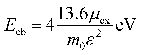 | (3) |
The optical absorption coefficients are obtained from dielectric function, as the followed equation represented:
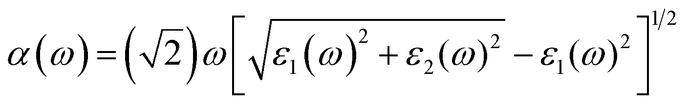 | (4) |
| ε(ω) = ε1(ω) + iε2(ω) | (5) |
Results and discussion
In recent years, the 2D inorganic perovskites Cs2PbX4 (X = Cl, Br, I) and monolayers MSe2 (M = Mo, W) have been successfully synthesized, which attracted much attention due to its highly stable structures.7,27,28 The unit cell of Cs2PbX4 perovskites belongs to cubic system and the optimized lattice parameters of monolayer Cs2PbCl4, Cs2PbBr4, Cs2PbI4 is 5.64 Å, 5.91 Å and 6.30 Å, respectively.29 [CsI]0 interface exhibits more strongly charge transferring than [PbI2]0.30 Therefore the [CsI]0 plane of the monolayer Cs2PbX4 is used to form the heterojunctions. The optimized lattice parameters of monolayer MoSe2, WSe2 are 3.32 Å.31–33 To minimize the lattice mismatch between the stacking blocks, the supercell of new Cs2PbX4–MSe2 heterostructures are built by 3 × 1 cubic phases Cs2PbCl4 and MSe2,
MSe2,  cubic phases Cs2PbBr4 and
  MSe2, and
  cubic phases Cs2PbI4 and
  MSe2, respectively, as seen in Fig. 1 (Table 1).
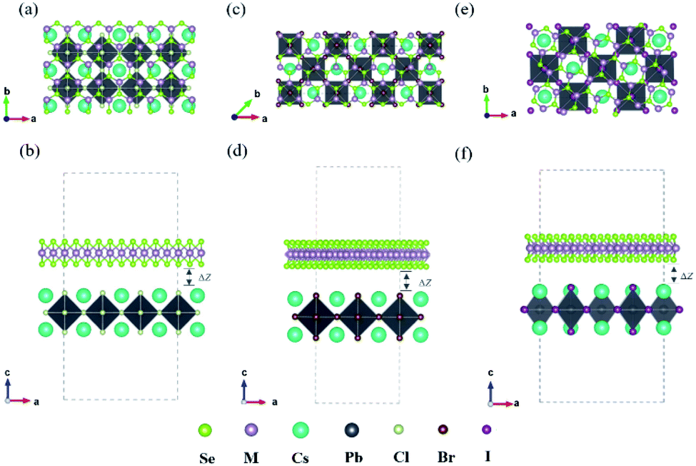 | ||
| Fig. 1 Top and side views of relaxed Cs2PbX4–MSe2 (M = Mo, W) heterostructures. (a and b) Cs2PbCl4–MSe2 heterostructure. (c and d) Cs2PbBr4–MSe2 heterostructure. (e and f) Cs2PbI4–MSe2 heterostructure. | ||
| Heterostructures | a (Å) | b (Å) | a1 (Å) | b1 (Å) | Mismatch (%) | ΔZ (Å) | Eb (meV Å−2) |
|---|---|---|---|---|---|---|---|
| Cs2PbCl4–MoSe2 | 16.51 | 5.66 | 16.75 | 5.69 | 1.10% | 3.09 | −16.73 |
| Cs2PbBr4–MoSe2 | 16.35 | 11.81 | 16.65 | 11.89 | 0.62% | 3.12 | −16.28 |
| Cs2PbBr4–MoSe2 | 18.22 | 8.66 | 18.14 | 8.84 | 1.79% | 3.16 | −16.12 |
| Cs2PbBr4–WSe2 | 16.41 | 5.67 | 16.75 | 5.69 | 1.02% | 2.90 | −17.09 |
| Cs2PbBr4–WSe2 | 16.35 | 11.81 | 16.65 | 11.89 | 0.65% | 3.18 | −17.52 |
| Cs2PbBr4–WSe2 | 18.21 | 8.66 | 18.20 | 8.67 | 1.82% | 3.30 | −15.56 |
The lattice mismatches of Cs2PbCl4–MoSe2, Cs2PbBr4–MoSe2, Cs2PbI4–MoSe2, Cs2PbCl4–WSe2, Cs2PbBr4–WSe2 and Cs2PbI4–WSe2 heterostructures are less than 1.10%, 0.62%, 1.79%, 1.02%, 0.65% and 1.82%. The optimized vertical interlayer distances of Cs2PbCl4–MoSe2, Cs2PbBr4–MoSe2, Cs2PbI4–MoSe2, Cs2PbCl4–WSe2, Cs2PbBr4–WSe2 and Cs2PbI4–WSe2 interfaces are 3.07, 3.12, 3.16, 2.90, 3.18 and 3.30 Å, respectively, which increase gradually with the halogen varying from Cl to I. Interface binding energy of Cs2PbCl4–MoSe2, Cs2PbBr4–MoSe2 and Cs2PbI4–MoSe2, Cs2PbCl4–WSe2, Cs2PbBr4–WSe2 and Cs2PbI4–WSe2 interfaces is −16.73, −16.28 and −16.12, −17.09, −17.52 and −15.56 meV Å−2, respectively. The small interface binding energy and the interlayer distance ranging from 2.9 Å to 3.3 Å indicate that 2D Cs2PbX4–MSe2 heterostructures are formed by vdW contact.33 These Eb values are comparable to Eb of InSe/GaSe (−18.25 meV Å−2), suggesting that Cs2PbX4–MSe2 heterostructures are stable in energy.34 ln addition, MoSe2–CsPbBr3 Mixed van der Waals nanohybrids also have been fabricated in experiments (Table 2).16
| Functional | Cs2PbCl4 | Cs2PbBr4 | Cs2PbI4 | MoSe2 | WSe2 |
|---|---|---|---|---|---|
| PBE | 2.59 | 2.18 | 1.84 | 1.45 | 1.56 |
| HSE | 3.58 | 2.91 | 2.57 | 2.10 | 2.03 |
| PBE + SOC | 1.84 | 1.46 | 1.09 | 1.37 | 1.33 |
| HSE + SOC | 2.78 | 2.14 | 1.78 | 1.89 | 1.93 |
| Experiment | 3.01 | 2.32 | 1.86 | 1.48 | 1.60 |
In order to study the band structures of Cs2PbX4–MSe2 heterostructures, the band structures of 2D perovskites Cs2PbX4, monolayer WSe2 and monolayer MoSe2 were calculated by different functionals, including PBE, PBE with SOC (PBE + SOC), HSE, and HSE with SOC (HSE + SOC) functionals. Monolayer MoSe2 and monolayer WSe2 show a direct band gap of 1.45 eV and 1.56 eV using PBE functional. Monolayer Cs2PbCl4, Cs2PbBr4 and Cs2PbI4 possess a direct bandgap of 2.59 eV, 2.18 eV and 1.84 eV using PBE functional. We find that the bandgaps of Cs2PbX4 computed via PBE and HSE + SOC functionals are in good agreements with experiments and other theoretical results.9,10,27,28,35–38 The band gap calculated by HSE is larger than PBE and the band gap calculated by PBE + SOC is smaller than PBE. In addition, the band gap of MSe2 calculated by HSE + SOC is larger than the related experimental data.27,28 This is because the HSE functional usually overcorrects slightly the band gap of an intrinsic semiconductor.39 Thus, in order to accurately and closely study the contact characteristics of Cs2PbX4–MSe2 heterostructures, PBE is employed in the following heterostructures section. When monolayers Cs2PbX4 and MSe2 (M = Mo, W) are contacted to make up Cs2PbX4–MSe2 heterostructures, the electronic structures of Cs2PbX4–MSe2 heterostructures are shown in Fig. 2. The Cs2PbCl4–MoSe2, Cs2PbBr4–MoSe2, Cs2PbI4–MoSe2, Cs2PbCl4–WSe2, Cs2PbBr4–WSe2 and Cs2PbI4–WSe2 heterostructures have an indirect bandgap with the value of 1.30 eV, 1.48 eV, 1.54 eV, 1.33 eV, 1.67 eV and 1.53 eV, which approach optimal bandgap (1.34 eV) for solar cells.40 Moreover, the conduction band minimum (CBM) of Cs2PbX4–MSe2 heterostructures are dominated by the MSe2 layer and the valence band maximum (VBM) of Cs2PbX4–MSe2 heterostructures are dominated by Cs2PbX4 part.
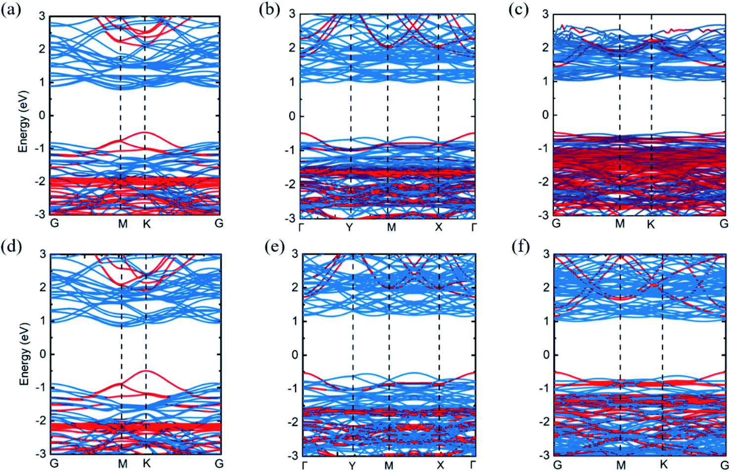 | ||
| Fig. 2 Band structures of Cs2PbX4–MSe2 heterostructures (a) X = Cl, M = Mo; (b) X = Br, M = Mo; (c) X = I, M = Mo; (d) X = Cl, M = W; (e) X = Br, M = W; (f) X = I, M = W. The red and blue lines correspond to Cs2PbX4 and MSe2, respectively. | ||
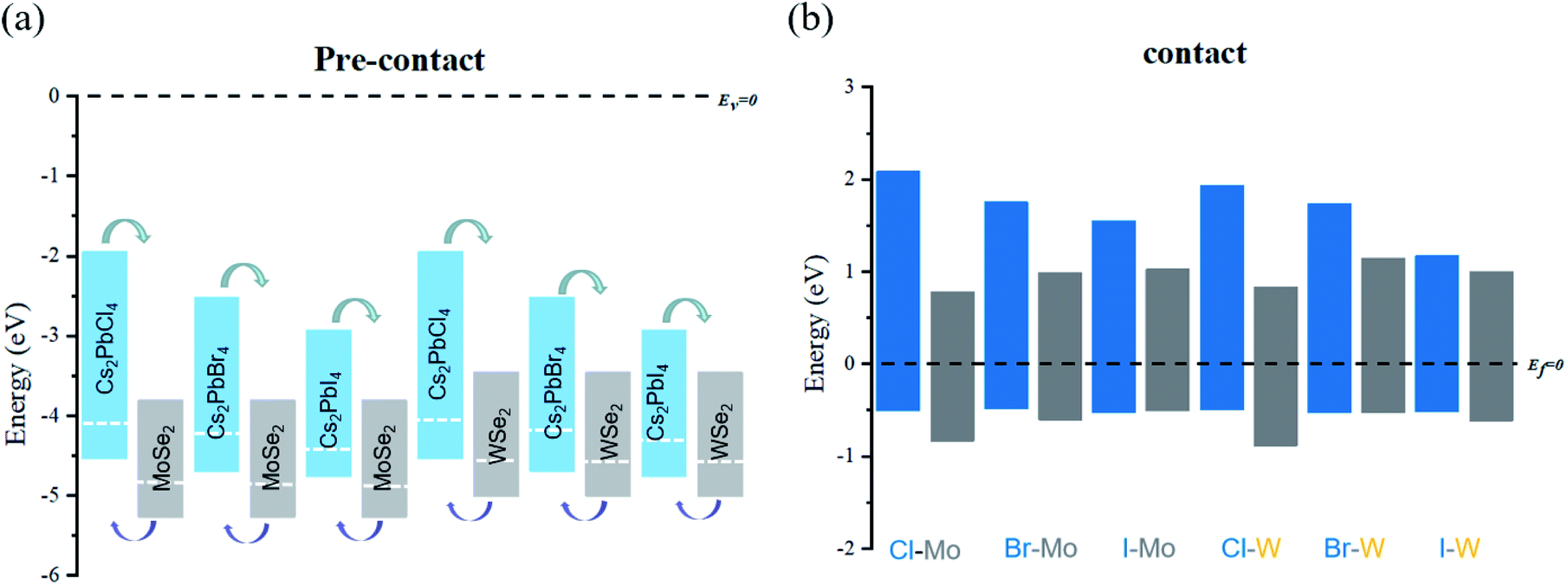
The analysis of energy level arrangement is of great significance to further study interface properties of Cs2PbX4–MSe2 heterostructures. The vacuum energy level (Ev) is set to zero in the precontact state and the Fermi level (Ef) is set to zero in the contact state. In precontact state, the CBM and VBM of monolayer Cs2PbX4 are both higher than that of monolayer MSe2 and both Cs2PbX4–MSe2 are type-II heterostructures, as seen in Fig. 3(a). The electrons will diffuse from monolayers Cs2PbX4 to monolayers MSe2 and the holes will move from monolayers MSe2 monolayer to monolayers s2PbX4 when they contact. Correspondingly, the holes accumulate in Cs2PbX4 monolayers and the electrons accumulate in MSe2 monolayers. Moreover, the difference between the vacuum level and the Fermi level is defined as the work function.31 The work function is the internal dynamics of electron flow. The computed work functions of monolayers Cs2PbCl4, Cs2PbBr4, Cs2PbI4, MoSe2 and WSe2 are 4.08 eV, 4.21 eV, 4.30 eV, 4.83 eV and 4.51 eV, respectively. The heterostructures are mainly related to the work function after contact. In order to maintain Fermi levels at the same level after contact, the Fermi level of all Cs2PbX4 perovskites moved down and the Fermi level of monolayer MSe2 moved up after they contact each other.
 | ||
| Fig. 3 Energy level graphs of the monolayer MSe2 and Cs2PbX4 in the precontact (a) and contact (b). Blue and gray rectangles represent the monolayer Cs2PbX4 and MSe2. The bottom and top of rectangles correspond to VBM and CBM, respectively. | ||
The energy level diagram of Cs2PbX4–MSe2 heterostructures in contact states is given in Fig. 3(b). The Cs2PbX4–MSe2 heterostructures are type-II heterostructures, which can drive the photogenerated holes and electrons to move in opposite directions, resulting in spatial separation of holes and electrons on different sides of heterostructures.33 Thus, Cs2PbX4–MSe2 heterostructures are beneficial for improving the photoelectric conversion efficiency of Cs2PbX4–MSe2 optoelectronic applications. In these type-II heterostructures, the differences between the VBM of their components (valence band offset, Δv) are crucial for hole blocking and the differences between the CBM of their components (conduction band offset, Δc) are crucial for electron transport. The large Δv promotes hole extraction from TMDs layers to perovskite layers and the large Δc allows free electrons to move from perovskite to TMDs layers. It is shown that Cs2PbCl4–MSe2 heterostructure have the largest Δc and Δv among Cs2PbX4–MSe2 heterostructures.12 Thus, the Cs2PbCl4–MoSe2, and Cs2PbCl4–WSe2 heterostructures may have the largest charge transport power and are more conducive to reducing the dark current. In addition, Cs2PbX4–MoSe2 heterostructures have lager Δc and Δv than Cs2PbX4–WSe2 heterostructures.
In addition, the Mott–Wananier theory has been used to approximate exciton binding energies in the vdW heterostructures.41 Table 3 lists the carrier masses and MW exciton binding energy of Cs2PbX4–MSe2 heterostructures. The lower exciton binding energies usually facilitate the splitting of excitons into free charge carriers.34 It is shown that Cs2PbCl4–MoSe2 heterostructures exhibit the lowest exciton binding energies among Cs2PbX4–MoSe2 heterostructures. Therefore, Cs2PbCl4–MoSe2 heterostructures can effectively promotes the separation of excitons and exhibit the highest charge transport efficiency among Cs2PbX4–MSe2 heterostructures.
| Heterostructures | me (m0) | mh (m0) | μex (m0) | ε | Eeb (eV) |
|---|---|---|---|---|---|
| Cs2PbCl4–MoSe2 | 1.16 | 0.28 | 0.23 | 5.34 | 0.43 |
| Cs2PbBr4–MoSe2 | 0.79 | 0.71 | 0.37 | 5.44 | 0.68 |
| Cs2PbI4–MoSe2 | 1.39 | 0.67 | 0.45 | 5.24 | 1.00 |
| Cs2PbCl4–WSe2 | 1.46 | 0.27 | 0.23 | 4.95 | 0.50 |
| Cs2PbBr4–WSe2 | 0.75 | 0.66 | 0.35 | 5.08 | 0.74 |
| Cs2PbI4–WSe2 | 1.03 | 0.61 | 0.38 | 5.26 | 0.76 |
To clearly investigate the recombination rates of electron–hole pairs and transfer of charges between the Cs2PbX4 monolayers and MSe2 monolayers across the interfaces, the plane-averaged charge density difference Δρ are calculated, as shown in Fig. 4. The results demonstrate that the holes mainly accumulated at the Cs2PbX4 interfaces and the charges accumulated at MSe2 interfaces. Additionally, the charges transfer from Cs2PbX4 interfaces to MSe2 interfaces while the holes move in the opposite direction. The direction of charge transfer is consistent with that of band alignment analysis, which shown type-II heterostructures are benefited to the separation of electrons and holes. What's more, detail charge transfers among interlayer spacing are used to quantitatively evaluate charge transferring of heterostructures. The Cs2PbCl4–MoSe2, Cs2PbBr4–MoSe2, Cs2PbI4–MoSe2, Cs2PbCl4–WSe2, Cs2PbBr4–WSe2 and Cs2PbI4–WSe2 heterostructures have charge transfers among interlayer spacing with the values of 0.18, 0.15, 0.16, 0.16, 0.10 and 0.14 × 10⁻³e. We find that the Cs2PbCl4–MSe2 heterostructures have the highest charge transfers in the six Cs2PbX4–MSe2 heterostructures among interlayer spacing. In addition, Cs2PbX4–MoSe2 heterostructures have larger charge transfers than Cs2PbX4–WSe2 heterostructures. It is because Cs2PbX4–MoSe2 heterostructures have smaller exciton binding energies than Cs2PbX4–WSe2 heterostructures.
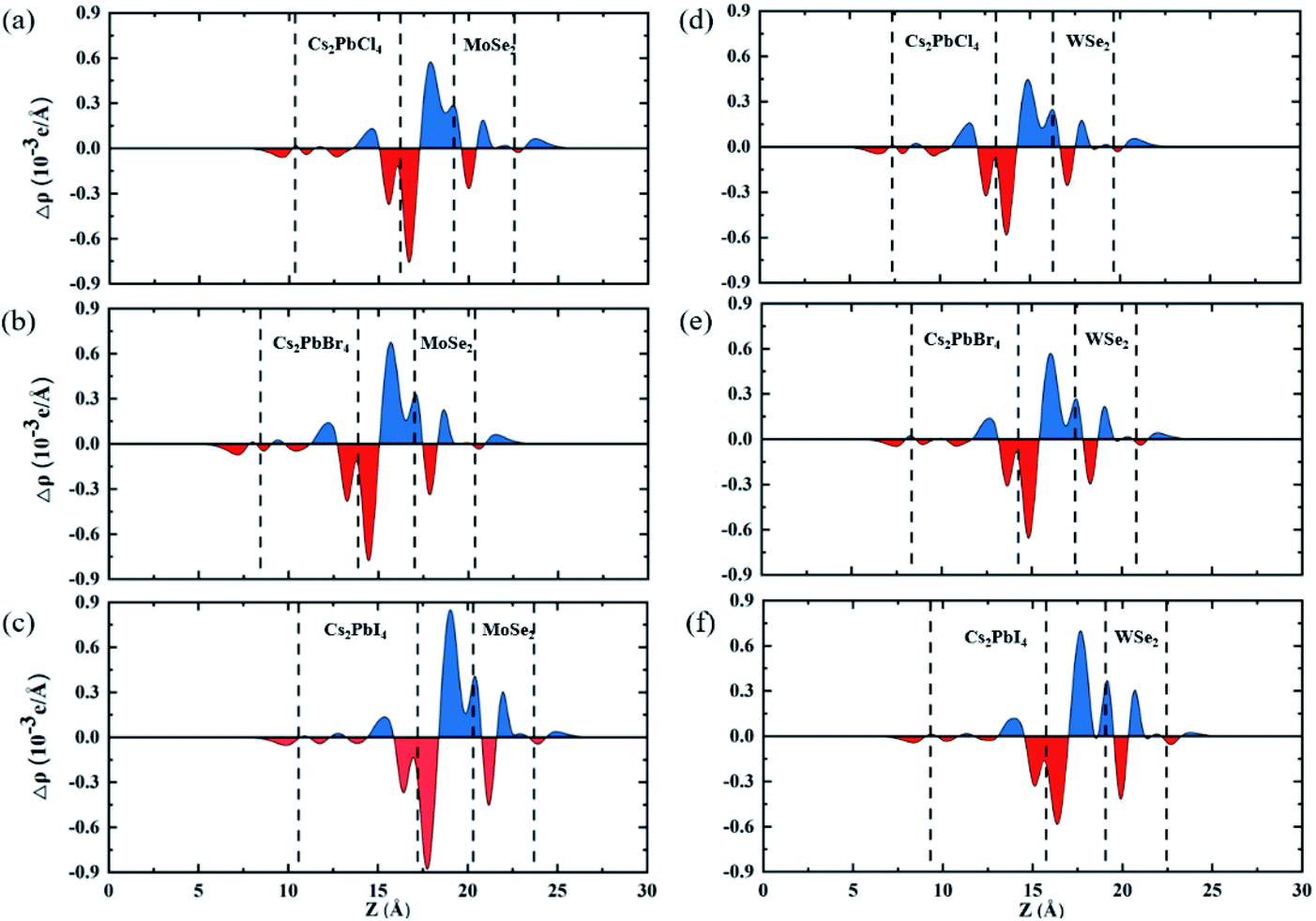 | ||
| Fig. 4 The planar-averaged differential charge density Δρ(z) of Cs2PbX4–MSe2 heterostructures: (a and d) X = Cl; (b and e) X = Br; (c and f) X = I. Red and blue represent electron depletion and accumulation. | ||
Except for the electronic structures and charge redistributions of heterostructures, the optical properties in vdW heterostructures have important effects on the performance of perovskite optoelectronic devices.42 In order to further study the optical properties of Cs2PbX4–MSe2 heterostructures, the optical absorption coefficients were calculated, as shown in Fig. 5. The optical absorption coefficients of MSe2 monolayers are higher than those of Cs2PbX4 monolayers. The optical absorption coefficients of all heterostructures are significantly higher than those of corresponding Cs2PbX4 monolayers and MSe2 monolayers. This is because the bandgaps of 2D Cs2PbX4–MSe2 heterostructures are smaller than the bandgaps of Cs2PbX4 monolayers. The bandgaps of Cs2PbX4–MSe2 heterostructures approach optimal bandgap (1.34 eV) for solar cells.40 Thus, the construction of Cs2PbX4–MSe2 heterostructures is beneficial to improve the light absorption of optoelectronic devices.
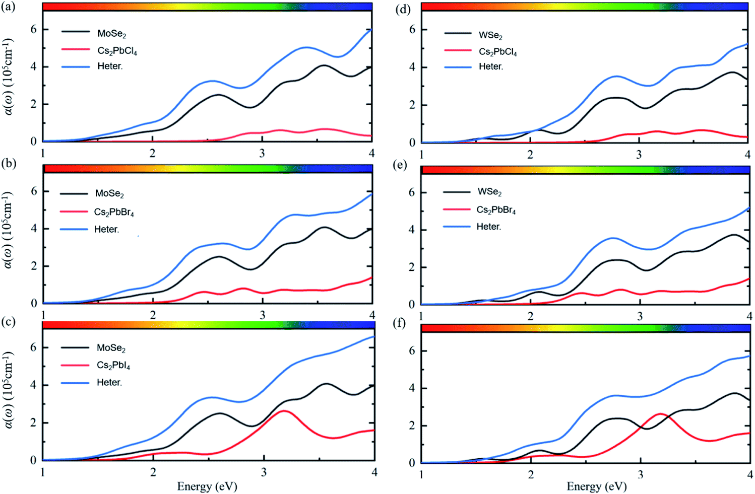 | ||
| Fig. 5 Optical absorption coefficients of (a and d) Cs2PbCl4–MSe2, (b and e) Cs2PbBr4–MSe2, and (c and f) Cs2PbI4–MSe2 heterostructures. The blue, black and red lines represent optical absorption spectrum of heterostructures, monolayer MSe2 and Cs2PbX4, respectively. | ||
In addition, the light absorption of Cs2PbX4–MoSe2 heterostructures is only slightly greater than that of Cs2PbX4–WSe2 in the visible region because the light absorption of MoSe2 is slightly greater than that of WSe2 in the visible region. The light absorption coefficients of Cs2PbX4 increase rapidly in the visible region with the halogen varying from Cl to I. The light absorption coefficients of Cs2PbX4–MSe2 heterostructures increase rapidly in the visible region with the halogen varying from Cl to I. Therefore, the Cs2PbI4–MSe2 heterostructure has great potential application in solar cells among Cs2PbX4–MSe2 heterostructures.
In order to explore the application of Cs2PbX4–MSe2 heterostructures in solar cells, we further calculated the power conversion efficiency of Cs2PbX4–MSe2 heterostructures. The PCE depends on the donor band gap and conduction band offset.43,44 The PCE of Cs2PbX4–MSe2 heterostructures with type-II alignment is shown in Fig. 6 as a contour plot where the x- and y-axes are the donor band gap and conduction band offset, respectively. The PCE of Cs2PbI4–MoSe2, Cs2PbI4–WSe2 and Cs2PbBr4–WSe2 heterostructures is 13%, 18% and 10%, which is greater than 10%. Three heterostructures can be used in solar cells. Cs2PbI4–WSe2 heterostructure has the largest PCE (18%) among Cs2PbX4–MSe2 heterostructures. The PCE of Cs2PbI4–WSe2 heterostructure is larger than that of WS2/CsPbBr3 PSCs (10.65%) and WSe2–mediated PSCs (16.3%).13,18 With the halogen varying from Cl to I, the PCE of Cs2PbX4–WSe2 heterostructures increase rapidly. The PCE variation trend is consistent with the absorption coefficients of Cs2PbX4–MSe2 heterostructures varying from Cl to I. In addition, the PCE of Cs2PbX4–WSe2 heterostructures is larger than the PCE of Cs2PbX4–MoSe2 heterostructures. This is mainly because Cs2PbX4–WSe2 heterostructures have smaller Δc than Cs2PbX4–MoSe2 heterostructures. Therefore, Cs2PbI4–WSe2 heterostructure has great potential application in solar cells.
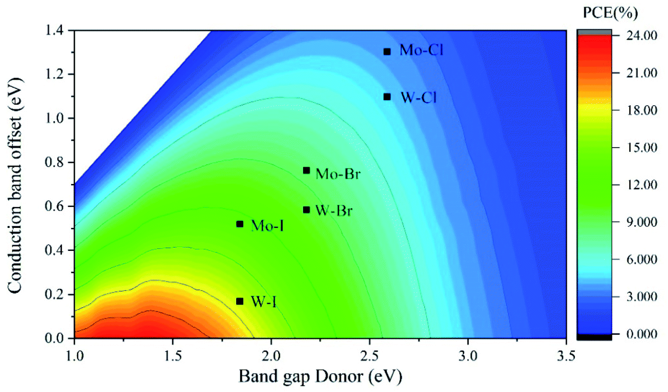 | ||
| Fig. 6 Contour plot showing the calculated PCE of Cs2PbX4–MSe2 heterostructures according to the Cs2PbX4 donor band gap and conduction band offset Δc. | ||
Conclusions
In summary, we have systematically studied the structural, stability, charge transfer and optoelectronic properties of 2D perovskite Cs2PbX4–MSe2 heterostructures with different halide elements based on density functional calculations. All these six heterostructures are stable in energy and the interlayer distances increase gradually with the halogen varying from Cl to I. Electronic structures show Cs2PbX4–MSe2 heterostructures belongs to type-II energy level shifts with narrower optical gap than monolayers Cs2PbX4. In addition, the Cs2PbCl4–MoSe2, and Cs2PbCl4–WSe2 heterostructures may have the largest charge transport power due to their larger band offset, which is beneficial to reduce dark current and improve open circuit voltage. Cs2PbCl4–MoSe2 heterostructures can effectively promotes the separation of excitons and exhibit the highest charge transport efficiency among Cs2PbX4–MSe2 heterostructures due to their lowest exciton binding energies. Cs2PbCl4–MoSe2 heterostructure has the potential to be applied in photodetectors. Next, the charges transfer from Cs2PbX4 interfaces to MSe2 interfaces while the holes move in the opposite direction. The holes mainly accumulated at the Cs2PbX4 interfaces and the charges accumulated at MSe2 interfaces. Cs2PbX4–MoSe2 heterostructures have larger charge transfers than Cs2PbX4–WSe2 heterostructures. Finally, optical absorptions of six heterostructures are significantly higher than the corresponding Cs2PbX4 monolayers and MSe2 monolayers. The PCE of Cs2PbX4–WSe2 heterostructures is larger than the PCE of Cs2PbX4–MoSe2 heterostructures. Cs2PbI4–WSe2 heterostructure has the largest PCE (18%) among Cs2PbX4–MSe2 heterostructures. In conclusion, Cs2PbCl4–MoSe2 heterostructure exhibits great potential application in photodetectors devices and Cs2PbI4–WSe2 heterostructure has great potential application in solar cells. Our findings provide insight into of Cs2PbX4–MSe2 heterostructures can effectively improve the performance of perovskite optoelectronic devices.Conflicts of interest
There are no conflicts to declare.Acknowledgements
This work is supported by the Fund of State Key Laboratory of IPOC(BUPT) (no. IPOC2019ZZ04) and the Open-Foundation of Key Laboratory of Laser Device Technology, China North Industries Group Corporation Limited (Grant No. KLLDT202103). We thank for the helpful discussion with Prof. Pengfei Guan and the computational support from the Beijing Computational Science Research Center (CSRC). We also acknowledge the computation supported by High-performance Computing Platform of BUPT.Notes and references
- A. T. Barrows, A. J. Pearson, C. K. Kwak, A. D. F. Dunbar, A. R. Buckley and D. G. Lidzey, Energy Environ. Sci., 2014, 7, 2944–2950 RSC.
- K. Xiao, R. Lin, Q. Han, Y. Hou, Z. Qin, H. T. Nguyen, J. Wen, M. Wei, V. Yeddu, M. I. Saidaminov, Y. Gao, X. Luo, Y. Wang, H. Gao, C. Zhang, J. Xu, J. Zhu, E. H. Sargent and H. Tan, Nat. Energy, 2020, 5, 870–880 CrossRef CAS.
- I. L. Braly, D. W. deQilettes, L. M. Pazos-Outon, S. Burke, M. E. Ziffer, D. S. Ginger and H. W. Hillhouse, Nat. Photonics, 2018, 12, 355–361 CrossRef CAS.
- M. M. Lee, J. Teuscher, T. Miyasaka, T. N. Murakami and H. J. Snaith, Science, 2012, 338, 643–647 CrossRef CAS PubMed.
- J. H. Noh, S. H. Im, J. H. Heo, T. N. Mandal and S. I. Seok, Nano Lett., 2013, 13, 1764–1769 CrossRef CAS PubMed.
- Y.-Y. Zhang, S. Chen, P. Xu, H. Xiang, X.-G. Gong, A. Walsh and S.-H. Wei, Chin. Phys. Lett., 2018, 35, 036104 CrossRef.
- S. Chen and G. Shi, Adv. Mater., 2017, 29, 1605448 CrossRef PubMed.
- Y. F. Ding, Q. Q. Zhao, Z. L. Yu, Y. Q. Zhao, B. Liu, P. B. He, H. Zhou, K. L. Li, S. F. Yin and M. Q. Cai, J. Mater. Chem. C, 2019, 7, 7433–7441 RSC.
- A. Bala, A. K. Deb and V. Kumar, J. Phys. Chem. C, 2018, 122, 7464–7473 CrossRef CAS.
- J. Song, L. Xu, J. Li, J. Xue, Y. Dong, X. Li and H. Zeng, Adv. Mater., 2016, 28, 4861–4869 CrossRef CAS PubMed.
- E. Shi, Y. Gao, B. P. Finkenauer, A. Akriti, A. H. Coffey and L. Dou, Chem. Soc. Rev., 2018, 47, 6046–6072 RSC.
- J. He, J. Su, Z. Lin, S. Zhang, Y. Qin, J. Zhang, J. Chang and Y. Hao, J. Phys. Chem. C, 2019, 123, 7158–7165 CrossRef CAS.
- Q. W. Zhou, J. L. Duan, X. Y. Yang, Y. Y. Duan and Q. W. Tang, Angew. Chem., Int. Ed., 2020, 132, 22181–22185 CrossRef.
- J. P. Cao, G. Q. Tang, P. You, T. Y. Wang, F. Y. Zheng, J. Zhao and F. Yan, Adv. Funct. Mater., 2020, 30, 2002358 CrossRef CAS.
- Hybrid Bilayer WSe2-CH3NH3PbI3 Organolead Halide Perovskite as a High-Performance Photodetector.
- S. Hassan, P. Basera, S. Bera, M. Mittal, S. K. Ray, S. Bhattacharya and S. Sapra, ACS Appl. Mater. Interfaces, 2020, 12, 7217–7325 Search PubMed.
- S.-H. Lee, J. Y. Kim, S. Choi, Y. Lee, K.-S. Lee, J. Kim and J. Joo, ACS Appl. Mater. Interfaces, 2020, 12, 25159–25167 CrossRef CAS PubMed.
- Y. Choi, S. Jung, N. K. Oh, J. Lee, J. Seo, U. Kim, D. Koo and H. Park, Enhanced charge transport via metallic 1T phase transition metal dichalcogenides-mediated hole transport layer engineering for perovskite solar cells, Chemnanomat, 2019, 5, 1050–1058 CrossRef CAS.
- G. Kresse and D. Joubert, Phys. Rev. B: Condens. Matter Mater. Phys., 1999, 59, 1758–1775 CrossRef CAS.
- J. P. Perdew, K. Burke and M. Ernzerhof, Phys. Rev. Lett., 1996, 77, 3865–3868 CrossRef CAS PubMed.
- P. E. Blochl, Phys. Rev. B: Condens. Matter Mater. Phys., 1994, 50, 17953–17979 CrossRef PubMed.
- B. Jia, P. Zhu, S. Sun, L. Han, G. Liu, Y. Wang, G.-D. Peng and P. Lu, IEEE J. Sel. Top. Quantum Electron., 2019, 26, 1–6 Search PubMed.
- S. Lin, J. C. Liu, W. Z. Li, D. Wang, Y. Huang, C. Jia, Z. W. Li, H. Y. Wang, J. N. Song, Z. L. Liu, K. Huang, D. Zu, M. Lei, B. Hong and H. Wu, Nano Lett., 2019, 19, 6853–6861 CrossRef CAS PubMed.
- J. C. Xu, K. Bi, R. Zhang, Y. N. Hao, C. W. Lan, M.-M. Klaus, X. J. Zhai, Z. D. Zhang and S. G. H, Research, 2019, 2019, 9686213 Search PubMed.
- X. N. Guan, R. Zhang, B. N. Jia, L. Y. Wu, B. Zhou, L. Fan, G. Liu, Y. Wang, P. F. Lu and G. D. Peng, J. Non-Cryst. Solids, 2020, 550, 120388 CrossRef CAS.
- P. F. Lu, J. Sichuan Norm. Univ., Nat. Sci., 2020, 43, 1–20 Search PubMed.
- X. Wang, Y. Gong, G. Shi, W. L. Chow, K. Keyshar, G. Ye, R. Vajtai, J. Lou, Z. Liu, E. Ringe, B. K. Tay and P. M. Ajayan, ACS Nano, 2014, 8, 5125–5131 CrossRef CAS PubMed.
- J.-K. Huang, J. Pu, C.-L. Hsu, M.-H. Chiu, Z.-Y. Juang, Y.-H. Chang, W.-H. Chang, Y. Iwasa, T. Takenobu and L.-J. Li, ACS Nano, 2014, 8(1), 923–930 CrossRef CAS PubMed.
- J.-H. Yang, Q. Yuan and B. I. Yakobson, J. Phys. Chem. C, 2016, 120, 24682–24687 CrossRef CAS.
- Y.-Q. Zhao, Y. Xu, D.-F. Zou, J.-N. Wang, G.-F. Xie, B. Liu, M.-Q. Cai and S.-L. Jiang, J. Phys.: Condens. Matter, 2020, 32, 195501 CrossRef CAS PubMed.
- Y. Ding, Y. Wang, J. Ni, L. Shi, S. Shi and W. Tang, Phys. Chem. Chem. Phys., 2011, 13, 15546–15553 RSC.
- Y. Zhang, Y. Zhao, Y. Xu and L. He, Solid State Commun., 2021, 327, 114233 CrossRef CAS.
- B. Liu, M. Long, M.-Q. Cai and J. Yang, J. Phys. Chem. Lett., 2018, 327, 114233 Search PubMed.
- J. H. Chen, X. J. He, B. S. Sa, J. Zhou, C. Xu, C. L. Wen and Z. M. Sun, Nanoscale, 2019, 11, 6431–6444 RSC.
- P. Zhu, H. Zhao, X. Li, Y. Zu, L. Wu, C. Chen and G. Liu, Phys. E, 2021, 134, 114908 CrossRef CAS.
- A. Molina-Sanchez, ACS Appl. Energy Mater., 2018, 1, 6361–6367 CrossRef.
- Z. Zheng, X. X. Wang, Y. W. Shen, Z. Y. Luo, L. G. Li, L. Gan, Y. Ma, H. Q. Li, A. L. Pan and T. Y. Zhai, Adv. Opt. Mater., 2018, 6, 1800879 CrossRef.
- P. B. Gui, H. Zhou, F. Yao, Z. H. Song, B. R. Li and G. J. Fang, Small, 2019, 15, 1902618 CrossRef PubMed.
- R. J. Sutton, M. R. Filip, A. A. Haghighirad, N. Sakai, B. Wenger, F. Giustino and H. J. Snaith, ACS Energy Lett., 2018, 3, 1787–1794 CrossRef CAS.
- S. Ruhle, Sol. Energy, 2016, 130, 139–147 CrossRef.
- P. Wang, Y. X. Zong, H. Liu, H. Y. Wen, H. X. Deng, Z. M. Wei, H. B. Wu and J. B. Xia, J. Phys. Chem. C, 2020, 214, 23832–23838 CrossRef.
- W. J. Yin, J. H. Yang, J. Kang, Y. Yan and S. H. Wei, J. Mater. Chem. A, 2015, 3, 8926–8942 RSC.
- M. C. Scharber, D. Wuhlbacher, M. Koppe, P. Denk, C. Waldauf, A. J. Heeger and C. L. Brabec, Adv. Mater., 2006, 18, 189 CrossRef.
- M. Bernardi, M. Palummo and J. C. Grossman, ACS Nano, 2012, 6, 10082–10089 CrossRef CAS PubMed.
| This journal is © The Royal Society of Chemistry 2022 |