
 Open Access Article
 This Open Access Article is licensed under a Creative Commons Attribution-Non Commercial 3.0 Unported Licence
Pen-writing high-quality perovskite films and degradable optoelectronic devices†
Ting Zhanga,
Shasha Zhanga,
Zhenkun Gu*a,
Rudai Zhaoa,
Shiheng Wanga,
Lutong Guobc,
Tiesheng Li a,
Yiqiang Zhanga and
Yanlin Song*bc
a,
Yiqiang Zhanga and
Yanlin Song*bc
aGreen Catalysis Center, College of Chemistry, Henan Institute of Advanced Technology, Zhengzhou University, Zhengzhou 450051, China. E-mail: guzhenkun@zzu.edu.cn
bKey Laboratory of Green Printing, Institute of Chemistry, Chinese Academy of Sciences, Beijing 100190, China. E-mail: ylsong@iccas.ac.cn
cUniversity of Chinese Academy of Sciences, Beijing 100049, China
First published on 31st January 2022
Abstract
Paper is ubiquitous in the daily life and has been widely used for writing and drawing because of their low-cost, widely accessible, and degradable properties. However, simple ways to fabricate paper-based optoelectronic devices remain a great challenge. In this work, we report a facile method to fabricate high-quality perovskite films and optoelectronic devices on paper by direct pen-writing. Through introducing seed layers on papers, planar-integrated single-crystal perovskite films are easily prepared using commercial pens. Based on such a simple and convenient method, perovskite photodetector arrays and image sensors with graphite electrodes are fabricated on paper, and show satisfactory performances. This method provides a simple and effective approach for preparation of paper-based perovskite devices. It will be of significance for the development of degradable optoelectronic devices.
1. Introduction
Perovskites have been widely applied in solar cells,1–4 light-emitting diodes,5–7 photodetectors8–10 and lasers11 due to their facile solution-processability, long carrier diffusion length and high carrier mobility.12 Recently, flexible optoelectronic devices have attracted intensive interest because of their promising applications in wearable devices, biosensors and smart textiles. To fabricate flexible optoelectronic devices, all photosensitive materials, electrodes and substrates must be optimized to meet the requirements of flexibility, light weight, low cost and stability.13–15 To date, diverse plastic substrates, such as polyethylene terephthalate (PET) and poly(ethylene naphthalate) (PEN), are used to fabricate flexible perovskite optoelectronic devices.16–19 Li and co-workers demonstrated a solution method to fabricate photodetector on a PET substrate, which displayed a high on/off ratio and responsivity.20 Li et al. reported a flexible photodetector on ITO/PEN substrate with outstanding stability and satisfactory detectivity.21 However, low thermal durability and high thermal expansion coefficient of plastics always obstruct the manufacturing processes. More importantly, plastic substrates are difficult to degrade in nature.Paper is usually made of natural cellulose fibers, it can be degraded completely in 6 weeks.22,23 Recently, paper is considered as a promising substrate material for flexible electronics because of its lightweight, deformability, and biodegradability, which accords with the development trend of modern electronic products towards flexible devices.22,24 Chu et al. reported a dual-source physical vapor deposition processed photodetector on cellulose paper substrates with high photo detecting performance.25 Yang and coworkers prepared the flexible photodetector arrays on common paper by an all-sprayed-processable method.26 However, these traditional methods are complicated and time-consuming. More importantly, the perovskite crystals by these methods have poor quality. Therefore, the development of a facile approach to fabricate paper-based perovskite optoelectronic devices is of significance.27–29
Herein, we report a facile method to construct high-quality perovskite films and devices on paper by pen-writing. Through introducing the seed layers on paper, planar-integrated single-crystal perovskite films are prepared by commercial pens. Using perovskite material and graphite as the photosensitive layer and electrode, large-scale photodetector arrays are easily written on paper. The photodetector presents a responsivity of 4.2 mA W−1 at a low operational bias voltage of 4 V. Furthermore, an image sensor is fabricated, which shows satisfied performance. This method provides a simple and effective strategy for the development of paper-based optoelectronic devices.
2. Experimental section
2.1 Material
Methylammonium bromide (CH3NH3Br; ≥99.5%) was purchased from Xi'an Polymer Light Technology Corp. Lead bromide (PbBr2; 99.999%) and N,N-dimethylformamide (DMF, ≥99.9%) were purchased from Aladdin Reagent Ltd. The weighing paper was purchased from Wuxi Shangrui Paper Co., Ltd. The office-copy paper was purchased from Yalong Paper Products (Kunshan) Co., Ltd. The filter paper was purchased from Hangzhou Special Paper Co., Ltd. All these materials were used as received without further purification.2.2 Preparation of CH3NH3PbBr3 solution
PbBr2 and CH3NH3Br were dissolved in DMF and stirred at 60 °C for 6 h to prepare the 0.5 mol L−1 CH3NH3PbBr3 solution.2.3 Preparation of perovskite films by pen-writing
0.5 mol L−1 CH3NH3PbBr3–DMF was written on paper by a commercial pen (Geemarker, Hong Kong, China) with controlled speed and temperature.2.4 Spin-coating
Before spin-coating, the weighing paper was treated with UV-ozone for 15 min. 0.5 mol L−1 CH3NH3PbBr3–DMF was spin-coated on the paper at 1000 rpm for 30 s and then annealed at 80 °C for 5 min in ambient air. The film was cooled to room temperature, and the spin-coating was continued under the same conditions for 5 times.2.5 Device fabrication
Graphite-pencil (9B) drawing guided by ruler and masks was repeated 20 times to form a stripe of uniform electrode on office-copy paper. The left and right pencil-traces were both 2 mm wide and 50 mm long. The spacing between adjacent electrodes was about 300 μm. Filled the ink into the pen, and fixed the pen on a dispenser (Nordson) for writing. Placed the paper on a hot plate at 80 °C, and chose an appropriate speed to write on the paper. After solvent evaporation, the photodetector was obtained.2.6 Characterization
The crystals were examined by X-ray diffraction (XRD) with Cu Kα radiation (Empyrean, Holland). Optical images of perovskite single-crystal films were obtained using a Nikon LV100ND optical microscope. Scanning electron microscopy (SEM) image was measured by JEOL JSM-7500F (Japan). Transmission electron microscopy (TEM) images were characterized by JEOL JEM-1011 (Japan). The absorption was performed by ultraviolet-visible (UV-vis) spectrophotometer (Shimadzu UV 2600). The photoluminescence (PL) was measured with the wavelength ranging from 510 to 650 nm at room temperature by a fluorescence spectrophotometer (Horbia FluoroMax+). Time-resolved photoluminescence (TRPL) spectrum was tested using an Edinburgh Instruments FS980 system. The current–voltage (I–V) traces were measured using a Micromanipulator probe station with a Keithley 4200 semiconductor measurement system at room temperature.3. Results and discussion
Fig. 1a shows the schematic illustration of the preparation of perovskite films by pen-writing. First, perovskite solution was written on paper to form a perovskite seed layer. Then, perovskite ink was written on the seed layer for several times, and a planar-integrated single-crystal perovskite film was obtained. The morphology of pen-writing perovskite films is shown in Fig. 1b and c. It reveals that the paper substrate is covered with a dense perovskite film. In the film, the crystals are connected to each other well, forming a laterally continuous planar-integrated single-crystal perovskite structure.30,31 To further confirm the high structural order of the planar-integrated single-crystal perovskite films, transmission electron microscopy (TEM) was performed (Fig. 1d). The well-defined Bragg reflection in symmetric TEM pattern confirms the single crystal structure of the integrated crystals.32 Fig. 1g presents the X-ray diffraction (XRD) of the CH3NH3PbBr3 film. It shows a set of diffraction peaks at 14.83°, 20.92°, 29.92°, 33.57°, 37.06°, 42.98°, 45.75° and 48.34°, corresponding to the (100), (110), (200), (210), (211), (220), (300) and (310) planes of the CH3NH3PbBr3 crystal, respectively.33 The sharp diffraction peaks demonstrate the perovskite structure with high purity. | ||
| Fig. 1 (a) Schematic illustration of pen-writing perovskite films. (b and c) SEM images of the pen-writing CH3NH3PbBr3 films. (d) TEM of individual grain of CH3NH3PbBr3 films. (e) Visible absorption and PL spectra of the prepared CH3NH3PbBr3 films. (f) PL time decay trace of the CH3NH3PbBr3 films. (g) XRD data of the CH3NH3PbBr3 films. | ||
To investigate the quality of the perovskite film, the visible absorption and photoluminescence (PL) spectra were characterized. The absorption profile shows that the band edge is located at 571 nm, while the PL peak position of CH3NH3PbBr3 film is located at 560 nm (Fig. 1e). This low Stokes shift indicates a small vibronic relaxation.30 Compared with the spin-coated film (Fig. S1†), the steep rise at the band edge in the absorption spectrum suggests a low concentration of in-gap defects.30,34 The PL emission peak presents a red shift, which is closer to the PL emission peak of the bulk crystal, indicating that the films prepared by this method have a high crystal quality.35,36 Moreover, the narrow full width at half maximum (FWHM) of the PL spectrum also indicates that the film has low defects. PL decay has been widely used as a figure of merit for carrier recombination. It shows a fast and a slow time constant of τ1 ∼ 29.02 ns and τ2 ∼ 186.5 ns (Fig. 1f), which are associated with surface and bulk recombination, respectively. The charge carrier lifetimes of the pen-writing perovskite film (τ1 ∼ 29.02 ns and τ2 ∼ 186.5 ns) are much longer than the spin-coated film ( ∼ 3.7 ns and
  ∼ 14.83 ns), indicating a lower trap density of the pen-writing film (Fig. S2†).
The scanning electron microscopy (SEM) images of CH3NH3PbBr3 films of different writing times are shown in Fig. 2a–d. When the writing times are less than 5, there is less crystal on the paper and the crystal size is small, with an average size below 10 μm (Fig. 2a and b). With the increase of writing cycles, the crystal size and crystal coverage are gradually increasing. When the writing times are 10, the crystals almost completely cover the paper, while there are still a few holes on the surface (Fig. 2c). With the increase of writing times, the crystal size increases obviously and the film surface becomes denser (Fig. 2d). Finally, an integrated single-crystal perovskite film was prepared.
 | ||
| Fig. 2 (a–d) SEM images of the CH3NH3PbBr3 films prepared on paper with different writing cycles. (a) 1 times, (b) 5 times, (c) 10 times, (d) 15 times. (e) The sizes of crystals as a function of writing times. (f) The coverage of films as a function of writing times. | ||
It suggests that the writing times have a great influence on the formation of integrated single-crystal perovskite films. We investigated the crystallization process of the pen-writing perovskite films (Fig. S3†). It showed that when the writing finished for the first time, the evaporation of solvent has not been completed due to the fast-writing speed (Movie S1†). After the evaporation of solvent, a perovskite seed layer was formed because of the low nucleation barrier caused by the roughness of paper surface. With the writing times increase, fresh perovskite solution is continuously supplied. It was found that the seed crystals were in situ grown, eventually forming an integrated single-crystal perovskite film.
Based on this mechanism, planar-integrated single-crystal perovskite films can be effectively prepared on different kinds of paper, including filter paper, office-copy paper and weighing paper (Fig. 3). The corresponding SEM images show that all the papers can form satisfied perovskite films by pen-writing. It provides a promising way to construct paper-based perovskite devices.
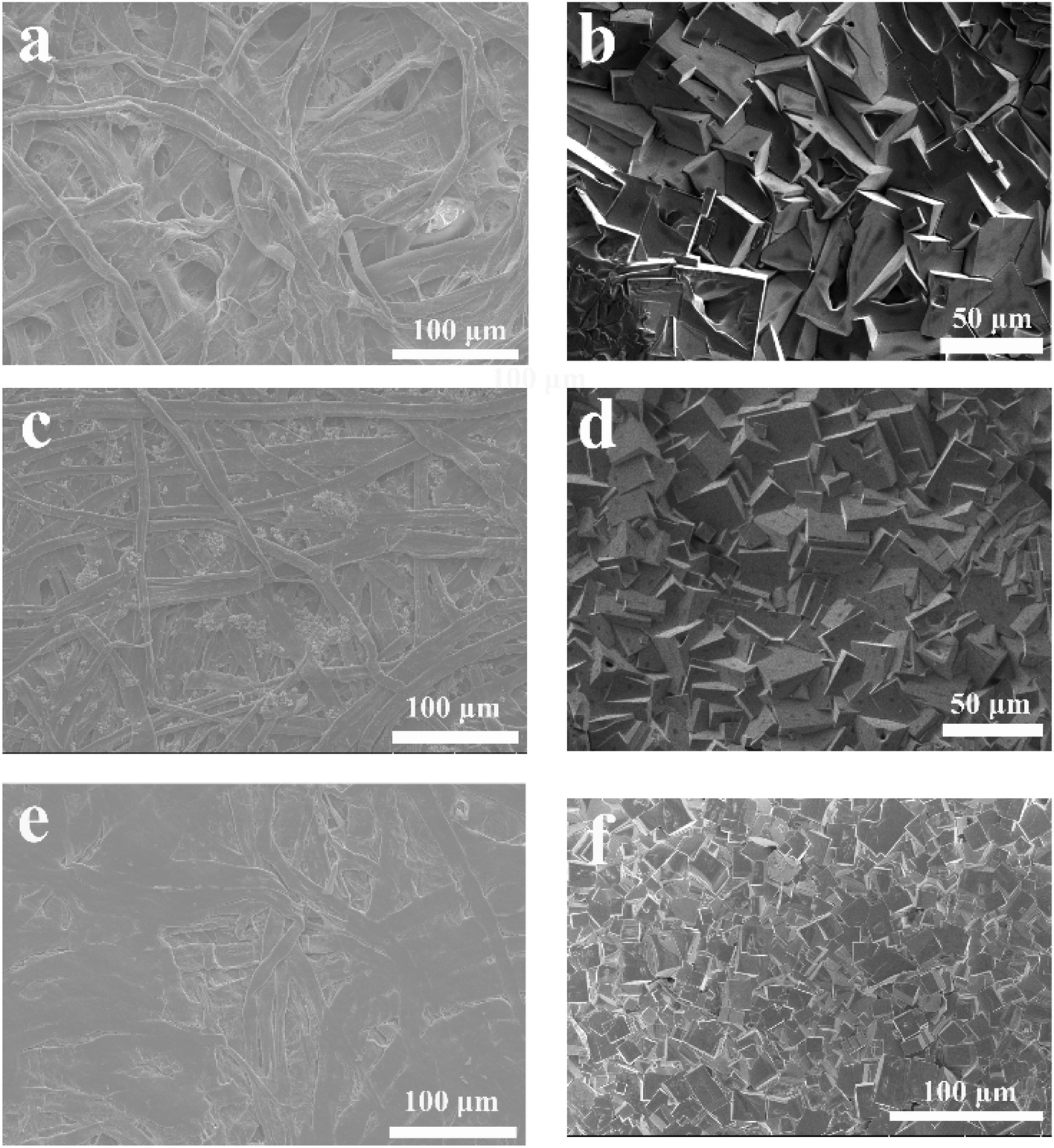 | ||
| Fig. 3 SEM of the bare paper and CH3NH3PbBr3 films. (a) Filter paper. (b) CH3NH3PbBr3 film on filter papers. (c) Office-copy paper. (d) CH3NH3PbBr3 film on office-copy papers. (e) Weighing paper. (f) CH3NH3PbBr3 film on weighing papers. | ||
The pen-writing perovskite films and electrodes enable us to facile prepare photodetector arrays on papers. Fig. 4a and b present the preparation process of the perovskite photodetector by pen-writing. The electrodes with a channel width of 300 μm were constructed on office-copy paper with graphite pencils. Then, perovskite ink was written on electrode channels by a commercial pen to fabricate the perovskite photodetectors. The morphology of the pencil trace was examined by SEM (Fig. 4c). It shows that graphite materials are successfully transferred from the pencil to the paper due to the rough surface of the paper. The layered feature of the graphite flakes can be observed in a magnified view of the sample (Fig. 4d). The resistivity of pencil-drawn electrodes as a function of writing cycles was investigated. The sheet resistivity of the pencil-drawn graphite is inversely correlated with writing cycles, decreasing from ∼21.3 kΩ cm at the first cycle to ∼3.62 kΩ cm at the 20th cycle (Fig. S5†). The current–voltage (I–V) characteristics of the photodetector in the dark and under the light illumination (405 nm) with various power intensities are shown in Fig. 4e. It is found that the photocurrent of the photodetector enhances with the increase of the power intensities. Because the photo-generated carriers are separated rapidly by the applied bias voltage, the conductivity of the paper-based perovskite photodetector increases rapidly.37 Fig. S6† shows the responsivity dependence of the photodetector on the light intensity. At a bias of 4 V, the responsivity decreases from 4.2 mA W−1 to 0.22 mA W−1 with the increase of input laser power, which is caused by the recombination of electron–hole pairs when irradiated with higher laser intensity.38 With the turn-on and turn-off cycles of the incident laser, the photocurrent accordingly increases to the maximum value (approximately 10−6 A) and decreases to the minimum value (approximately 10−8 A). The transient photocurrent of the photodetector exhibits satisfied on/off photo switching behavior (Fig. 4f). Fig. S7† shows the photostability of the device. During the continuous operation of 18 on/off test cycles, the stable photocurrent shows insignificant degradation. In order to compare the performance of the previously reported perovskite-based photodetector with this work, various device parameters reported in literature are summarized in Table S1.† The performance of the device mainly depends on two aspects: the perovskite film and the electrode. Graphite electrodes fabricated by pencil have a high sheet resistivity (3.7 kΩ cm), result in lower device performance than devices based on gold electrodes.39
 | ||
| Fig. 4 (a and b) Schematic illustration of the pen-writing photodetectors. (c) SEM image of pencil-drawn graphite on papers. (d) SEM image of the graphitic flakes on papers. (e) I–V curve of the photodetector in different incident light intensities (λ = 405 nm). (f) Transient photocurrent of the photodetector (bias, 3 V; λ = 405 nm). | ||
Fig. 5a shows a photo of the paper-based photodetector array. An array of 6 × 6 photodetector was tested. All of them showed obvious photocurrent signals to the light (Fig. 5d). Furthermore, a mask is placed between the pen-writing photodetector arrays and the light source, a patterned letter “H” is transmitted to realize photo-communication (Fig. 5b). Through the photoelectric performance test of these photodetector arrays, the corresponding result is simulated, and the pattern “H” is obtained (Fig. 5c). These results indicated that the pen-writing devices have a great potential for an image sensor.
 | ||
| Fig. 5 (a) Photograph of the pen-written perovskite photodetector arrays. (b) Schematic illustration of the image sensor. (c) The characterization of the image sensor (bias, 3 V; λ = 405 nm). (d) Photocurrent distribution of the photodetector arrays (bias, 3 V; λ = 405 nm). | ||
4. Conclusion
We demonstrate a facile approach to prepare paper-based perovskite films and optoelectronic devices by pen-writing. It is found that the pen-writing seed layers can effectively promote the formation of planar-integrated single-crystal perovskite films with high quality on papers. With perovskite material and graphite as the photosensitive layer and the electrode, paper-based perovskite photodetector arrays are written on papers. The photodetector presents a responsivity of 4.2 mA W−1. Accordingly, the image sensor is fabricated with satisfied performance. This strategy provides an effective way to fabricate flexible and degradable optoelectronic devices.Conflicts of interest
There are no conflicts to declare.Acknowledgements
This work was supported financially by the National Key R&D Program of China (No. 2018YFA0208501), the National Natural Science Foundation of China (NSFC, No. 91963212, 52103236, 51773206, 21875260, 51961145102 and 62105293), K. C. Wong Education Foundation, Beijing National Laboratory for Molecular Sciences (No. BNLMS-CXXM-202005), the China Postdoctoral Science Foundation (No. 2021TQ0285), and Outstanding Young Talent Research Fund of Zhengzhou University. The authors also thank the Advanced Analysis & Computation Center at Zhengzhou University for materials and device characterization support.References
- H. Lu, W. Tian, B. Gu, Y. Zhu and L. Li, Small, 2017, 13, 1701535 CrossRef PubMed
.
- J. Yang, C. Liu, C. Cai, X. Hu, Z. Huang, X. Duan, X. Meng, Z. Yuan, L. Tan and Y. Chen, Adv. Energy Mater., 2019, 9, 1900198 CrossRef
- S. S. H. Dintakurti, P. Vashishtha, D. Giovanni, Y. Fang, N. Foo, Z. Shen, C. Guet, T. C. Sum and T. White, RSC Adv., 2021, 11, 24137–24143 RSC
- Z. Huang, X. Hu, C. Liu, L. Tan and Y. Chen, Adv. Funct. Mater., 2017, 27, 1703061 CrossRef
- X. Jin, X. Zhang, H. Fang, W. Deng, X. Xu, J. Jie and X. Zhang, Adv. Funct. Mater., 2018, 28, 1705189 CrossRef
- X. Mo, T. Li, F. Huang, Z. Li, Y. Zhou, T. Lin, Y. Ouyang, X. Tao and C. Pan, Nano Energy, 2021, 81, 105570 CrossRef CAS
- Y. Yao, S.-W. Zhang, Z. Liu, C.-Y. Wang, P. Liu, L. Ma, G. Wei and F. Kang, RSC Adv., 2021, 11, 26415–26420 RSC
- W. Deng, L. Huang, X. Xu, X. Zhang, X. Jin, S. T. Lee and J. Jie, Nano Lett., 2017, 17, 2482–2489 CrossRef CAS PubMed
- M. Wang, H. Sun, F. Cao, W. Tian and L. Li, Adv. Mater., 2021, 33, 2100625 CrossRef CAS PubMed
- Y. Li, Z.-F. Shi, S. Li, L.-Z. Lei, H.-F. Ji, D. Wu, T.-T. Xu, Y.-T. Tian and X.-J. Li, J. Mater. Chem. C, 2017, 5, 8355–8360 RSC
- Z. Yang, J. Lu, M. ZhuGe, Y. Cheng, J. Hu, F. Li, S. Qiao, Y. Zhang, G. Hu, Q. Yang, D. Peng, K. Liu and C. Pan, Adv. Mater., 2019, 31, 1900647 CrossRef PubMed
- L. N. Quan, B. P. Rand, R. H. Friend, S. G. Mhaisalkar, T. W. Lee and E. H. Sargent, Chem. Rev., 2019, 119, 7444–7477 CrossRef CAS PubMed
- S. T. Han, H. Peng, Q. Sun, S. Venkatesh, K. S. Chung, S. C. Lau, Y. Zhou and V. A. L. Roy, Adv. Mater., 2017, 29, 1700375 CrossRef PubMed
- Y. S. Rim, S. H. Bae, H. Chen, N. De Marco and Y. Yang, Adv. Mater., 2016, 28, 4415–4440 CrossRef CAS PubMed
- Y. Wang, Y. Liu, S. Cao and J. Wang, J. Mater. Chem. C, 2021, 9, 5302–5322 RSC
- D. Hao, J. Zou and J. Huang, InfoMat, 2019, 2, 139–169 CrossRef
- J. Jiang, S. Wang, X. Jia, X. Fang, S. Zhang, J. Zhang, W. Liu, J. Ding and N. Yuan, RSC Adv., 2018, 8, 12823–12831 RSC
- D. Yang, R. Yang, S. Priya and S. F. Liu, Angew. Chem., Int. Ed., 2019, 58, 4466–4483 CrossRef CAS PubMed
- P. Zeng, W. Deng and M. Liu, Sol. RRL, 2020, 4, 1900485 CrossRef CAS
- T. Zhang, F. Wang, P. Zhang, Y. Wang, H. Chen, J. Li, J. Wu, L. Chen, Z. D. Chen and S. Li, Nanoscale, 2019, 11, 2871–2877 RSC
- M. Wang, F. Cao, L. Meng, W. Tian and L. Li, Adv. Mater. Interfaces, 2019, 6, 1801526 CrossRef CAS
- Y. Xu, G. Zhao, L. Zhu, Q. Fei, Z. Zhang, Z. Chen, F. An, Y. Chen, Y. Ling, P. Guo, S. Ding, G. Huang, P. Y. Chen, Q. Cao and Z. Yan, Proc. Natl. Acad. Sci. U. S. A., 2020, 117, 18292–18301 CrossRef CAS PubMed
- H. liu, H. Jiang, F. Du, D. Zhang, Z. Li and H. Zhou, ACS Sustainable Chem. Eng., 2017, 5, 10538–10543 CrossRef CAS
- F. Brunetti, A. Operamolla, S. Castro-Hermosa, G. Lucarelli, V. Manca, G. M. Farinola and T. M. Brown, Adv. Funct. Mater., 2019, 29, 1806798 CrossRef
- W. Wang, G. Li, Z. Jiang, Y. Zhang, T. Hu, J. Yi and Z. Chu, Opt. Mater., 2021, 114, 110926 CrossRef CAS
- W. Deng, H. Huang, H. Jin, W. Li, X. Chu, D. Xiong, W. Yan, F. Chun, M. Xie, C. Luo, L. Jin, C. Liu, H. Zhang, W. Deng and W. Yang, Adv. Opt. Mater., 2019, 7, 1801521 CrossRef
- H. S. Jung, G. S. Han, N.-G. Park and M. J. Ko, Joule, 2019, 3, 1850–1880 CrossRef CAS
- H. Li, X. Li, W. Wang, J. Huang, J. Li, Y. Lu, J. Chang, J. Fang and W. Song, Sol. RRL, 2019, 3, 1800317 CrossRef
- S. Cai, X. Xu, W. Yang, J. Chen and X. Fang, Adv. Mater., 2019, 31, 1808138 CrossRef PubMed
- M. I. Saidaminov, V. Adinolfi, R. Comin, A. L. Abdelhady, W. Peng, I. Dursun, M. Yuan, S. Hoogland, E. H. Sargent and O. M. Bakr, Nat. Commun., 2015, 6, 8724 CrossRef CAS PubMed
- V. Adinolfi, O. Ouellette, M. I. Saidaminov, G. Walters, A. L. Abdelhady, O. M. Bakr and E. H. Sargent, Adv. Mater., 2016, 28, 7264 CrossRef CAS PubMed
- Z. Gu, K. Wang, H. Li, M. Gao, L. Li, M. Kuang, Y. S. Zhao, M. Li and Y. Song, Small, 2017, 13, 1603217 CrossRef PubMed
- Z. Gu, Z. Huang, X. Hu, Y. Wang, L. Li, M. Li and Y. Song, ACS Appl. Mater. Interfaces, 2020, 12, 22157–22162 CrossRef CAS PubMed
- H. Liu, X. Wei, Z. Zhang, X. Lei, W. Xu, L. Luo, H. Zeng, R. Lu and J. Liu, J. Phys. Chem. Lett., 2019, 10, 786–792 CrossRef CAS PubMed
- M. I. Saidaminov, A. L. Abdelhady, B. Murali, E. Alarousu, V. M. Burlakov, W. Peng, I. Dursun, L. Wang, Y. He, G. Maculan, A. Goriely, T. Wu, O. F. Mohammed and O. M. Bakr, Nat. Commun., 2015, 6, 7586 CrossRef PubMed
- S. A. Hong-Hua Fang, H. Wei, J. Yang, G. R. Blake, J. Huang, J. Even and M. A. Loi, Sci. Adv., 2016, 2, 1600534 CrossRef PubMed
- X. Hu, X. Zhang, L. Liang, J. Bao, S. Li, W. Yang and Y. Xie, Adv. Funct. Mater., 2014, 24, 7373–7380 CrossRef CAS
- S. X. Li, X. L. Xu, Y. Yang, Y. S. Xu, Y. Xu and H. Xia, ACS Appl. Mater. Interfaces, 2021, 13, 31919–31927 CrossRef CAS PubMed
- S. H. Cho, D. Kim and S.-M. Park, Electrochim. Acta, 2008, 53, 3820–3827 CrossRef CAS
Footnote |
| † Electronic supplementary information (ESI) available: Fig. S1–S7, Table S1–S2 and Movie S1. See DOI: 10.1039/d1ra09128j |
| This journal is © The Royal Society of Chemistry 2022 |