
 Open Access Article
 This Open Access Article is licensed under a Creative Commons Attribution-Non Commercial 3.0 Unported Licence
On-chip integration of bulk micromachined three-dimensional Si/C/CNT@TiC micro-supercapacitors for alternating current line filtering†
Yurong Wangab,
Huanhuan Dub,
Dongyang Xiaob,
Yili Zhangb,
Fangjing Hu *b and
Leimeng Sun*ab
*b and
Leimeng Sun*ab
aSchool of Optical and Electronic Information, Huazhong University of Science and Technology, Wuhan 430074, China. E-mail: sunleimeng@hust.edu.cn
bMOE Key Laboratory of Fundamental Physical Quantities Measurement, Hubei Key Laboratory of Gravitation and Quantum Physics, PGMF and School of Physics, Huazhong University of Science and Technology, Wuhan 430074, China. E-mail: fangjing_hu@hust.edu.cn
First published on 12th January 2022
Abstract
Three-dimensional (3D) micro-supercapacitors (MSCs) with superior performances are desirable for miniaturized electronic devices. 3D interdigitated MSCs fabricated by bulk micromachining technologies have been demonstrated for silicon wafers. However, rational design and fabrication technologies of 3D architectures still need to be optimized within a limited footprint area to improve the electrochemical performances of MSCs. Herein, we report a 3D interdigitated MSC based on Si/C/CNT@TiC electrodes with high capacitive properties attributed to the excellent electronic/ionic conductivity of CNT@TiC core–shells with a high aspect ratio morphology. The symmetric MSC presents a maximum specific capacitance of 7.42 mF cm−2 (3.71 F g−1) at 5 mV s−1, and shows an 8 times areal capacitance increment after material coating at each step, fully exploiting the advantage of 3D interdigits with a high aspect ratio. The all-solid-state MSC delivers a high energy density of 0.45 μW h cm−2 (0.22 W h kg−1) at a power density of 10.03 μW h cm−2, and retains ∼98% capacity after 10![[thin space (1/6-em)]](https://www.rsc.org/images/entities/char_2009.gif) 000 cycles. The MSC is further integrated on-chip in a low-pass filtering circuit, exhibiting a stable output voltage with a low ripple coefficient of 1.5%. It is believed that this work holds a great promise for metal-carbide-based 3D interdigitated MSCs for energy storage applications.
000 cycles. The MSC is further integrated on-chip in a low-pass filtering circuit, exhibiting a stable output voltage with a low ripple coefficient of 1.5%. It is believed that this work holds a great promise for metal-carbide-based 3D interdigitated MSCs for energy storage applications.
Introduction
With the large increase in wireless electronic devices, stand-alone energy storage units (e.g. batteries and fuel cells, supercapacitors) have become an indispensable component.1–4 Micro-supercapacitors (MSCs) stand out among such candidates for powering up miniaturized electronic devices due to their high-power density, long lifespan, wide working temperature range, and environmental friendliness.4–8 However, traditional in-plane MSCs are not able to meet the requirement of an increasing power within a limited footprint area. Recent technologies tend to pay more attention to further improve the specific capacitance and energy density by constructing electrodes using a three-dimensional (3D) framework.3,9–11 In addition to the commonly used 3D backbone, such as carbon cloth, porous carbon and Ni foam, the etching-through Si framework via bulk micromachining technologies has been a new option as the 3D supporting structure.12–15 With the advancement of microelectromechanical system (MEMS) fabrication technologies, lithography and deep reaction ion etching (DRIE) are used to form hollow interdigital channels based on thick silicon substrates. Consequently, the dimension of the vertical direction, as well as the effective surface area, have been significantly increased. In this way, the increased surface-to-volume ratio allows for an increased surface area for mass loading and electrolyte exposure, thus enriching the functionality of 3D MSC architectures.Recently, a number of 3D MSCs based on DRIE technologies have been reported. For example, a MSC with sputtered Ti film as current collector and electrochemical polymerized PPy as active material on Si scaffold was demonstrated by Sun et al.14 A 3D MSC with a relatively low thickness of the pyrolyzed carbon film (15 nm) and hydrothermal-grown MnO2 nanosheets (22 nm) on Si framework has been explored for alternating current (AC) line filtering by Wang et al.15 However, due to the increasing demand of 3D structures with a high aspect ratio within a limited footprint area, a detailed investigation on the material deposition technology and electrode composite is still needed. In fact, there is plenty of room to further improve the electrochemical performances of 3D MSCs by optimizing material preparation methods and 3D architectures with an increased specific surface area, conductivity and capacitance.16–18
Carbon materials with versatile forms, high specific surface areas and electrical conductivities, including carbon nanotubes (CNTs), graphene, well-defined porous carbon, amorphous carbon, have been widely considered as excellent electrode materials.17–19 Among them, CNT is favoured due to its tangled network with adjustable high aspect ratio canals, providing unique advantages for constructing 3D architectures. However, MSCs with pure carbon material as active material show poor capacitive properties.20 To further improve electrochemical performances of MSCs, CNT is commonly integrated with capacitive materials, such as metal oxides/sulfides (e.g. MnO2, RuO2, NiO, TiO2, V2O5, Co3O4, Fe3O4, CuxS, VS2, MoS2), and conducting polymers.2 Recently, MXenes (transition metal carbides, nitrides, and carbonitrides) have gained extensive attentions as electrode materials for energy storage and conversion applications due to their excellent physical and chemical properties.21–26 Carbide materials can be synthesized on CNT supports through precursor method and in situ thermal reduction, during which the covalent bond is formed between metal and carbon.27–32 Up to now, many CNT/TiC based bulk electrodes have been demonstrated and showed excellent electrochemical performances. For example, TiC hollow fiber-CNT integrated electrodes obtained by carbothermal treatment was reported by Xia et al. with a high capacitance of 185 F g−1 and stable cycling life.30 Electrodes with TiC/VACNT on carbon cloth using sputtering and high-temperature annealing delivered a high specific capacitance of 200.89 F g−1.33 However, no results on the integration of the CNT/TiC composite into 3D interdigital MSCs have been reported so far.
In this regard, to construct the CNT/TiC based 3D interdigital MSCs with excellent capacitive properties, a feasible method for TiC fabrication based on 3D silicon frameworks needs to be proposed. Taking the 3D silicon-based support into consideration, a suitable and conformal deposition technique should be developed for in situ functionalization on CNT, ensuring the full use of the 3D surface area. Atomic layer deposition (ALD) is a prior choice to deposit conformal layers into the micron-width channels and even the tangled network of CNT, achieving comprehensive functionalized nanostructures. ALD has been widely used to deposit transition metal oxide (TiO2, ZnO, RuO2, NixOy…) on various substrates.3,34,35 It can be combined with in situ functionalization techniques to construct 3D silicon-based TiC/CNT nanostructures for the pursuit of highly conductive and capacitive electrodes.
In this paper, a highly conductive carbon film on the etch-through Si framework is fabricated by bulk micromachining technology and carbonization, constructing a high aspect ratio 3D current collector. To achieve a higher aspect ratio and to further increase the capacitive performances, CNT film and TiC nanotubes are synthesized sequentially by sputtering, chemical vapor deposition (CVD), ALD and in situ thermal reduction. The constructed 3D Si/C/CNT@TiC composite nanostructure exhibits an increased electrical conductivity and an improved capacitive performance as the reduction time increases. The integrated MSC shows a maximum specific capacitance of 7.42 mF cm−2 (3.71 F g−1) at 5 mV s−1, while the as-prepared all-solid-state MSC delivers a high energy and power densities of 0.45 μW h cm−2 (0.22 W h kg−1) and 1.37 mW cm−2 (682.81 W kg−1), as well as an excellent cycling stability with capacitance retention of ∼98% after 10000 cycles. The well-packaged full device is integrated on-chip into a full-wave bridge rectifier circuit to convert AC voltage into DC voltage, and acquire a stable DC output with a low ripple coefficient of 1.5%. Our findings pave the way for the development of the metal carbides-based 3D interdigital MSCs with good electrochemical performances, and possess great potential for integrated electronics applications.
Results and discussion
A schematic illustration of the fabrication process for the 3D Si/C/CNT electrodes is shown in Fig. 1. The 3D Si/C interdigital electrode composed of the Si framework and carbon film can be obtained by DRIE and carbonization, respectively.15 In order to provide an increased surface area for ion adsorption during the charge/discharge process, CNT network film is grown around the smooth Si/C surface by CVD. During this, nickel metal as catalyst for CNT growth is pre-deposited on the front and back sides by sputtering, ensuring totally usage of the top, bottom and sidewall faces of the 3D framework. Considering the demand of constructing MSC with high energy density, the as prepared 3D Si/C/CNT electrodes are further tailored. ALD is adopted to achieve a conformal deposition of the TiO2 film on the walls of CNTs. Through the reaction of CNT and TiO2 at a high temperature, the in situ functionalization can be successfully achieved to further enhance the electrochemical performances of electrodes. | ||
| Fig. 1 Schematic illustration of the fabrication process of the 3D interdigital Si/C/CNT@TiC MSC including bulk micromachining technology, photoresist pyrolysis, CVD, ALD and in situ thermal reduction. | ||
The as prepared 3D Si/C, Si/C/CNT, and Si/C/CNT@TiC interdigital electrodes with a high depth-to-width ratio of 4:1 were characterized by a scanning electron microscope (SEM). The 3D Si/C/CNT@TiC fingers are shown in Fig. 2a. The sidewalls and the cross-section of fingers were illustrated in Fig. 2b and c, respectively. In spite of a non-negligible sidewall roughness, the distribution of CNT@TiC, as expected, is uniform and consistent from top to bottom under the well-controlled film deposition technique, as shown in the inset of Fig. 2b. From the SEM images of the cross-section of the fingers, a 100–200 nm thick pyrolyzed carbon film and about 4 μm thick CNT@TiC core–shells were deposited onto the 3D silicon framework in stack. The evolution of the nanostructures is exhibited in Fig. 2d–f. The CNT forests (Fig. 2d) transferred into CNT/TiO2 core–shells (Fig. 2e) after conformal modification by ALD. It is found that the diameter of the nanotubes is expanded from ∼20 nm for CNT to 50–100 nm for CNT@TiO2. After carbonization at 1050 °C for 4 h and HF treatment, the CNT@TiC core–shells show a slightly reduced diameter of 40–70 nm, as illustrated in Fig. 2f.
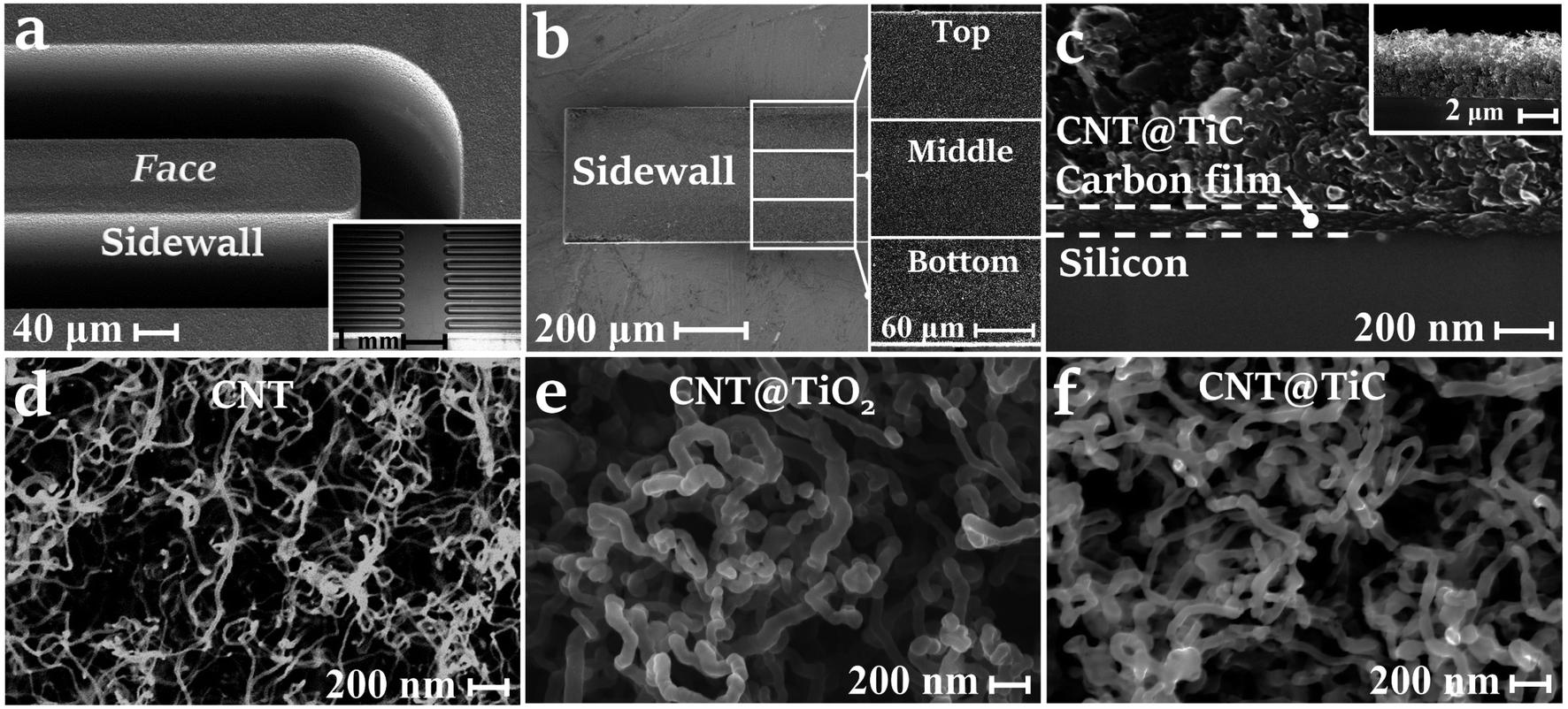 | ||
| Fig. 2 Structure characterizations of the proposed MSC by SEM. (a) Perspective view of the Si/C/CNT@TiC interdigits (inset: zoom-out structure); (b) side (inset: zoom-out images) and (c) cross-sectional (inset: zoom-out image). SEM images of the as-grown (d) CNT networks, (e) CNT@TiO2, and (f) CNT@TiC core–shell nanostructures. | ||
In addition, a high-resolution transmission electron microscopy (HRTEM) experiment was performed to characterize the lattice of the CNT@TiC core–shell structures, as shown in Fig. 3a. The overall size of the fiber is in agreement with the SEM results. While the zoom-in images in Fig. 3b confirm the existence of crystalline TiC, and the lattice fringes with interlayer spacing of 0.22 corresponds to the (200) plane of TiC, in agreement with the previously reported TiCs produced by carbonization of TiO2 and CNT.30,36 Furthermore, Raman spectroscopy was conducted to understand the composition of CNT@TiC core–shells before and after HF treatment, as shown in Fig. 3c. The week signal of TiO2 at 142 and 232 cm−1 disappears after the HF treatment, and the peaks at 265, 402 and 604 cm−1 appear in the other curve, and match well with the spectra reported for TiC nanostructures.37–39 This confirms that the synthesis technique is feasible in the absence of catalysts and toxic precursor at a moderate temperature of 1050 °C. The peaks at 1347 and 1585 cm−1 are corresponding to the D and G bands of CNT, respectively. Meanwhile, X-ray photoelectron spectroscopy (XPS) was carried out to study the chemical state of the elements of TiC, and the data was calibrated based on the C 1s line at 285.0 eV. The wide-scan spectra of CNT and CNT@TiC structures are illustrated in Fig. 3d. In comparison, Ti 2p region appears after in situ reduction by CNT@TiO2 at high temperature. The Ti 2p spectrum in Fig. 3e can be fitted into two peaks at 458.8 and 464.6 eV with an interval of 5.8 eV, which is consistent with reported results for TiO2,39–42 revealing that the Ti–C bond is not in the superficial layer. According to the C 1s spectrum in Fig. 3f, the peak at 284.5 eV corresponds to the sp2 hybridized carbon (C–C bonds), which is dominant in such composite.41
 | ||
| Fig. 3 Characterization of the Si/C/CNT@TiC electrode. (a) TEM image and (b) high magnification TEM microphotograph of CNT@TiC core–shells (inset: zoom-in images); (c) Raman spectra of Si/C, Si/C/CNT and Si/C/CNT@TiC structures; (d) wide-scan XPS patterns of Si/C/CNT and Si/C/CNT@TiC structures; XPS pattern in the regions of (e) Ti 2p and (f) C 1s for the Si/C/CNT@TiC structure. | ||
To evaluate the improvement in electrochemical performances contributed by CNT forests, the 3D Si/C and Si/C/CNT interdigital MSCs were tested using a two-electrode system. The CV curves of the Si/C and Si/C/CNT MSCs at scan rate of 5–100 mV s−1 are shown in Fig. 4a and b, respectively, both exhibiting symmetric shapes within a stable working potential window of 0–0.8 V with no redox peaks observed. In comparison, the Si/C/CNT MSC shows more rectangular CV curves and a larger enclosed area. The efficient electron pathways and increased surface area for charge/ion transport provided by the high aspect ratio CNT forests are believed to be crucial for the increased electronic and ionic conductivity.43 In addition, the GCD curves of the Si/C/CNT MSC at the current density of 10, 20, 40, 80 μA cm−2 are shown in Fig. 4c. The quasi-triangular shapes of the GCD curves indicate a good reversibility attributed by the well-matched electrode materials. In comparison, the electrodes with CNT show a relatively larger capacitance according to the CV curves (100 mV s−1) and GCD curves (10 μA cm−2), as shown in Fig. 4d and e. The increased capacitance results from the decreased inter-electrode distance for rapid ions diffusion and the increased surface area provided by CNT forests. As seen in Fig. 4f, in high frequency region of the EIS curves, MSCs exhibit a low electrolyte resistance (R0) value of 2.9 Ω for the Si/C MSC and 4.6 Ω for the Si/C/CNT MSC, implying a good electrical conductivity and excellent adherence between the network which consists of CNT forests, carbon-coated 3D current collector and silicon-based 3D substrate. In the low frequency region, the steeper curve of Si/C/CNT MSC shows a lower Warburg resistance (Zw), demonstrating an ideal EDLC behavior of the Si/C/CNT MSC.31
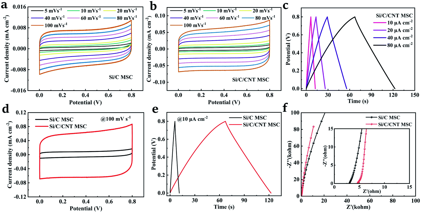 | ||
| Fig. 4 Electrochemical performance of the proposed MSCs with different electrodes. (a) CV curves for the Si/C MSC; (b) CV and (c) GCD curves for Si/C/CNT MSC; comparison of (d) CV curves for Si/C and Si/C/CNT MSCs at a scan rate of 100 mV s−1, (e) GCD curves at the current density of 10 μA cm−2 and (f) EIS curves for Si/C and Si/C/CNT MSCs. | ||
The electrochemical performances of the symmetric Si/C/CNT@TiC interdigital MSC were evaluated using a two-electrode and a three-electrode system cell, respectively, as demonstrated in Fig. 5, S1 and S2 (ESI†). It is believed that the functionalization process plays an essential role on the capacitive property of the CNT@TiC composite. Under the premise of the highest temperature allowed by the furnace and sufficient reactants, the carbothermal time was investigated as a key variable, and the result is shown in Fig. S1.† It is well accepted that a sufficient carbothermal time ensures complete reaction between CNT and TiO2. As a result, the final CNT@TiC-core–shell composite carbonized for 4 h shows higher electrical conductivity and better capacitive characteristics than those of 1 h and 2 h. Increasing the carbothermal time further will not produce any significant change in the electrochemical performances of the MSC. Therefore, the performance of Si/C/CNT@TiC electrodes carbonized by 4 h was investigated. As seen in Fig. 5a, symmetric CV curves at different scan rates indicate an excellent electrochemical reversibility of Si/C/CNT@TiC MSC. This result is in agreement with the nearly triangular GCD curves at the current density of 0.1–0.8 mA cm−2 (Fig. 5b). For comparison, the specific capacitance as a function of scan rate for all three symmetric MSCs are presented in Fig. 5c. The Si/C/CNT@TiC MSC shows the best rate capability (72.3% capacitance retention at 1 V s−1), as well as the highest specific capacitance of 3.71 F g−1 (7.42 mF cm−2) at 5 mV s−1 scan rate, which is higher than the reported MSCs such as the TiC-CDC MSC of 1.5 mF cm−2,44 the SWCNT/C/MnO2 MSC of 0.55 mF cm−2 and the ZnONR@TiN MSC of 1.24 mF cm−2.45,46 The good rate capability is due to the uniform formation of TiC shells on CNT core. The well-matched active material composite allows for an effective ion transportation in the electrolyte, and further shortens the ions diffusion distance. Furthermore, according to the EIS curves of the three MSCs shown in Fig. 5d, in the high frequency region, the R0 and amplitude of the semicircle can be maintained at a relatively low value compared to the reported 3D interdigitated MSCs.12–15 This fully elucidates the low charge transfer resistance and excellent interfacial contact between the TiC shells, CNT core and Si/C 3D framework.47 In the low frequency region, the CNT@TiC core–shells show a steeper slop, demonstrating a higher ion diffusivity and a lower Zw. The use of CNT and TiC both facilitate faster mass transport kinetics, showing a more ideal EDLC behaviour.
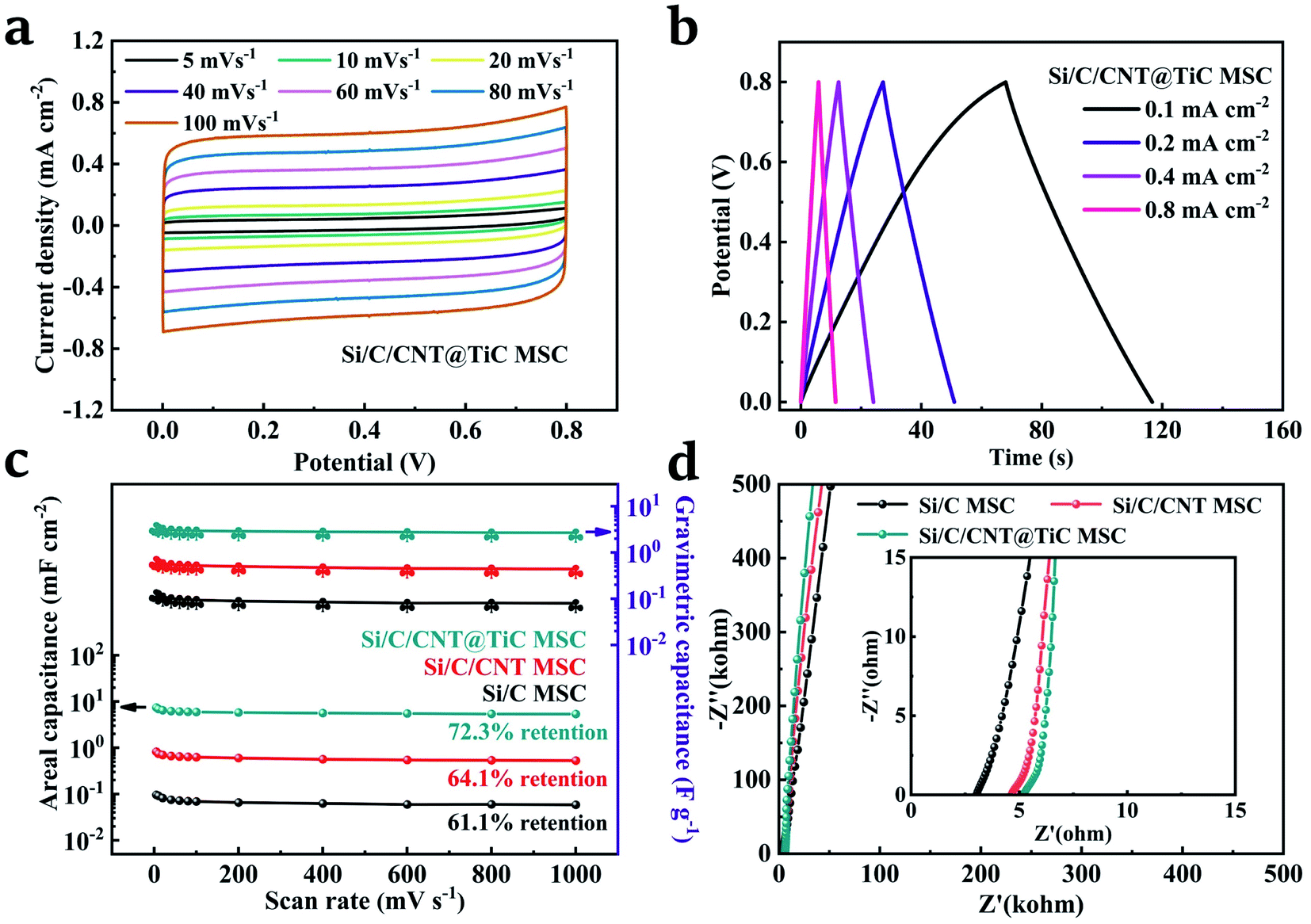 | ||
| Fig. 5 Electrochemical characterization of the Si/C/CNT@TiC MSC. (a) CV curves at the scan rate of 5–100 mV s−1 and (b) GCD curves at the current density of 0.1–0.8 mA cm−2 for the Si/C/CNT@TiC MSC in aqueous electrolyte. Comparison of (c) the specific capacitance as a function of scan rate (5–1000 mV s−1) and (d) EIS curves for the Si/C, Si/C/CNT and Si/C/CNT@TiC MSCs (zoom-in in inset). | ||
The Si/C/CNT/@TiC electrodes were assembled into a full device by using a glass mold and PVA/LiCl solid-state electrolyte. The symmetric CV curves are obtained at scan rate of 5–100 mV s−1, as shown in Fig. 6a. The quasi-rectangular shapes exhibit good electrochemical reversibility and EDLC behaviour for the all-solid-state Si/C/CNT@TiC MSC, which can be further supported by the GCD curves shown in Fig. 6b. The capacitance enhancement by the materials loading is calculated and exhibited in Fig. 6c. The as-prepared TiC shells and CNT forests produce approximately the same order of magnitude contribution to the overall capacitance of the MSC. The maximum specific capacitance is 5.01 mF cm−2 (2.51 F g−1) for Si/C/CNT@TiC, 0.86 mF cm−2 (0.72 F g−1) for Si/C/CNT and 0.12 mF cm−2 (0.17 F g−1) for Si/C. In addition, the gravimetric capacitance for the Si/C/CNT@TiC device is also gradually improved after each step as the active materials being loaded. The results are consistent with the MSCs in aqueous electrolyte, and similar results are obtained for the structures of Si/C/MnO2 in literature.15 More importantly, the significant increase in capacitance contributed by the deposition of active materials is particularly obvious in the 3D interdigital structure compared to bulk electrodes and interdigital in-plane MSCs. For example, the reported results for cotton cloth/TiC-based CNF@TiC, Ti3C2/CNT, ZnONR@TiN, CNT/MnO2 presented about a doubled increase in capacitance with the active material loaded by steps.30,46,48,49 Lastly, the long-term cycling stability of the all-solid-state Si/C/CNT@TiC full MSC was estimated by GCD at a current density of 3 mA cm−2. The capacitance retention and coulombic efficiency are presented in Fig. 6d. After 10000 continuous cycles, the capacitance still remains above 97.8% with a 99.7% coulombic efficiency, which is comparable to reported MnO2@MXene/CNT composites, layered Ti3C2 electrodes and TiC/C nanofibers electrodes.50–52 The inset of Fig. 6d shows the CV curves at 100 mV s−1 scan rate and Nyquist plots before and after cycling for comparison. The consistent shapes demonstrate an excellent reversibility, mechanical stability and cycling stability of the Si/C/CNT@TiC MSC. We further evaluated the energy and power densities of the proposed MSCs, as shown in Fig. 6e. Due to the contribution of CNT and TiC, the energy density of as prepared MSC increases, and the Si/C/CNT@TiC MSC offers the highest energy density of 0.45 μW h cm−2 (0.22 W h kg−1) at the scan rate of 5 mV s−1, which is comparable to the 3D interdigitated Si/C/MnO2 MSC of 1.33 μW h cm−2 and ZnONR/TiN MSC of 0.24 W h kg−1,15,46 and higher than the TiC-CDC MSC of 0.83 μW h cm−2 and SiNW/SiC MSC of 0.24 μW h cm−2 reported before.53,54 Impressively, the Si/C/CNT@TiC MSC shows a significant increase in capacitive performance, due to the rationale design of the 3D hybrid architecture (optical image shown in Fig. 6f), so that the electrodes possess a high aspect ratio and excellent electrical conductivity.
 | ||
| Fig. 6 Electrochemical performance of the well-packaged all-solid-state Si/C/CNT@TiC MSC devices. (a) CV curves at the scan rate of 5–100 mV s−1; (b) GCD curves at the current density from 0.4–2 mA cm−2; (c) comparison of the specific capacitance as a function of the scan rate (5–1000 mV s−1) for three devices; (d) long-time cycling performance (CV curves and Nyquist plots before and after cycling in inset); (e) Ragone plots of the three devices. (f) Optical image of the MSC in a well-designed glass mold. | ||
High energy density EDL capacitors with good electronic/ionic conductivity can achieve superior frequency response, and are promising devices for the application in AC line filtering.55–57 The frequency responses are shown in Fig. S3,† exhibiting a great potential for AC filtering applications. Therefore, the packaged Si/C, Si/C/CNT and Si/C/CNT@TiC MSCs are integrated into a full-wave bridge rectifier circuit (Fig. 7a) for the conversion of AC to DC. The full-wave rectifier bridge circuit consists of four same diodes (1N4007) and a 1 kΩ load resistance connected in parallel with the fabricated MSCs in order to reduce the ripple of the output voltage. A stable operating voltage window of 0.8 V was provided to 3D MSCs by applying a 60 Hz AC input with 2 V amplitude, as shown in Fig. 7b. The DC output voltage with a small ripple coefficient of 1.5% (17.7 mV with an average output potential of 0.589 V) was obtained by Si/C/CNT@TiC MSC as shown in Fig. 7b, which is comparable to the reported high-frequency MSCs.55,58 More importantly, the Si/C/CNT@TiC full device shows a lower overall capacitance but smoother output voltage than the previously reported Si/C/MnO2 full device (Fig. 7c),15 validating the well-matched active material with lower resistance and faster electronic/ionic transport efficiency of the proposed MSC. The ripple of the output voltage can be further reduced by connecting full devices in parallel. The series-parallel characteristics of the full devices are shown in Fig. 7d and S4.† It is seen that as the number of paralleled devices increase, the capacitance increases, and accordingly more stable DC output can be obtained. Therefore, we believe that the as prepared Si/C/CNT@TiC MSC can be applied to AC/DC power conversion and low-pass filtering applications.
 | ||
| Fig. 7 The low-pass filtering circuit and on-chip application based on the 3D MSCs (a) optical image of the full-wave bridge rectifier circuit; (b) output of the circuit with Si/C, Si/C/CNT and Si/C/CNT@TiC MSCs; (c) zoomed-in output of the circuit and comparison with reported results (inset: circuit diagram); (d) output of the circuit with Si/C/CNT@TiC full device connected in parallel. | ||
Experimental
Preparation of Si/C/CNT@TiC MSC
The fabrication process of 3D Si framework and carbon film have been reported in previous studies.15 The DRIE-etched 400 μm-thick Si framework are composed of 50 pairs of interdigits with a width of 100 μm and a length of 3000 μm for each finger. CNT with a mass loading of 0.16 mg was fabricated by CVD method. A 20 nm Ni film as catalyst was deposited twice by magnetron sputtering at a current of 1 A in Ar atmosphere (30 sccm, 0.3 Pa) to ensure uniform deposition of CNT. The CVD reaction was conducted at 700 °C for 20 min under an argon/hydrogen (200/50 sccm) gas mixture atmosphere with flowing ethanol as the carbon source in a tube furnace. Next, a uniform ALD-TiO2 film (∼25 nm) was fabricated on the CNT forests with Tetrakis Dimethylamino Titanium (TDMAT) as Ti precursor at a chamber temperature of 200 °C. The as prepared CNT@TiO2-core–shell composite was then carbonized in a tube furnace at 1050 °C for 1, 2, 4 h, respectively. Lastly, the well-controlled and crisscrossed TiC shells are exposed after HF etching to remove the remaining reactants. The deposited specific mass loading of C/CNT@TiC was approximately 0.60 mg on the electrode fingers with an active area of 0.3 cm2. The as-prepared Si/C/CNT@TiC electrode array was assembled onto a well-designed glass mold and electrically connected to an electrochemical workstation, detailed in previous studies.15Material characterizations
The microstructure and surface elementals of 3D interdigits MSCs were characterized by scanning electron microscopy (SEM, ZEISS), high-resolution transmission electron microscopy (HRTEM, FEI TF20) and X-ray photoelectron spectroscopy (XPS, AXIS-ULTRA DLD-600W). Raman spectroscopy system (inVia Reflex, Renishaw) with a laser wavelength of 532 nm was employed to obtain the Raman spectra of the samples. The spectra of the sample were measured twice with a dwell time of 10 s at each point and then averaged.Electrochemical characterization
Cyclic voltammetry (CV), galvanostatic charge–discharge (GCD) and electrochemical impedance spectroscopy (EIS) curves of the 3D MSCs were performed using an electrochemical workstation (CH Instruments Inc., CHI660E) with both two-electrode and three-electrode configurations in 1 M Na2SO4 aqueous electrolyte. The EIS was conducted in the frequency range of 0.01–10 kHz at 5 mV s−1 voltage amplitude. Electrical connections to the MSC during the measurement was similar to that reported by Wang et al.15 The specific capacitance (F cm−2 or F g−1) of the electrode was calculated using| Cs = ∫I(V)dV/(2νSΔV) | (1) |
| E = 1/2(CsΔV2) = PΔt | (2) |
| rc = Δu/2U | (3) |
Conclusions
In summary, we have demonstrated a 3D interdigital Si framework with carbon film as current collector and CNT@TiC as active material fabricated by DRIE, sputtering, ALD and carbonization. With a rationale design, the as-prepared Si/C/CNT@TiC MSC exhibited a high electrical conductivity and mechanical stability, and showed an 8 times increment in areal capacitance after the material coating at each step. The all-solid-state Si/C/CNT@TiC MSC with an outstanding EDLC behaviour delivered a high specific capacitance and long cycling life (>10000 cycles). In addition, the well-packaged on-chip MSC with CNT@TiC on 3D interdigital silicon scaffold demonstrated a superior AC line-filtering performance with a low ripple coefficient of 1.5%, facilitating the understanding of electron/ion transport mechanisms in the 3D high aspect ratio interdigits, and indicating great potential of metal-carbide for the energy storage and filtering applications.
Conflicts of interest
There are no conflicts to declare.Acknowledgements
This work was partially supported by the National Natural Science Foundation of China [Grant No. 51902112].Notes and references
- M. Beidaghi and Y. Gogotsi, Energy Environ. Sci., 2014, 7, 867–884 RSC.
- A. González, E. Goikole, J. A. Barrena and R. Mysyk, Renewable Sustainable Energy Rev., 2016, 58, 1189–1206 CrossRef.
- C. Lethien, J. L. Bideau and T. Brousse, Energy Environ. Sci., 2019, 12, 96–115 RSC.
- Z. Zhu, R. Kan, S. Hu, L. He, X. Hong, H. Tang and W. Luo, Small, 2020, 16, 2003251 CrossRef CAS PubMed.
- B. G. Choi, M. H. Yang, W. H. Hong and J. W. Choi, ACS Nano, 2012, 6, 4020–4028 CrossRef CAS PubMed.
- P. Yang, X. Xiao, Y. Li, Y. Ding and P. Qiang, ACS Nano, 2013, 7, 2617–2626 CrossRef CAS PubMed.
- L. He, H. Liu, W. Luo, W. Zhang, X. Liao, Y. Guo, T. Hong, H. Yuan and L. Mai, Appl. Phys. Lett., 2019, 114, 223903 CrossRef.
- W. Yang, Y. Zhu, Z. Jia, L. He, L. Xu, J. Meng, M. Tahir, Z. Zhou, X. Wang and L. Mai, Adv. Energy Mater., 2020, 10, 2001873 CrossRef CAS.
- N. A. Kyeremateng, T. Brousse and D. Pech, Nat. Nanotechnol., 2017, 12, 7–15 CrossRef CAS PubMed.
- H. Liu, Y. Xie, J. Li, Z. Sun, J. Liu, K.-s. Moon, L. Lu, Y. Chen, Y. Tang and X. Chen, Chem. Eng. J., 2021, 404, 126375 CrossRef CAS.
- H. Liu, Y. Xie, J. Liu, K.-s. Moon, L. Lu, Z. Lin, W. Yuan, C. Shen, X. Zang and L. Lin, Chem. Eng. J., 2020, 393, 124672 CrossRef CAS.
- C. Shen, X. Wang, W. Zhang and F. Kang, J. Power Sources, 2011, 196, 10465–10471 CrossRef CAS.
- J. Pu, X. Wang, T. Zhang, S. Li, J. Liu and K. Komvopoulos, Nanotechnol, 2015, 27, 045701 CrossRef PubMed.
- W. Sun, R. Zheng and X. Chen, J. Power Sources, 2010, 195, 7120–7125 CrossRef CAS.
- Y. Wang, L. Sun, D. Xiao, H. Du, Z. Yang, X. Wang, L. Tu, C. Zhao, F. Hu and B. Lu, ACS Appl. Mater. Interfaces, 2020, 12, 43864–43875 CrossRef CAS PubMed.
- L. Liu, H. Zhao and Y. Lei, InfoMat, 2019, 1, 74–84 CrossRef CAS.
- Q. Wang, J. Yan and Z. Fan, Energy Environ. Sci., 2016, 9, 729–762 RSC.
- F. Wang, X. Wu, X. Yuan, Z. Liu, Y. Zhang, L. Fu, Y. Zhu, Q. Zhou, Y. Wu and W. Huang, Chem. Soc. Rev., 2017, 46, 6816–6854 RSC.
- C. Yin, L. He, Y. Wang, Z. Liu, G. Zhang, K. Zhao, C. Tang, M. Yan, Y. Han and L. Mai, RSC Adv., 2016, 6, 43436–43441 RSC.
- T. Huang, K. Jiang, D. Chen and G. Shen, Chin. Chem. Lett., 2018, 29, 553–563 CrossRef CAS.
- N. Li, J. Peng, W.-J. Ong, T. Ma, Arramel, P. Zhang, J. Jiang, X. Yuan and C. Zhang, Matter, 2021, 4, 377–407 CrossRef CAS.
- Q. Jiang, C. Wu, Z. Wang, A. C. Wang, J.-H. He, Z. L. Wang and H. N. Alshareef, Nano Energy, 2018, 45, 266–272 CrossRef CAS.
- K. Kannan, K. K. Sadasivuni, A. M. Abdullah and B. Kumar, Catalysts, 2020, 10, 495 CrossRef CAS.
- Y. Xie, H. Zhang, H. Huang, Z. Wang, Z. Xu, H. Zhao, Y. Wang, N. Chen and W. Yang, Nano Energy, 2020, 74, 104928 CrossRef CAS.
- J. Li, H. Wang and X. Xiao, Energy Environ. Mater., 2020, 3, 306–322 CrossRef CAS.
- D. Xiong, X. Li, Z. Bai and S. Lu, Small, 2018, 14, e1703419 CrossRef PubMed.
- C.-S. Yang, Z. Sun, Z. Cui, T. Zhang, F.-L. Jianga and J.-W. Denga, Energy Storage Mater., 2020, 30, 59–66 CrossRef.
- X. Sun, Y. Han, S. Cao, P. Qiu and W. Lu, J. Mater. Sci. Technol., 2017, 33, 1165–1171 CrossRef CAS.
- F. Saba, S. A. Sajjadi, M. Haddad-Sabzevar and F. Zhang, Ceram. Int., 2018, 44, 7949–7954 CrossRef CAS.
- X. Xia, Y. Zhang, D. Chao, Q. Xiong, Z. Fan, X. Tong, J. Tu, H. Zhang and H. J. Fan, Energy Environ. Sci., 2015, 8, 1559–1568 RSC.
- B. Cao, Y. Chen, D. Li, L. Yin and Y. Mo, ChemSusChem, 2016, 9, 3338–3344 CrossRef CAS PubMed.
- D.-W. Lee, S. V. Alexandrovskii and B. K. Kim, Mater. Lett., 2004, 58, 1471–1474 CrossRef CAS.
- L. Sun, X. Wang, Y. Wang, D. Xiao, W. Cai, Y. Jing, Y. Wang, F. Hu and Q. Zhang, Front. Chem., 2019, 7, 512 CrossRef CAS PubMed.
- M. Létiche, E. Eustache, J. Freixas, A. Demortière, V. D. Andrade, L. Morgenroth, P. Tilmant, F. Vaurette, D. Troadec, P. Roussel, T. Brousse and C. Lethien, Adv. Energy Mater., 2017, 7, 1601402 CrossRef.
- E. Eustache, C. Douard, A. Demortière, V. D. Andrade, M. Brachet, J. L. Bideau, T. Brousse and C. Lethien, Adv. Mater. Technol., 2017, 2, 1700126 CrossRef.
- L. Zhang, M. S. Tse, O. K. Tan, Y. X. Wang and M. Han, J. Mater. Chem. A, 2013, 1, 4497–4507 RSC.
- V. Kiran, K. Srinivasu and S. Sampath, Phys. Chem. Chem. Phys., 2013, 15, 8744–8751 RSC.
- B. H. Lohse, A. Calka and D. Wexler, J. Appl. Phys., 2005, 97, 114912 CrossRef.
- L. Zhang and R. V. Koka, Mater. Chem. Phys., 1998, 57, 23–32 CrossRef CAS.
- O. O. Abegunde, E. T. Akinlabi and O. P. Oladijo, Appl. Surf. Sci., 2020, 520, 146323 CrossRef CAS.
- W. S. Kim, S. Y. Moon, J. H. Lee, S. Y. Bang, B. G. Choi, H. Ham, T. Sekino and K. B. Shim, Nanotechnol, 2010, 21, 055608 CrossRef PubMed.
- I. Iatsunskyi, M. Kempiński, G. Nowaczyk, M. Jancelewicz, M. Pavlenko, K. Załęski and S. Jurga, Appl. Surf. Sci., 2015, 347, 777–783 CrossRef CAS.
- Z. Yu, L. Tetard, L. Zhai and J. Thomas, Energy Environ. Sci., 2015, 8, 702–730 RSC.
- P. Huang, M. Heon, D. Pech, M. Brunet, P.-L. Taberna, Y. Gogotsi, S. Lofland, J. D. Hettinger and P. Simon, J. Power Sources, 2013, 225, 240–244 CrossRef CAS.
- L. Sun, X. Wang, K. Zhang, J. Zou and Q. Zhang, Nano Energy, 2016, 22, 11–18 CrossRef CAS.
- Y. Wang, L. Sun, P. Song, C. Zhao, S. Kuang, H. Liu, D. Xiao, F. Hu and L. Tu, J. Power Sources, 2020, 448, 227415 CrossRef CAS.
- A. Lewandowski, A. Olejniczak, M. Galinski and I. Stepniak, J. Power Sources, 2010, 195, 5814–5819 CrossRef CAS.
- P. Yan, R. Zhang, J. Jia, C. Wu, A. Zhou, J. Xu and X. Zhang, J. Power Sources, 2015, 284, 38–43 CrossRef CAS.
- B. Dousti, Y. I. Choi, S. F. Cogan and G. S. Lee, ACS Appl. Mater. Interfaces, 2020, 12, 50011–50023 CrossRef CAS PubMed.
- Q. Liu, J. Yang, X. Luo, Y. Miao, Y. Zhang, W. Xu, L. Yang, Y. Liang, W. Weng and M. Zhu, Ceram. Int., 2020, 46, 11874–11881 CrossRef CAS.
- S. Lin and X. Zhang, J. Power Sources, 2015, 294, 354–359 CrossRef CAS.
- Y. Ren, J. Dai, B. Pang, X. Liu and J. Yu, Electrochim. Acta, 2015, 176, 402–409 CrossRef CAS.
- F. Liu, A. Gutes, I. Laboriante, C. Carraro and R. Maboudian, Appl. Phys. Lett., 2011, 99, 112104 CrossRef.
- L. Zhang, D. DeArmond, N. T. Alvarez, R. Malik, N. Oslin, C. McConnell, P. K. Adusei, Y. Y. Hsieh and V. Shanov, Small, 2017, 13, 1603114 CrossRef PubMed.
- Q. Jiang, N. Kurra, K. Maleski, Y. Lei, H. Liang, Y. Zhang, Y. Gogotsi and H. N. Alshareef, Adv. Energy Mater., 2019, 9, 1901061 CrossRef.
- Y. Rangom, X. Tang and L. F. Nazar, ACS Nano, 2015, 9, 7248–7255 CrossRef CAS PubMed.
- K. Sheng, Y. Sun, C. Li, W. Yuan and G. Shi, Sci. Rep., 2012, 2, 247 CrossRef PubMed.
- S. Xu, W. Liu, B. Hu and X. Wang, Nano Energy, 2019, 58, 803–810 CrossRef CAS.
Footnote |
| † Electronic supplementary information (ESI) available. See DOI: 10.1039/d1ra08456a |
| This journal is © The Royal Society of Chemistry 2022 |