
 Open Access Article
 This Open Access Article is licensed under a Creative Commons Attribution-Non Commercial 3.0 Unported Licence
In situ construction of a Te/CsPbBr3 heterojunction for self-powered photodetector
Jie Zhangab and
Jiaojiao Liu *ab
*ab
aCollege of Electronic and Information Engineering, Changshu Institute of Technology, Changshu 215500, China. E-mail: zj2016@cslg.edu.cn; liujiaojiao@cslg.edu.cn
bSuzhou Key Laboratory of Advanced Lighting and Display Technologies, China
First published on 20th January 2022
Abstract
In this study, CsPbBr3 particles were prepared by a simple solvent evaporation method in ambient environment; the p–n heterojunction formed by CsPbBr3 particles on the surface of a single long Te wire was used to construct a high-performance Te/CsPbBr3 photodetector. Compared with CsPbBr3 PDs, the Te/CsPbBr3 photodetector showed improved photocurrent, and exhibited characteristics of excellent self-powered performance, broad-spectrum response (UV-visible), and ultra-fast response speed (trise = 0.09 ms). In addition, under zero bias and upon 540 nm light irradiation, the device had good responsivity (0.35 mA W−1), high photosensitivity (up to 100 on/off ratio), and a detectivity of 1.42 × 10¹⁰ Jones. This study provides insight into the possibility of manufacturing high-performance self-powered photodetectors through a simple in situ construction of heterojunctions.
1. Introduction
Photodetectors (PDs) can convert optical signals into electrical signals by the photoelectric effect. By analyzing the electrical signals, it is easy to derive the optical signal information and detect optical radiation. PDs have applications in environmental monitoring, environmental sensors, spectrum analysis, communications, imaging, etc.1–5 In general, PDs need an external power supply to work, but self-powered PDs take advantage of the photovoltaic effect of the p–n junction, heterojunction, or Schottky junction, and can work under zero bias.6 Self-powered PDs are energy-saving, safe, and stable, and have great application potential.7–9 Therefore, particularly in the face of the global energy crisis, the electronic equipment industry is urgently pursuing this self-powered feature. This study focuses on the manufacture of self-powered PDs through the construction of heterojunctions.Tellurium (Te) is a common p-type semiconductor with a band gap of 0.35 eV.10 Due to anisotropy during the growth of Te crystals, they can form one-dimensional nanostructures. One-dimensional Te crystals are called Te nanowires, and the synthesis process is simple, fast, and high-yielding. In addition, Te nanowires also have excellent photoelectric properties. Te nanowires have applications in gas sensing, nonlinear optical response devices, optoelectronic devices, thermoelectric devices, piezoelectric devices, photonic crystals, field-effect devices, and infrared acousto-optic deflectors, etc.11,12 Considering Te nanowires have a high specific surface area, clear charge transfer pathway, and good surface adhesion, it is a promising candidate for constructing high-performance self-powered PDs with high photosensitivity, high responsiveness, and excellent performance.13 Te wire is very suitable for constructing heterojunction photodetectors, and its composite device may have excellent self-powered performance.
The organic–inorganic hybrid perovskite has received considerable attention recently due to its excellent photoelectric properties. These include an adjustable direct band gap, high electron mobility, long electron holes, simple processing technology, easy integration with various semiconductor materials.14,15 However, the instability, humidity, and high temperature of organic lead halide perovskites and its composites under continuous irradiation have severely hindered its long-term application in commercial development.16 CsPbBr3 is a kind of organic–inorganic perovskite with good stability and good light detection performance. The PDs based on perovskite crystals have been widely used, with characteristics of high detectivity and fast response speed.17,18 Due to the high electron mobility and low exciton binding energy of CsPbBr3, considerable research has been conducted on its photoelectric properties.19 In addition, CsPbBr3 particle has high stability, excellent optical properties, and can be combined with other materials for optoelectronic components.20 Fang et al. reported that millimeter-sized CsPbBr3 was prepared by a simple solution evaporation method to form p-CuI/n-CsPbBr3 heterojunctions. The resulting device exhibited good rectification characteristics and excellent self-powering performance upon 540 nm light illumination.21 Fang et al. also reported that a controllable combination of CsPbBr3 and SnO2 of different sizes was formed by chemical deposition, and the formed optoelectronic device achieved a dual spectral response. Upon 320, 520 nm light illumination, both showed good self-powered characteristics.22 However, when PDs about Te and CsPbBr3 composite are unreported, we can use a simple method to construct Te/CsPbBr3 heterojunction and study its performance.
In this study, CsPbBr3 particles were prepared by a simple solvent evaporation method in ambient environment, and the p–n heterojunction formed by CsPbBr3 particles on the surface of a single long Te wire was used to construct a high-performance Te/CsPbBr3 photodetector. The as-fabricated p-Te/n-CsPbBr3 heterojunction device worked stably as a self-powered UV PD with broad-spectrum response (UV-visible), and exhibited excellent self-powered characteristics under 540 nm light irradiation, such as high photocurrent (near 1 nA, good responsivity (0.35 mA W−1)), high photosensitivity (up to 100 on/off ratio), detectivity of 1.42 × 10¹⁰ Jones per W and fast response speed (trise = 0.09 ms). This work introduces a simple method for constructing heterojunction devices in situ and provides insights into manufacturing high-performance self-powered PDs.
2. Experimental section
2.1 CVD method to prepare Te wire
Te powder was placed in the middle of the horizontal tube furnace, the horizontal tube furnace was vacuumed to less than 1 mTorr, and filled with a carrier gas for cleaning. After repeating twice, the carrier gas was passed and a mechanical pump was used to maintain the pressure in the furnace tube at 10–15 torr. The cleaned Te substrate was then placed downwind from the evaporation source, in the middle of the horizontal tube furnace and at a distance of 25 cm to 28 cm from the middle of the furnace body, and the horizontal tube furnace heated. The temperature of the evaporation source in the tube was increased to 480 °C, and this temperature was maintained for 90–150 min. During the reaction, carrier gas was passed. After the reaction finished, the carrier gas was passed continually for natural cooling.2.2 Preparation of the Te/CsPbBr3 heterojunction
All the chemicals were purchased from Aladdin and used directly without further processing. The Te wire prepared by CVD was placed on a clean glass substrate, and the 0.45 M PbBr2 (99.999%) dimethylformamide (DMF) precursor solution was dropped around the Te wire onto the glass substrate (Fig. 1a). As DMF evaporated, a series of PbBr2 milliwires (MWs) were formed on the Te surface. 0.45 M CsBr (99.9%) methanol solution was immersed in half of the Te–PbBr2 (MWs) to form CsPbBr3 particles on the Te wire surface. It was heated for 30 min under ambient conditions to form a Te/CsPbBr3 heterojunction (Fig. 1a). The Te/CsPbBr3 heterojunction was cleaned with isopropanol before use. Two small pieces of indium paste were coated on the surface of the composite as electrodes to construct Te/CsPbBr3. Electrode diameter and length were about 0.2 × 0.05 cm and the effective area was about 0.001 cm2. | ||
| Fig. 1 (a) Schematic of the preparation process of the Te/CsPbBr3 heterojunction. The photographs of the as-prepared Te wire and the Te/CsPbBr3 heterojunction (b) and (c). (d) Optical microscope image of the Te/CsPbBr3 heterojunction. | ||
2.3 Characterization
A field-emission scanning electron microscope (FE-SEM, Zeiss Sigma) was used to characterize sample morphologies. X-ray diffraction (XRD) patterns were collected on a Bruker D8-A25 diffractometer using Cu Kα radiation (λ = 1.5405 Å) in the 2θ range from 10° to 70°. X-ray photoelectron spectroscopy (XPS, PerkinElmer PHI 5000C ESCA system equipped with a hemispherical electron energy analyzer) was utilized experimentally to investigate the composition and chemical state of the samples. The binding energy for the C 1s peak at 285 eV was used as the reference for calibration. The photoelectric performance was characterized by a program-controlled semiconductor characterization system (Keithley 4200, USA). Time-resolved responses of the device were measured with a YAG:Nd laser in the pulse duration range of 3–5 ns (Continuum Electro-Optics, MINILITE II, 355 nm), an oscilloscope (Tektronix MSO/DPO5000), and a 1 GΩ resistor. The light intensity was measured with a NOVA II power meter (OPHIR Photonics). All measurements were performed at room temperature.3. Results and discussion
A schematic of the process of forming a heterojunction is shown in Fig. 1a. It can be seen that Te wires are crystals with metal glossy and only a few millimeters long (Fig. 1b). The surface of the Te wire was covered by CsPbBr3 particles, which caused the color of the Te wires to change to yellow and formed a Te/CsPbBr3 composite material. Fig. 1c is a photo of the heterojunction used in the experiment. Fig. 1d is an optical microscope photo of the end of the Te wire covered with CsPbBr3 particles. It was observed that pure CsPbBr3 particles aggregate on the Te surface, and the long Te wire can easily be assembled into different heterostructures. As the preparation process of the Te/CsPbBr3 heterojunction is simple, it has potential applications in the field of basic research.X-ray diffraction (XRD) patterns were used to determine the crystalline properties of single Te wires and CsPbBr3 particles. The Te wires were synthesized by the chemical vapor deposition method. CsPbBr3 particles were obtained by a simple solvent evaporation method. The detailed preparation process is discussed in the experimental part. As shown in Fig. 2a, the strong and sharp diffraction peak of a single Te wire at 27.5° proves the high crystal quality, which corresponds to the (101) crystal plane of hexagonal Te with lattice parameters of a = b = 4.458 Å and c = 5.927 Å (JCPDF no. 36-1452). The as-prepared high-quality Te wires are a promising candidate to be integrated with other semiconductor materials in various device structures. Fig. 2b exhibits the diffraction peaks of the CsPbBr3 particles, which match well with monoclinic cesium lead bromide with lattice parameters of a = 9.843 Å, b = 4.127 Å, and c = 6.874 Å, (JCPDF no. 54-0751), and confirm the crystallinity and purity of the as-obtained sample. The main diffraction peaks of CsPbBr3 particles located at 15.05°, 21.68°, 23.84°, 30.79°, 37.41°, 42.97° are attributed to the (001), (010), (110), (002), (102), (020) crystal facets, respectively, of the CsPbBr3 particles. The obvious peak at 2θ of 30.8° corresponds to the (002) crystal plane of CsPbBr3, indicating that the crystal exposed surface is the (002) plane. The diffraction peaks at 12.7° and 18.2° are derived from PbBr2 MWs (these two peaks are not marked in Fig. 2b). We used a two-step method to prepare CrPbBr3 particles. A part of the PbBr2 crystals generated in the first step was not completely converted into CrPbBr3 particles, indicating the presence of PbBr2 impurity peaks. These characteristics indicate that Te wires and CsPbBr3 particles have good crystallinity. To investigate the composition and electronic states of the as-prepared CsPbBr3 crystals, X-ray photoelectron spectroscopy (XPS) measurements were performed using element C for calibration. Fig. 2c shows the XPS spectrum of the CsPbBr3 sample. Fig. 2d–f presents the spectra of elements in the CsPbBr3 sample and Fig. 2d shows that the binding energy spectrum (XPS) of 725.4 eV corresponds to Cs 3d5/2. The two nearby binding energy peaks at 139.5 eV and 144.4 eV were attributed to Pb 4f7/2 and Pb 4f5/2, respectively, revealing the existence of Pb2+ in CsPbBr3 samples (Fig. 2e). The binding energy peaks located at 69.9 eV can be attracted to the spin–orbit splitting photoelectron of Br 3d5/2 (Fig. 2f). The results further proved the coexistence of the elements Cs, Pb, and Br. The Te wires and CsPbBr3 crystals obtained by collecting all these features have good crystallinity.
 | ||
| Fig. 2 XRD patterns (a) Te wire (b) CsPbBr3 particles, XPS spectra (c) CsPbBr3 (d) Cs 3d (e) Pb 4f (f) Br 3d. | ||
To explore the potential of PD, and study its photoelectric performance and self-powered properties, CsPbBr3 particles were used to integrate onto the surface of Te wire to form a Te/CsPbBr3 composite. The schematic of the Te/CsPbBr3 PD is shown in Fig. 3a. Fig. 3b shows the current–voltage (I–V) curve of a single Te/CsPbBr3 heterojunction under dark and upon 500, 400, and 300 nm light illumination under the bias of 3 V. Te/CsPbBr3 PDs exhibited different photocurrent and dark currents, indicating that it had acquired photoelectric characteristics. Under the illumination of 500 nm at 3 V, the photocurrent of the Te/CsPbBr3 device could reach 28 nA, which was about 223 times that in dark. Under 0 V and 500 nm light illumination, the relatively high photocurrent of 3.7 nA indicates that the hybrid device can be used as a self-powered PD to detect light without additional energy consumption. The effect of self-powered devices is mainly based on the photovoltaic effect of p-Te and n-CsPbBr3 heterojunction. The photocurrent of the Te/CsPbBr3 device is two orders of magnitude larger than the dark current, which indicates that the device has good photoresponse characteristics under illumination.
 | ||
| Fig. 3 (a) Schematic of the Te/CsPbBr3 PD; Typical I–V curves for different device under dark and illumination of 500 nm; (b) the Te/CsPbBr3 PD (c) CsPbBr3 particles (d) Te wire. | ||
For comparison, the I–V curves of the pure CsPbBr3 particle device and the Te device are shown in Fig. 3c and d. The pure CsPbBr3 device has a photoelectric response, and the Te device has no photoelectric characteristics, but the photocurrent and dark current values are not much different, and the dark current is very small at 0 V. This shows that neither the CsPbBr3 device nor the Te device can produce self-powered behavior. Te is a p-type semiconductor material with high hole mobility and carrier concentration, which is generally used as a hole transport layer.23 CsPbBr3 particles is an n-type semiconductor with high carrier mobility, which can balance the electron–hole diffusion length in the range of visible light.24,25 This means that the self-powered behavior of the Te/CsPbBr3 device originates from the p–n junction formed by p-Te and n-CsPbBr3. The Te/CsPbBr3 composite device has a better photoelectric and self-powered performance than the CsPbBr3 device. The Te device can also be used as PDs, but the on-off ratio is so small that our equipment cannot measure it.
To further detect the response characteristics of Te/CsPbBr3 PD, we checked current–time (I–t) for different bias voltages (3 V, 0.5 V, and −0.5 V) under 500, 400, and 300 nm light (Fig. 4). For comparison, we tested the I–t curve of the CsPbBr3 device under 500 nm light and Te/CsPbBr3 PDs under 500, 400, 300 nm light at 3 V, as shown in Fig. 4a. For the CsPbBr3 device, the output current rose from nearly zero to 60 pA when the ultraviolet light was switched on, and attenuated to 3 pA when the light was switched off. When the light (500, 400, and 300 nm) is turned on at 3 V, the photocurrent reached 12 nA, 8 nA, and 4 nA, the dark current was 0.1 nA, and the maximum on/off ratio was 120. We note that when compared with the CsPbBr3 device, Te/CsPbBr3 PDs have better photosensitivity and the photocurrent is relatively smoother when starting and stopping the illumination, indicating that the photocurrent of the PDs is less sensitive to the capacitive current. Different biases (−0.5 V and 0.5 V) were applied according to their open-circuit voltages (Fig. 3b), as shown in Fig. 4b. Interestingly, the photocurrent and dark current of Te/CsPbBr3 PD at 0.5 V were higher than −0.5 V, and the on/off ratio of the device was higher too. This may have been caused by the photovoltaic effect, and the ratio of light to dark current shown in Fig. 3b. The open-circuit voltage of the device was about 0.5 V, which has a similar dark current but a higher photocurrent and on/off ratio than at −0.5 V. The I–t curve shows that the on/off switch is repeatable and stable under a negative bias and that there is no obvious photocurrent decay cycle. Te/CsPbBr3 PDs under positive and negative biases have photoelectric properties similar to conventional UV PDs.26
 | ||
| Fig. 4 (a) I–t curves of the CsPbBr3 device and Te/CsPbBr3 PDs upon different light illumination under 3 V (b) the Te/CsPbBr3 (0.5 V and −0.5 V) PDs upon 500 nm light illumination. | ||
The Te/CsPbBr3 PDs exhibited an obvious photoresponse at the bias of 0 V upon different light illumination, indicating that the device can be used as a self-powered PD. Fig. 5a shows the time-dependent current (I–t) tests under 500, 400, and 300 nm light at 0 V. Reliability and rapid response to light illumination are essential for high-performance PDs. The repeatability and the speed of response to light are two important factors to measure the performance of PDs. The device showed high stability and repeatability in multiple switching cycles under 500, 400, and 300 nm light, with no obvious attenuation in each cycle. When the light was switched on and off without an external power source, the photocurrent of the device rapidly increased to a steady-state, and then rapidly decreased. This indicates that the built-in electric field near the heterojunction caused the electron–hole pair to quickly separate. In the absence of an external bias, the photosensitivity of the device (Iph/Id) under 500, 400, and 300 nm illumination was respectively 100, 70, 50. The maximum photocurrent could reach 1 nA under 0 V upon 500 nm light. In addition, the photocurrent remained stable during continuous illumination, indicating that the device can operate efficiently and stably without an external power supply. To better illustrate the time-resolved characteristics of the device, a rapid response measurement system was applied. The pulse response of the device is shown in Fig. 5c and d. In the application of this system, a pulsed YAG:Nd laser was used as the light source, and an oscilloscope recorded the voltage variation of series resistance with time. When the pulsed laser irradiated PDs, the concentration of photogenerated carriers increased and the resistance decreased, leading to the rise in the partial pressure on the resistance. At a bias of 0 V, the optical response of the device was very fast, and the oscilloscope captured the photovoltaic voltage change on the device after local illumination. Fig. 5b shows a laser pulse of 0 V in response. The ten cycles of Te/CsPbBr3 PD impulse response confirm the stability and repeatability of the device. The very sharp current peak was generated under periodic pulse radiation, indicating extremely fast incident laser pulses and highly stable light response. Response time is a parameter that describes how fast the PDs respond to incident radiation. It is expressed by the rise time constant trise (the rise time corresponds to the growth process of photogenerated carriers, expressed by the time required for the peak photocurrent to increase from 10% to 90%) and the decay time constant tdecay (the decay time corresponds to the decay process of photogenerated carriers, expressed by the time required for the peak photocurrent to drop from 90% to 10%). For Te/CsPbBr3 PDs, the rise/decay time is estimated to be 0.09 ms/0.59 ms (Fig. 5c), which shows that it has ultra-fast response speed as a self-powered device. The rise time can reach the sub-millisecond level, and to the best of our knowledge, this is the faster response time of Te-based PDs. It has been reported in the literature that the rise and decay time of CsPbBr3/ZnO PDs are 0.88 ms and 1.53 ms, respectively.27 This result shows that the Te/CsPbBr3 device has a faster response speed than the CsPbBr3-based device prepared by the solution method.28,29
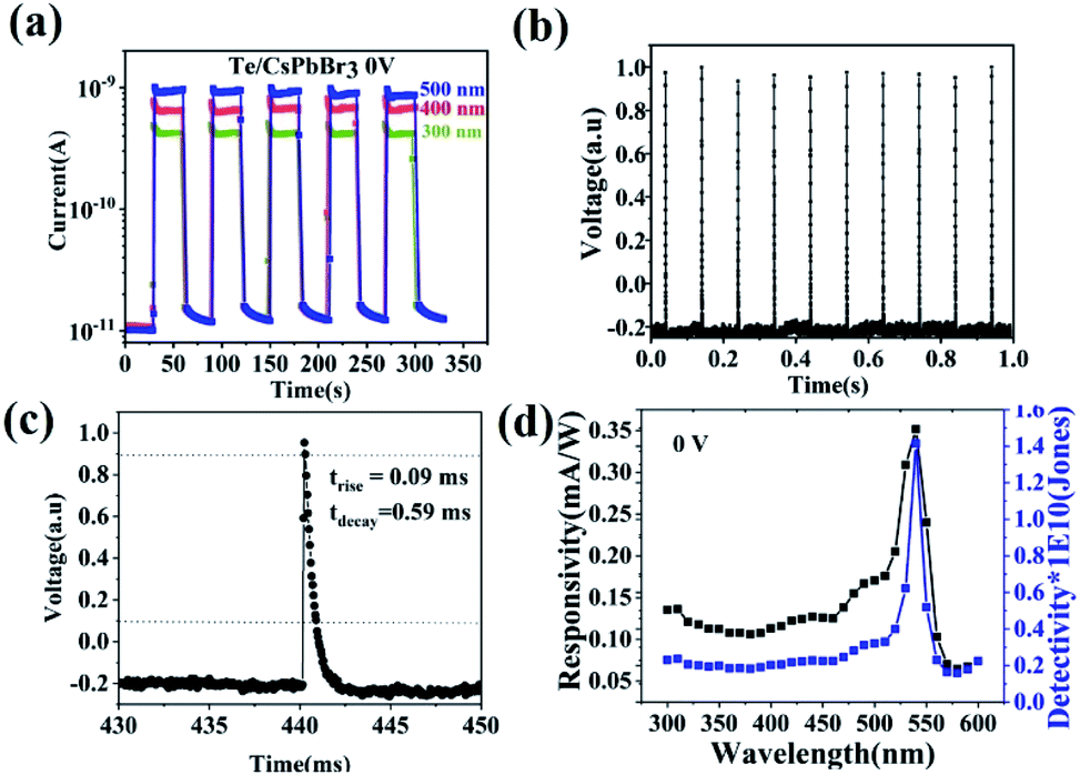 | ||
| Fig. 5 (a) I–t curves of the Te/CsPbBr3 PDs upon 500, 400, 300 nm illumination under biases of 0 V; (b) photoresponse of Te/CsPbBr3 PDs under 355 nm pulse laser radiation at zero bias; (c) single period of pulse response; (d) responsivity and detectivity of the Te/CsPbBr3 PDs at 0 V bias. | ||
Based on the Te wire, the heterojunction device formed by CsPbBr3 particles clearly shows an ultra-fast response speed. Spectral responsivity (Rλ) is another key factor for evaluating the characteristics of PDs, which was calculated according to the following formula:
 | (1) |
 | (2) |
To understand the self-powered mechanism of Te/CsPbBr3 PDs, Fig. 6a shows a schematic of the built-in electric field and energy level formed at the interface of p-Te and n-CsPbBr3. The simplified structure diagram of Te/CsPbBr3 PD is shown in Fig. 6b. The self-powered characteristics of the device are mainly due to the heterojunction formed at the interface between the p-type Te wire and the n-type CsPbBr3 particles.31,32 The CsPbBr3 particles were deposited on the surface of the Te wire, and the device exhibited a type-II heterojunction.32,33 The band gaps of Te and CsPbBr3 were 0.35 eV and 2.3 eV, respectively.34,35 Under light irradiation, the photogenerated electrons and holes were rapidly separated by the built-in field of the depleted layer. The photo-generated holes in the CsPbBr3 particles were transferred to the valence band of the Te semiconductor, and the electrons in the conduction band of the Te semiconductor drifted into CsPbBr3, thereby forming a photovoltage and a stable photocurrent at the interface.36,37 This device can be regarded as a Te/CsPbBr3 p–n heterojunction photodiode. Due to the excellent intrinsic physical properties of Te and CsPbBr3, the Te/CsPbBr3 heterojunction has a high photocurrent, fast response speed, and a high on/off ratio at 0 V. Due to the narrow Te band gap, the device can respond to ultraviolet and visible light. Therefore, the Te wire is the main carrier transport channel and provides the driving force for the built-in electric field.
 | ||
| Fig. 6 (a) Schematic energy-band diagrams of the Te/CsPbBr3 PDs; (b) simplified schematic of the Te/CsPbBr3 structure. | ||
4. Conclusion
The long Te wire was synthesized by chemical vapor deposition, where CsPbBr3 particles were formed on the Te wire surface and then heated to form the p–n heterojunction. CsPbBr3 particles were then deposited onto the surface of the Te wires and a built-in field formed between Te and CsPbBr3. This made the device self-powered and exhibits characteristics of broad-spectrum response (UV-visible) and ultra-fast response speed (trise = 0.09 ms). The open-circuit voltage of Te/CsPbBr3 PD was 0.5 V, which confirms the strong built-in electric field. In addition, under 0 V bias and upon 540 nm light irradiation, the devices had good responsivity (0.35 mA W−1), high photosensitivity (up to 100 on/off ratio), and detectivity of 1.42 × 10¹⁰ Jones per W. This study provides a simple and effective method for the in situ preparation of heterojunctions. All these promising characteristics show that the composite Te/CsPbBr3 device has a wide range of application prospects in the field of optoelectronic devices.Conflicts of interest
The authors declare no conflict of interest.Acknowledgements
This work was financially supported by the National Natural Science Foundation of China (Grant No. 11904034) and Natural Science Foundation of Jiangsu Province of China (Grant No. BK20191025). Zhang Jie acknowledged the support of the National Natural Science Foundation of China (Grant No. 61704012).References
- G. Pelayo, A. Armin, P. Meredith and E. H. Sargent, Nat. Rev. Mater., 2017, 2, 16100 CrossRef.
- M. Cao, W. Zhao, R. Li, H. Gong, Y. Zhang, H. Xu and J. R. Lu, ACS Appl. Mater. Interfaces, 2018, 10, 24937–24946 CrossRef CAS PubMed.
- X. Y. Zhao, L. X. Huang, Y. K. Wang, X. L. Zhu, L. Li, G. X. Li and W. H. Sun, RSC Adv., 2020, 10, 32976–32983 RSC.
- Z. B. He, J. X. Guo, S. D. Li, Z. C. Lei, L. Lin, Y. Z. Ke, W. J. Jie, T. X. Gong, Y. Lin, T. D. Cheng, W. Huang and X. S. Zhang, Adv. Mater. Interfaces, 2020, 7, 2070050 CrossRef.
- D. Periyanagounder, T. C. Wei, T. Y. Li, C. H. Lin and T. P. Goncalves, et al., Adv. Mater., 2020, 32, 1904634 CrossRef CAS PubMed.
- F. Teng, K. Hu, W. X. Ouyang and X. S. Fang, Adv. Mater., 2018, 30, 1706262 CrossRef PubMed.
- B. S. Ouyang, K. W. Zhang and Y. Yang, Adv. Mater. Technol., 2017, 2, 1700208 CrossRef.
- Y. Zhang and W. D. Song, J. Mater. Chem. C, 2021, 9, 4799–4807 RSC.
- Y. Zhang, W. L. Liu, Y. S. Liu, C. H. Wag, G. D. Zhu and W. D. Song, J. Mater. Chem. C, 2021, 9, 15654–15661 RSC.
- J. W. Liu, F. Chen, M. Zhang, H. Qi, C. L. Zhang and S. H. Yu, Langmuir, 2010, 26, 11372–11377 CrossRef CAS PubMed.
- J. Yuan, H. Schmalz, Y. Xu, N. Miyajima, M. Drechsler, M. W. Möller, F. Schacher and A. H. E. Müller, Adv. Mater., 2010, 20, 947–952 CrossRef.
- G. She, W. Shi, X. Zhang, T. Wong, Y. Cai and N. Wang, Cryst. Growth Des., 2013, 9, 663–666 CrossRef.
- Q. P. Zhang, M. M. Tavakoli, L. L. Gu, D. Q. Zhang, L. Tang, Y. Gao, J. Guo, Y. J. Lin, S. F. Leung, S. Poddar, Y. Fu and Z. Y. Fan, Nat. Commun., 2019, 10, 727 CrossRef PubMed.
- V. V. Belykh, D. R. Yakovlev, M. M. Glazov, P. S. Grigoryev, M. Hussain, J. Rautert, D. N. Dirin, M. V. Kovalenko and M. Bayer, Nat. Commun., 2019, 10, 673 CrossRef CAS PubMed.
- C. H. Lin, B. Cheng, T. Y. Li, J. R. D. Retamal, T. C. Wei, H. C. Fu, X. S. Fang and J. H. He, ACS Nano, 2019, 13, 1168–1176 CAS.
- F. Chen, C. X. Xu, Q. Y. Xu, Y. Z. Zhu, F. F. Qin, W. Zhang, Z. Zhu, W. Liu and Z. L. Shi, ACS Appl. Mater. Interfaces, 2018, 10, 25763–25769 CrossRef CAS PubMed.
- L. Dou, Y. M. Yang, J. B. You, Z. R. Hong, W. H. Chang, L. Gang and Y. Yang, Nat. Commun., 2014, 5, 5404 CrossRef CAS PubMed.
- Q. Q. Lin, A. Armin, D. M. Lyons, P. L. Burn and P. Meredith, Adv. Mater., 2015, 27, 2060–2064 CrossRef CAS PubMed.
- N. Yantara, S. Bhaumik, F. Yan, D. Sabba, H. A. Dewi, N. Mathews, P. P. Boix, H. V. Demir and S. Mhaisalkar, J. Phys. Chem. Lett., 2015, 6, 4360–4364 CrossRef CAS PubMed.
- L. Protesescu, S. Yakunin, M. I. Bodnarchuk, F. Krieg, R. Caputo, C. H. Hendon, R. X. Yang, A. Walsh and M. V. Kovalenko, Nano Lett., 2015, 15, 3692–3696 CrossRef CAS PubMed.
- Y. Zhang, S. Y. Li, W. Yang, M. K. Joshi and X. S. Fang, J. Phys. Chem. Lett., 2019, 10, 2400–2407 CrossRef CAS PubMed.
- Y. Zhang, W. X. Xu, X. J. Xu, J. Cai, W. Yang and X. S. Fang, J. Phys. Chem. Lett., 2019, 10, 836–841 CrossRef CAS PubMed.
- U. K. Gautam and C. N. R. Rao, J. Mater. Chem., 2004, 14, 2530–2535 RSC.
- J. Ding, S. Du, Z. Zuo, Y. Zhao, H. Cui and X. Zhan, J. Phys. Chem. C, 2017, 121, 4917–4923 CrossRef CAS.
- M. Shoaib, X. Zhang, X. Wang, H. Zhou, T. Xu, X. Wang, X. Hu, H. Liu, X. Fan and W. Zheng, et al., J. Am. Chem. Soc., 2017, 139, 15592–15595 CrossRef CAS PubMed.
- Y. Zhang, W. X. Xu, X. J. Xu, W. Yang, S. Y. Li, J. X. Chen and X. S. Fang, Nanoscale Horiz., 2019, 4, 452–456 RSC.
- Y. L. Shen, C. Wei, L. B. Ma, S. L. Wang, X. Wang, X. B. Xu and H. B. Zeng, J. Mater. Chem. C, 2018, 6, 12164–12169 RSC.
- H. J. Zhang, X. Liu, J. P. Dong, H. Yu, C. Zhou, B. B. Zhang, Y. D. Xu and W. Q. Jie, Cryst. Growth Des., 2017, 17, 6426–6431 CrossRef CAS.
- Z. Yang, Q. Xu, X. D. Wang, J. F. Lu, H. Wang, F. T. Li, L. Zhang, G. F. Hu and C. F. Pan, Adv. Mater., 2018, 30, 1802110 CrossRef PubMed.
- B. Zhao, F. Wang, H. Y. Chen, Y. P. Wang, M. M. Jiang, X. S. Fang and D. X. Zhao, Nano Lett., 2015, 15, 3988–3993 CrossRef CAS PubMed.
- S. Liang, Y. Fang, H. Wei, Y. Yuan and J. Huang, Adv. Mater., 2016, 28, 2043–2048 CrossRef PubMed.
- W. X. Ouyang, F. Teng and X. S. Fang, Adv. Funct. Mater., 2018, 28, 1707178 CrossRef.
- W. X. Ouyang, F. Teng, J. H. He and X. S. Fang, Adv. Funct. Mater., 2019, 29, 1807672 CrossRef.
- H. H. Li, P. Zhang, C. L. Liang, J. Yang, M. Zhou, X. H. Lu and G. A. Hope, Cryst. Res. Technol., 2012, 47, 1069–1074 CrossRef CAS.
- X. Y. Liu, X. H. Tan, Z. Y. Liu, X. N. Zhang, T. L. Shi and G. L. Liao, J. Mater. Chem. C, 2020, 8, 14409–14422 RSC.
- N. Gao and X. S. Fang, Chem. Rev., 2015, 115, 8294–8343 CrossRef CAS PubMed.
- A. Alarawi, V. Ramalingam, H. C. Fu, P. Varadhan, R. S. Yang and J. H. He, Opt. Express, 2019, 27, A352–A362 CrossRef CAS PubMed.
| This journal is © The Royal Society of Chemistry 2022 |