DOI:
10.1039/D1RA08103A
(Paper)
RSC Adv., 2022,
12, 11649-11656
Improved resistive switching characteristics of a multi-stacked HfO2/Al2O3/HfO2 RRAM structure for neuromorphic and synaptic applications: experimental and computational study†
Received
4th November 2021
, Accepted 3rd April 2022
First published on 14th April 2022
Abstract
Atomic Layer Deposition (ALD) was used for a tri-layer structure (HfO2/Al2O3/HfO2) at low temperature over an Indium Tin Oxide (ITO) transparent electrode. First, the microstructure of the fabricated TaN/HfO2/Al2O3/HfO2/ITO RRAM device was examined by the cross-sectional High-Resolution Transmission Electron Microscopy (HRTEM). Then, Energy Dispersive X-ray Spectroscopy (EDS) was performed to probe compositional mapping. The bipolar resistive switching mode of the device was confirmed through SET/RESET characteristic plots for 100 cycles as a function of applied biasing voltage. An endurance test was performed for 100 DC switching cycles @0.2 V wherein; data retention was found up to 104 s. Moreover, for better insight into the charge conduction mechanism in tri-layer HfO2/Al2O3/HfO2, based on oxygen vacancies (VOX), total density of states (TDOS), partial density of states (PDOS) and isosurface three-dimensional charge density analysis was performed using WEIN2k and VASP simulation packages under Perdew–Burke–Ernzerhof _Generalized Gradient approximation (PBE-GGA). The experimental and theoretical outcomes can help in finding proper stacking of the active resistive switching (RS) layer for resistive random-access memory (RRAM) applications.
1. Background
In the era of next-generation non-volatile storage devices, resistive random-access memory devices have attracted the attention of scientists. RRAM has become a promising storage device due to its simple metal–semiconductor–metal physical morphology,1 fast switching speed, low power consumption, long data retention, and improved endurance. The simplest structure metal–insulator–metal (MIM) of RRAM devices leads to easy fabrication into a passive crossbar array even with nano size.2,3 The key factors influencing device performance are choice of electrode material4,5 and resistive switching (RS) active oxide layer.6–9 Conventionally, the top electrode is an active metal like Ag,10 Cu11 and Ni12 etc. While the bottom electrode is made up of an inert (non-reactive) metal like Pt, Pd etc.13 In the resistive switching devices, in the case of electrochemical metallization mechanism (ECM), electrochemically active metals such as Cu, Ag etc. Become oxidized depending on the electric field during electroforming as oxygen ions drift toward the active electrode leaving vacancies behind. On the other hand, inert (non-reactive) electrode contributes to the electrical charge transport without any noticeable oxidation and has very insignificant role in resistive switching performance.14,15
Most conventional dielectric metal oxides have been used so far for RS (Resistive Switching) active layer like Al2O3,16 HfO2,17,18 SiO2,19 Nb2O5,20 TiO2(ref. 21) and WO3(ref. 22) etc. Due to simple composition, RRAM devices with transition metal oxides as active RS layer have been widely explored. However, non-uniformity of switching states of transition metal oxide-based cells limits its operation.
The phenomenon of resistive switching is based on formation and rupture of conducting filaments (CFs)23 generated as a result of the movement of oxygen atoms towards electrode leaving behind oxygen vacancies (VOX) within the active RS layer. This movement of oxygen atoms and formation of oxygen vacancies (VOX) effectively alters the resistance state of the RS layer between two electrodes, ultimately changing the morphology of interfacial charge barrier.24 The presence of oxygen vacancy and dopants causes clustering of more oxygen vacancies in localized states, which give rise to the formation of conducting filaments.25 The monolayer (Al2O3) based RRAM devices have been reported to have random and uncontrolled formation of conducting filaments with larger biasing voltage.26–28 So, the research community has focused on synthesizing bi-layer and tri-layer RRAM devices to cope with the randomness of formation of CFs. In recent years most prominent bi-layer type RRAM structures found are HfO2/TiOx, Al2O3/TiO2, Al2O3/Ta2O5, HfOx/HfO2 and TaOx/Al2O3 etc.29–32 In these bi-layer type RRAM devices, usually oxygen vacancies have been reported at the interface of two layers where formation of oxygen vacancies due to movement of O-atoms towards respective electrode causes variation in switching states i.e., from low resistance state (LRS) to high resistance state (HRS) and vice versa.33 This movement of O-atoms and formation of VOX between two layers also limit the magnitude of current needed for switching and power consumption in RRAM devices. Al2O3/HfO2/Al2O3 has been discussed by Wang et al. with surprising switching performance.34 In their study, Wang and his co-authors found a high concentration of oxygen vacancies in HfO2 compared to the Al2O3 layer, which leads to the migration of those oxygen vacancies from layer richer in VOX towards layer deficient in VOX. Quite coherent study has been also presented by Lui et al. for Al2O3/HfO2/Al2O3 type RRAM device.35
In the present study, we have an experimental and computational insight of the tri-layer structure of RRAM with Al2O3 as a middle layer packed between two layers of HfO2.In experimental section, vacancies are usually introduced during synthesis of thin layered structures as no structure obtained experimentally is a perfect one. In addition, when positive biasing electric field is applied to the top electrode keeping bottom electrode ground, oxygen ions are extracted from the adjacent oxide layer, which drift toward top electrode leaving oxygen vacancies behind. These oxygen vacancies are capable of arranging themselves in line pattern, and hence generate conductive filaments between top and bottom electrodes. That is why, conduction phenomenon observed in the studied layer structure is expected to be due to these oxygen vacancies. Many researchers have reported earlier occurrence of Vox in Al2O3 layers.33–35 In this study, therefore, we have focused on theoretical confirmation about the role of Vox in Al2O3 and HfO2 structure. For this purpose, Vox are introduced in Al2O3 layer near the Al2O3/HfO2 interface. It is anticipated that present study will provide scientists suitable morphology about stacking scheme of RS active layer for RRAM applications.
2. Layer preparation and computational details
2.1 Experimental details
Initially, the bottom electrode was taken as commercially available ∼40 nm-thick Indium Tin Oxide (ITO)(sheet resistance of ∼60 Ω sq−1) on SiO2 glass. Sequential ITO surface cleaning procedure was adopted stepwise with acetone, isopropyl alcohol, and deionized water along with ultrasonication for 5 min. Finally, it was dried using an N2 blow at room temperature. Cleaned ITO substrates were immediately transferred to the Atomic Layer Deposition (ALD) system for Al2O3 and HfO2 deposition at low substrate temperature. Tri-layer of HfO2 (5.5 nm)/Al2O3 (1 nm)/HfO2 (5.5 nm) was deposited by using the metal precursors of Tetrakis (ethylmethylamino) hafnium (TEMAH) and trimethylaluminum (TMA) for HfO2 and Al2O3 respectively. In this ALD technique, H2O was used as the oxidant at a substrate temperature of 150 °C. Sputtered TaN was used as a top electrode with Ni capping layer and electrodes were formed by the liftoff process to achieve an area of 100 × 100 μm2. Fig. 1 shows the schematics of the fabricated tri-layer RRAM device. For electrical resistive switching (I–V) and pulse measurements to characterize synaptic properties of the fabricated device, Keithley 4200 SCS semiconductor parameter analyzer, and 4225-PMU ultrafast current–voltage (I–V) pulse module were used. All electrical measurements were done by applying a voltage to the top TaN electrode while the ITO bottom electrode (BE) was grounded.
 |
| | Fig. 1 Schematic of Ni/TaN/HfO2/Al2O3/HfO2/ITO RRAM device structure with TaN top and ITO bottom electrodes. | |
2.2 Theoretical details
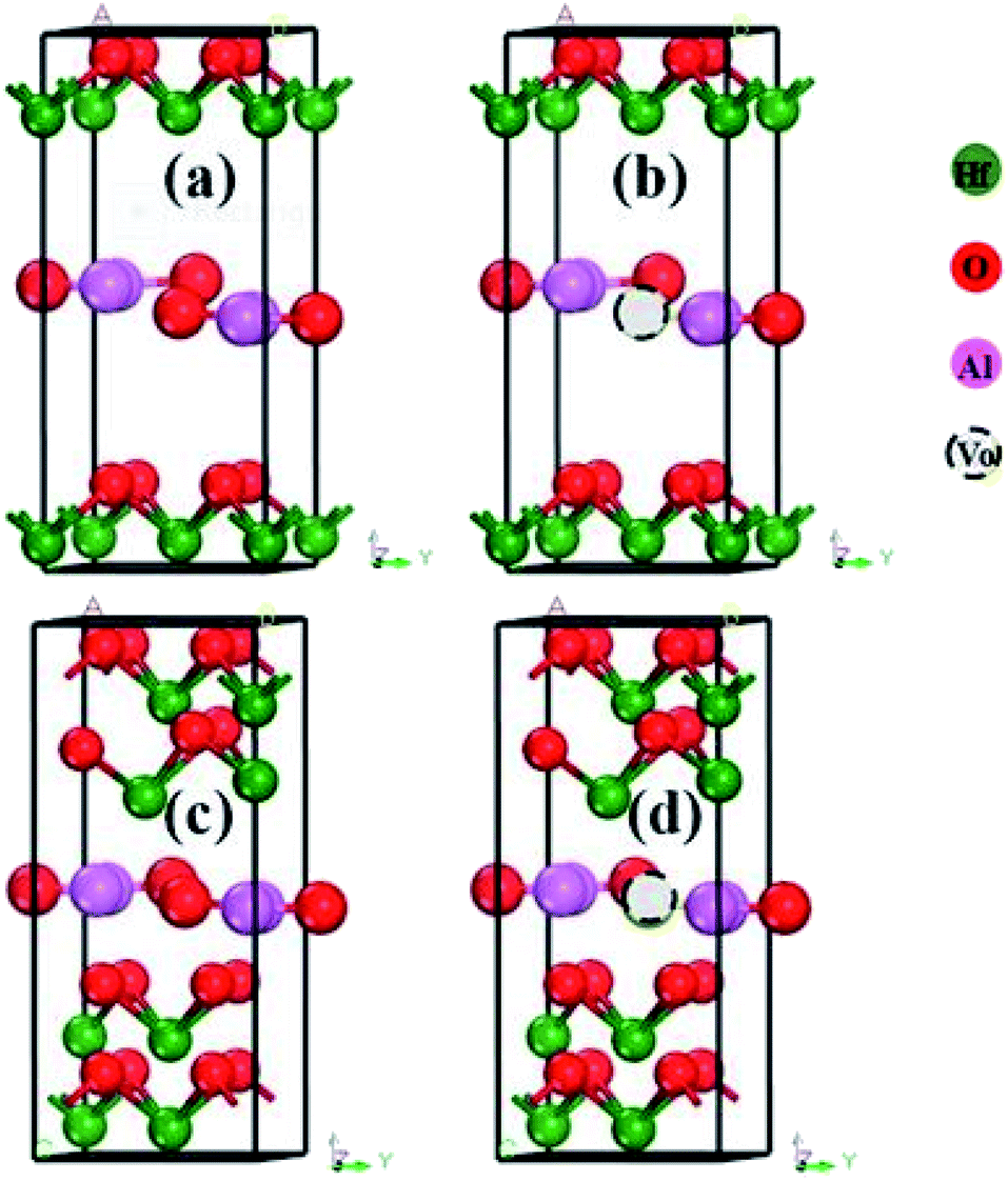
In addition, for theoretical analysis of charge conduction mechanism using DOS and isosurface charge density results, calculations were performed within the frame work of WEIN2k simulation package36 and Vienna ab initio simulation package (VASP)36,37 under Perdew–Burke–Ernzerhof Generalized Gradient Approximation (PBE-GGA) method to solve Kohn Sham DFT equations.38 Amongst various exchange correlation functional, PBE-GGA is most convenient for semiconductor systems. Moreover, it is a non-empirical functional with better accuracy and low computational cost for various systems.36,38 The energy convergence test was performed using K-points sampling where convergence was found within 0.1 meV for both codes (WEIN2k, VASP) and cutoff energy was chosen to be 480 eV with 1000 K-points. In order to get the energy eigenvalue convergence, the cutoff planewave parameter was selected as KmaxxRMT = 7.5 and Gaussian parameter (Gmax) was taken as 14Ry1/2. In order to have low computational cost, thin tri-layer (HfO2/Al2O3/HfO2) was modeled holding supercell of 42 and 41 atoms with HfO2 (17-atoms/top and bottom layer) and Al2O3 (08/07-atoms) without and with VOX respectively. Whereas, bi-stacked-layer (HfO2–HfO2/Al2O3/HfO2–HfO2) without and with VOX was opted with supercell containing 76- and 75-atoms respectively including 08/07-atoms of Al2O3 and 17-atoms for each HfO2 layer. Experimentally, oxygen vacancies are automatically introduced during thin layer structure preparation and during electroforming process. While, theoretically we have introduced VOX at the Al2O3/HfO2 interface. Fig. 2 shows the basic modeled layer structure and geometry optimization plots are shown in Fig. S1.† It has been reported earlier by Umberto et al. that choice of thin layer oxide causes controlled interfacial drifting of O-atoms and appearance of VOX.39
 |
| | Fig. 2 The modeled structures of (a) HfO2/Al2O3/HfO2 (b) HfO2/Al2O3 + Vox/HfO2 (c) HfO2–HfO2/Al2O3/HfO2–HfO2 and (d) HfO2–HfO2/Al2O3 + Vox/HfO2–HfO2. | |
3. Results and discussion
3.1 Experimental results
Fig. 3 shows the nanostructure of fabricated TaN/HfO2/Al2O3/HfO2/ITO RRAM device examined by the cross-sectional High-Resolution Transmission Electron Microscope (HRTEM). This microscopic image confirms the total thickness of tri-layer ∼12 nm coherent with the target thickness. For further confirmation of tri-layer structure HfO2/Al2O3/HfO2, Energy Dispersive X-ray Spectroscopy (EDS) was performed to justify the elemental composition mapping with different colors, as shown in Fig. 4. The EDS results confirm the tri-layer structure HfO2/Al2O3/HfO2 without any significant diffusion of any other element. Also, the presence of humps depicts the interface-diffusion between HfO2/Al2O3. During thin film synthesis, oxygen vacancies are formed, also during electroforming process vacancies are also created due to applied biasing field. These Vox arrange themselves in line pattern to form conduction filaments. A similar finding has been described from isosurface charge density with charge depletion and accumulation at the layer interface as discussed in a later section.
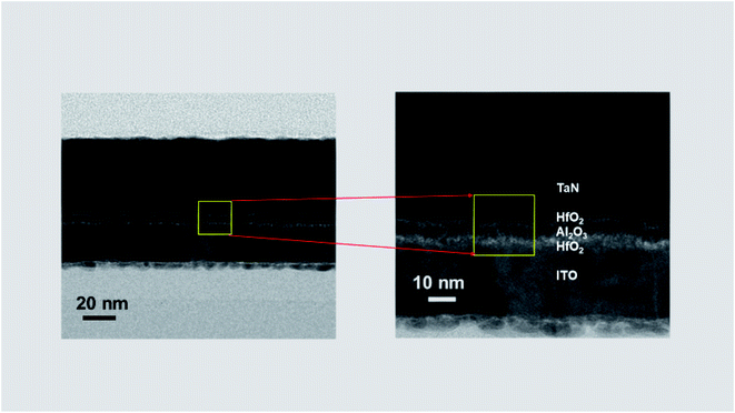 |
| | Fig. 3 Cross-sectional HRTEM images of tri-layer TaN/HfO2/Al2O3/HfO2/ITO RRAM structure. Clear individual layers are magnified on right side. | |
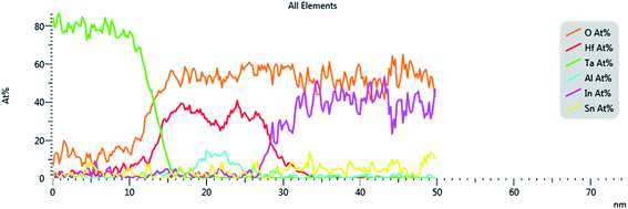 |
| | Fig. 4 EDS atomic percentage line profiles of Ta, Hf, Al, O, In, and Sn for the cross-section of the device. | |
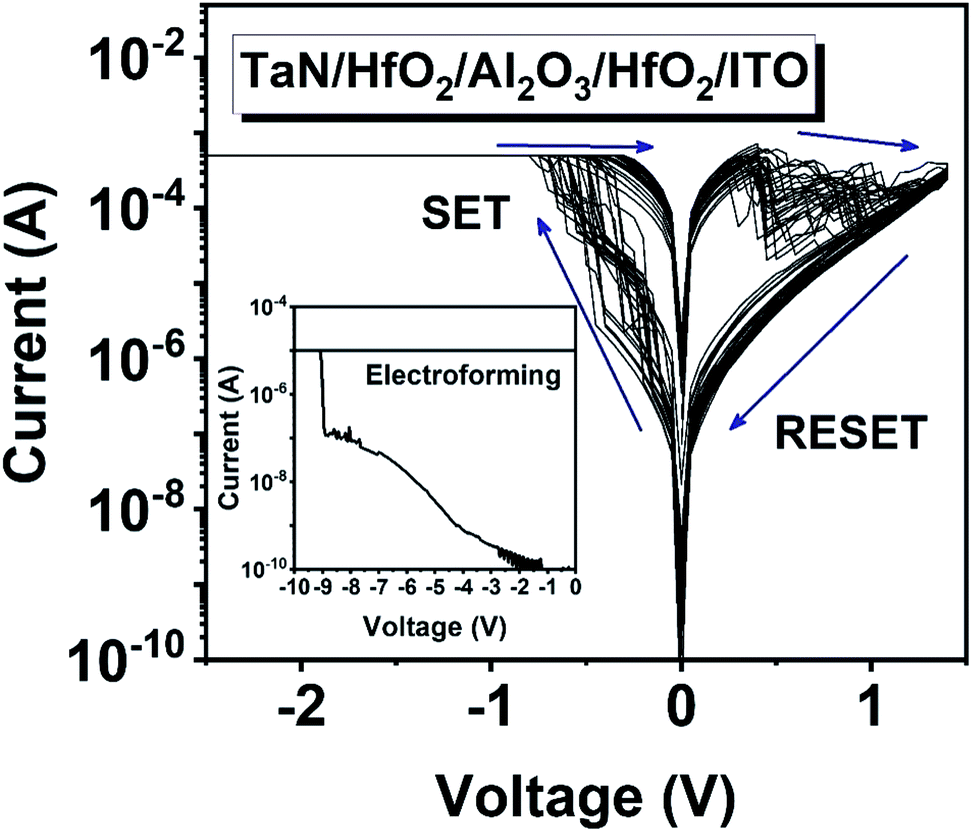
Fig. 5 displays the SET and RESET characteristics for up to 100 cycles of TaN/HfO2/Al2O3/HfO2/ITO tri-layer RRAM device. The current vs. voltage (I–V) plot shows bipolar resistive switching wherein opposite polarity is needed at the top electrode for SET and RESET processes.40 It is obvious from I–V plot that first RESET exhibits a larger current than other repeated cycles, which might be a consequence of the discharging effect of parasitic capacitance through the CFs.14 During RESET process the application of opposite polarity biasing to top electrode causes the rupturing of CFs that may be result of recombination of oxygen vacancies and oxygen ions. In case of tri-layer structure (HfO2/Al2O3/HfO2) as in present study, the rupturing of CFs takes place at Al2O3/HfO2 interface only and even after RESET process entire filament is not ruptured. This enhances the switching characteristics for multi-layer structure as presented earlier by Zhang et al.41 During electroforming process, the 10−5. A current compliance (Icc) was opted to prevent the device switching failure in line with literature.42,43 It has been earlier reported that during electroforming process the oxygen vacancies shift towards the ITO electrode and create CFs while, oxygen anions drift toward opposite (Top) electrode.41,44 For better insight of shifting of VOX, theoretical calculations have been performed wherein defect states (green highlighted states) are found near the Fermi level inside Valence Band (V.B), crossing Fermi level and extending deep inside the Conduction Band (C.B) region of Total Density of States (TDOS). Such states might result from interfacial charge exchange between layers as discussed in later theoretical section. Moreover, charge diffusion and formation of CFs during the electroforming process has been calculated using three-dimensional isosurface charge density in theoretical section.
 |
| | Fig. 5 Consecutive 100 SET/RESET bipolar resistive switching cycles of Ni/TaN/HfO2/Al2O3/HfO2/ITO tri-layer RRAM device. Inset shows the electroforming characteristics. | |
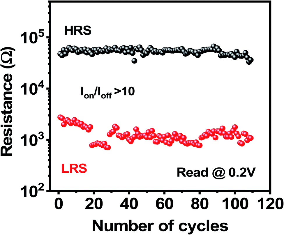
The endurance characteristics for tri-layer RRAM device for 100 switching cycles at read voltage value of 0.2 V has been performed as shown in Fig. 6. The HRS value is constant for 100 cycles, which refers to the stability of resistive switching corresponding to the resistance between 10–100 kΩ. It is worth noticing that decay in resistance is due to the deposition of oxygen ions near the electrode during RESET process, which reflects insufficient recombination of oxygen vacancies.45 This effect has been endorsed by the charge depletion pattern about oxygen atoms as displayed in the computational section in isosurface charge density plots. The gradual decrease in Low Resistance State (LRS) after initial cycles indicates broadening of the width of CFs during RS mechanism.46
 |
| | Fig. 6 Endurance characteristics of tri-layer RRAM device for 100 switching cycles at a read voltage of 0.2 V. | |
Fig. 7 presents the memory retention properties of HRS and LRS for retention time of 104 s at read voltage of 0.2 V for RRAM device. It is worth noticing that HRS/LRS remains constant without any degradation for a time of 104 s, which suggests the device's reliability with controlled conduction filament formation. The controlled CFs formation shows the uniform distribution of oxygen vacancies and satisfactory data retention comparable to the available literature.47 It is also noted that the HRS values in Fig. 7 are lower than those in Fig. 6. Such types of variations have been noticed in many RRAM devices such as Pt/Ti/CeO2/Al/CeO2/Pt48 and particularly in devices with TaN as top electrode like TaN/CeO2/Al/CeO2/Pt49 and TaN/CeO2/Ti/CeO2/Pt50 devices. Such behavior causes variations in HRS/LRS ratio from device to device. Device to device HRS/LRS ratio might also vary due to the large area of RRAM device (i.e., 100 × 100 μm2). During electroforming process, either single or multiple conductive filaments are formed between top and bottom electrodes. In the SET and RESET processes of resistive switching, these filaments play vital role causing rise or fall of resistance in the low and/or high resistance states. Such device-to-device variation can be controlled by reducing the top electrode area.
 |
| | Fig. 7 Memory retention characteristics of HRS and LRS for 104 s with a read voltage of 0.2 V for RRAM device. | |
3.2 Computational results
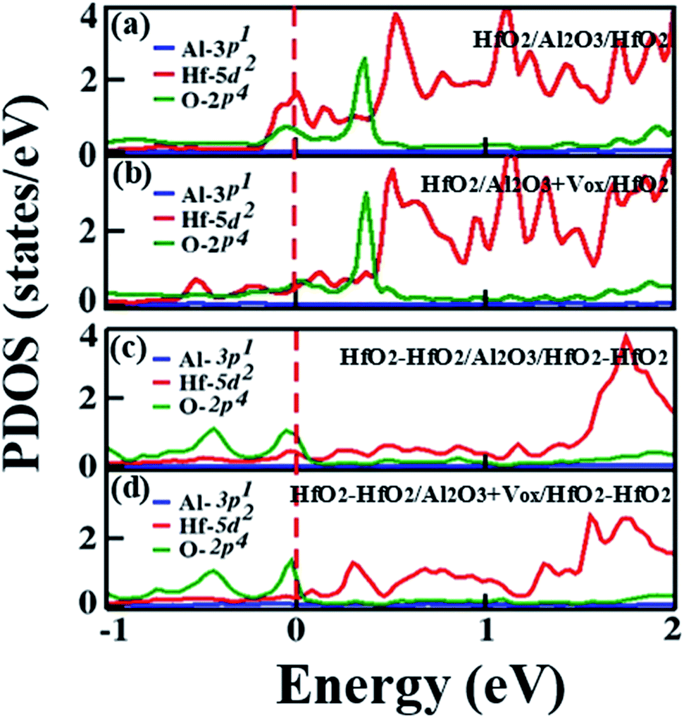
3.2.1 Total and partial density of states. For better understanding of the charge conduction phenomenon and formation of CFs, total density of states (TDOS), partial density of states (PDOS) and three dimensional isosurface charge density calculations have been performed using PBE-GGA approach. The TDOS findings using VASP package are shown in Fig. S2 in ESI† where less energy states are found. Effect of Vox on conductivity is clear from changing number of localized states in V.B and C.B. We have also performed TDOS and PDOS calculations under framework of WEIN2k code for better insight of defect states. Fig. 8(a and b) depicts the TDOS results for tri-layer (HfO2/Al2O3/HfO2) without and with VOX. In the presence of VOX, some extra defect states (highlighted in green) are found in V.B and C.B, while shifting of energy states across the Fermi level endorse the interfacial charge diffusion as predicted in experimental findings. It has been suggested earlier that the occurrence of VOX paves the charge conduction path at the interface of two dielectric layers.46 Moreover, diffusion of charges (oxygen ions) at the interface causes electrical link (CFs) between top and bottom electrodes and device shifts to low resistance state (ON-state).46 A continuous variation in switching states makes the device suitable also for future synaptic and neuromorphic applications.51 Additionally, to check effect of thickness of the RS active layer, we have theoretically studied electronic characteristics of bi-stacked tri-layer i.e., HfO2–HfO2/Al2O3/HfO2–HfO2. For bi-stacked tri-layer i.e., HfO2–HfO2/Al2O3/HfO2–HfO2 less localized energy states are found above the Fermi level in V.B and C.B as shown in Fig. 8(c). However, the presence of VOX within this bi-stacked tri-layer (as depicted in Fig. 8(d)) gives defect energy states deep inside the C.B far from the Fermi level, which might be a consequence of presence of more dielectric interfaces where bi-stacking of HfO2 extracts more available VOX causing non-uniformity of charge conduction. Henceforth bi-stacked tri-layer (HfO2–HfO2/Al2O3/HfO2–HfO2) is not suitable for fabrication of compatible RRAM devices.
 |
| | Fig. 8 Calculated TDOS results without/with VOX for (a)tri-layer HfO2/Al2O3/HfO2 and (b) bi-stacked tri-layer HfO2–HfO2/Al2O3/HfO2–HfO2 RRAM device where green highlighted ovals show defect states consequence of recombination of VOX. | |
The partial density of states (PDOS) results for tri-layer device without Vox as shown in Fig. 9(a) elaborate that valence band and conduction band formation is a consequence of hybridization of Hf-5d and O-2p states. In the presence of VOX, as displayed in Fig. 9(b), this hybridization seems to be stronger because of extra available defect states as found in TDOS results. The presence of these defect states in V.B and C.B regions results from contribution of Hf-5d and O-2p electrons. This gives rise to interfacial diffusion of Vox across the layers. These findings unveil the fact that introducing VOX at the layer interface assists in shifting of energy states across the Fermi level and some defect states appear in V.B and C.B as well. This might be a consequence of diffusion of VOX into Hf-oxide layer where VOX concentration gets multiplied and ultimately controls switching phenomenon. In case of bi-stacked tri-layer i.e., HfO2–HfO2/Al2O3/HfO2–HfO2 without and with VOX, there seems major involvement of Hf and O atoms with least contribution of Al-atoms in the formation of V.B and C.B as represented in Fig. 9(c and d). However, here the energy states of elements are found with less sharp peaks leading to minimal charge conduction regions consistent with TDOS results.
 |
| | Fig. 9 The calculated PDOS results without/with VOX for (a) tri-layer HfO2/Al2O3/HfO2 and (b) bi-stacked tri-layer HfO2–HfO2/Al2O3/HfO2–HfO2 RRAM device. | |
3.2.2 Iso-surface charge density. For better understanding of charge conduction mechanism, we have calculated three dimensional isosurface charge density using VASP code.37 The iso-surface charge density scheme for tri-layer system (HfO2/Al2O3/HfO2), where charge accumulation is represented by yellow color near (Hf atoms) while cyan color show charge depletion around the atom (oxygen atoms). It has been observed that Hf-atoms (colored green) accumulate the charges and charge depletion appears about oxygen atoms (red colored atoms). The accumulation and depletion of charges at the interface of (HfO2/Al2O3/HfO2) give rise to an electrical link between bottom HfO2 and central Al2O3 layer, leading to the formation of CFs. Here CFs grows along positive c-direction of three-dimensional symmetry. The formation of CFs plays pivotal role in changing the switching state of devices i.e., it transforms the device from HRS to LRS.46,47 It has been reported earlier that VOX shifting occurs between layer rich in oxygen and region with minimal oxygen atoms52–54 in line with our theoretical finding. In the present study, VOX diffusion from Al2O3 is found towards HfO2 coherent with the previous study.55 The interfacial diffusion of VOX between Al2O3 and HfO2 is suspected to generate essential vacancy trap sites that further control the switching mechanism in accordance with literature.56 Also, formation of CFs along a particular dimension gives constant HRS/LRS which ensures the data retention of the device as observed from experimental findings, as shown in Fig. 7. The integrated charge density quantitatively calculates charge depletion and accumulation as shown in Fig. 10(b) which better estimates the size of CFs. The overall performance of RRAM and synaptic devices is based on physical morphology/size of CFs.34 Fig. 11(a and b) indicates the isosurface three-dimensional and integrated charge density for bi-stacked tri-layer (HfO2–HfO2/Al2O3/HfO2–HfO2). In this case minimal charge depletion and accumulation takes place so no symmetric CFs have been observed. Also, such type of multilayer structure causes diffusion of VOX and acceptance of O-ions between Hf-oxide layers that behave as virtual electrodes57 without generating any electrical link to top/bottom electrode. In both cases, no interfacial charge diffusion takes place in the region between two blue dashed lines consistent with qualitative isosurface charge density. This is due to formation of CFs from one interface making this side active for connecting active electrode. It is worth noting that CFs are formed where Vox are introduced theoretically (Fig. 2). Whereas, CFs will extend through other interface when biased as explained by bipolar switching in experimental section. This theoretical finding could assist the scientists to better estimate the thickness of active metal oxide layer while synthesizing RRAM devices for neuromorphic applications.
 |
| | Fig. 10 For HfO2/Al2O3/HfO2 device, calculated (a) three-dimensional isosurface charge density plot, in which depletion and accumulation of charges is represented by cyan and yellow colors respectively. Green, purple and red balls indicate Hf, Al and O atoms respectively. (b) Integrated charge density verse distance plot. Rectangular highlighted light blue and purple colors represent HfO2 and Al2O3 layers. Whereas, light green oval shape is indicating interfacial effect between HfO2 and Al2O3. | |
 |
| | Fig. 11 For bi-stacked HfO2–HfO2/Al2O3/HfO2–HfO2 device, calculated (a) three-dimensional isosurface charge density plot, where depletion and accumulation of charges is represented by cyan and yellow colors respectively. Green, purple and red balls indicate Hf, Al and O atoms respectively. (b) Integrated charge density verses distance plot. Rectangular highlighted light blue and purple colors are representing HfO2 and Al2O3 layers. | |
4. Summary
In the present work, tri-layer (HfO2/Al2O3/HfO2) is fabricated using atomic layer deposition technique and bipolar switching has been reported using I–V characteristics curves. The endurance test has been performed for 100 switching cycles at read voltage value of 0.2 V and at the 42nd cycle value fluctuation is found a little bit corresponding to the resistance between 10–100 kΩ. The gradual decrease in low resistance state after initial cycles indicates the broadening of width of CFs during RS mechanism. It is worth noticing, HRS/LRS remains constant without any degradation for the time 104 s, which suggests the device's reliability with controlled conduction filament formation. Theoretical findings like TDOS and isosurface charge density clearly report the formation of CFs assisted by interfacial diffusion of charges and availability of VOX. Moreover, it has been found that the tri-layer (HfO2/Al2O3/HfO2) structure is most suitable compared to the bi-stacked tri-layer (HfO2–HfO2/Al2O3/HfO2–HfO2) configuration. The aforementioned results are suspected to be a source of motivation for scientists to fabricate and better analyze the stack thickness of active layer for RRAM/synaptic and neuromorphic applications.
Conflicts of interest
There are no conflicts to declare.
References
- E. A. Khera, H. Ullah, M. Imran, R. A. Khalil, F. Hussain and H. Algadi, Adv. Theory Simul., 2021, 4, 2100011 CrossRef CAS.
- X. Hong, D. J. Loy, P. A. Dananjaya, F. Tan, C. Ng and W. Lew, J. Mater. Sci., 2018, 53, 8720–8746 CrossRef CAS.
- O. Zakaria, M. Madi and S. Kasugai, J. Biomed. Mater. Res. B, 2020, 108, 460–467 CrossRef CAS PubMed.
- B. Khorolsuren, S. Lu, C. Sun, F. Jin, W. Mo, J. Song and K. Dong, J. Nanosci. Nanotechnol., 2020, 20, 6489–6494 CrossRef CAS PubMed.
- L. Sun, S. Dhale, S. Nalakath, M. Mohamadian, D. Luedtke, M. Preindl and A. Emadi, IEEE Transp. Electrif. Conf. Expo, 2019, 1–7 Search PubMed.
- Y. Wu, S. Yu, B. Lee and P. Wong, J. Appl. Phys., 2011, 110, 094104 CrossRef.
- N. Sedghi, H. Li, I. F. Brunell, K. Dawson, Y. Guo, R. J. Potter, J. T. Gibbon, V. R. Dhanak, W. D. Zhang, J. F. Zhang and S. Hall, Appl. Phys. Lett., 2017, 111, 092904 CrossRef.
- G. Zhou, Z. Ren, B. Sun, J. Wu, Z. Zou, S. Zheng, L. Wang, S. Duan and Q. Song, Nano Energy, 2020, 68, 104386 CrossRef CAS.
- G. Zhou, B. Sun, Z. Ren, L. Wang, C. Xu, B. Wu, P. Li, Y. Yao and S. Duan, Chem. Commun., 2019, 55, 9915–9918 RSC.
- D. Liang, X. Li, J. Wang, L. Wu and P. Chen, Solid-State Electron., 2018, 145, 46–48 CrossRef CAS.
- Y. Wang, H. Liu, X. Wang and L. Zhao, Nanoscale Res. Lett., 2019, 14, 1–9 CrossRef PubMed.
- Z. Shen, Y. Qi, I. Z. Mitrovic, C. Zhao, S. Hall, L. Yang, T. Luo, Y. Huang and C. Zhao, Micromachines, 2019, 10, 446 CrossRef PubMed.
- G. Wang, L. Hu, Y. Xia, Q. Li and Q. Xu, J. Magn. Magn. Mater., 2020, 493, 165728 CrossRef CAS.
- T. Shi, R. Wang, Z. Wu, Y. Sun, J. An and Q. Liu, Small Struct., 2021, 2, 2000109 CrossRef.
- Z. Shen, C. Zhao, Y. Qi, W. Xu, Y. Liu, I. Z. Mitrovic, L. Yang and C. Zhao, NanoMater, 2020, 10, 1437 CrossRef CAS PubMed.
- L. Chen, Y. Xu, Q. Q. Sun, H. Liu, J. J. Gu, S. J. Ding and D. W. Zhang, IEEE Electron Device Lett., 2010, 31, 356–358 CAS.
- Y. S. Chen, H. Y. Lee, P. S. Chen, C. H. Tsai, P. Y. Gu, T. Y. Wu, K. H. Tsai, S. S. Sheu, W. P. Lin, C. H. Lin and P. F. Chiu, Int. Electron Devices Meet., 2011, 31–33 Search PubMed.
- C. Walczyk, C. Wenger, R. Sohal, M. Lukosius, A. Fox, J. Dąbrowski, D. Wolansky, B. Tillack, H. J. Müssig and T. Schroeder, J. Appl. Phys., 2009, 105, 114103 CrossRef.
- C. Schindler, M. Weides, M. N. Kozicki and R. Waser, Appl. Phys. Lett., 2008, 92, 122910 CrossRef.
- H. Sim, D. Choi, D. Lee, S. Seo, M. J. Lee, I. K. Yoo and H. Hwang, IEEE Electron Device Lett., 2005, 26, 292–294 CAS.
- M. Fujimoto, H. Koyama, Y. Hosoi, K. Ishihara and S. Kobayashi, Jpn. J. Appl. Phys., 2006, 45, 310 CrossRef.
- M. N. Kozicki, C. Gopalan, M. Balakrishnan and M. Mitkova, IEEE Trans. Nanotechnol., 2006, 5, 535–544 Search PubMed.
- K. Fujiwara, T. Nemoto, M. J. Rozenberg, Y. Nakamura and H. Takagi, Jpn. J. Appl. Phys., 2008, 47, 6266 CrossRef CAS.
- J. J. Yang, M. D. Pickett, X. Li, D. A. Ohlberg, D. R. Stewart and R. S. Williams, Nat. Nanotechnol., 2008, 3, 429–433 CrossRef CAS PubMed.
- E. A. Khera, H. Ullah, M. Imran, N. A. Niaz, F. Hussain, R. A. Khalil, U. Resheed, A. M. Rana, M. I. Hussain, C. Mahata and S. Kim, J. Mol. Graph. Model., 2021, 103, 107825 CrossRef CAS PubMed.
- D. Conti, M. Laurenti, S. Porro, C. Giovinazzo, S. Bianco, V. Fra, A. Chiolerio, C. F. Pirri, G. Milano and C. Ricciardi, Nanotechnol, 2018, 30, 065707 CrossRef PubMed.
- J. Woo, K. Moon, J. Song, M. Kwak, J. Park and H. Hwang, IEEE Trans. Electron Devices, 2016, 63, 5064–5067 CAS.
- P. Parreira, G. W. Paterson, S. McVitie and D. A. MacLaren, J. Appl. Phys. D, 2016, 49, 095111 CrossRef.
- T. Tan, Y. Du, A. Cao, Y. Sun, H. Zhang and G. Zha, RSC Adv., 2018, 8, 41884–41891 RSC.
- R. Wang, T. Shi, X. Zhang, W. Wang, J. Wei, J. Lu, X. Zhao, Z. Wu, R. Cao, S. Long and Q. Liu, Materials, 2018, 11, 2102 CrossRef PubMed.
- W. Song, W. Wang, H. K. Lee, M. Li, V. Y. Q. Zhuo, Z. Chen, K. J. Chui, J. C. Liu, I. T. Wang, Y. Zhu and N. Singh, Appl. Phys. Lett., 2019, 115, 133501 CrossRef.
- H. Jeon, J. Park, W. Jang, H. Kim, S. Ahn, K. J. Jeon, H. Seo and H. Jeon, Carbon, 2014, 75, 209–216 CrossRef CAS.
- C. Mahata, M. Kang and S. Kim, Nanomater, 2020, 10, 2069 CrossRef CAS PubMed.
- L. G. Wang, X. Qian, Y. Q. Cao, Z. Y. Cao, G. Y. Fang, A. D. Li and D. Wu, Nanoscale Res. Lett., 2015, 10, 1–8 CrossRef PubMed.
- J. Liu, H. Yang, Z. Ma, K. Chen, X. Zhang, X. Huang and S. Oda, J. Appl. Phys. D, 2017, 51, 025102 CrossRef.
- J. P. Perdew, K. Burke and M. Ernzerhof, Phys. Rev. Lett., 1997, 77, 3865 CrossRef PubMed.
- P. E. Blochl, Phys. Rev. B: Condens. Matter Mater. Phys., 1993, 47, 558 CrossRef PubMed.
- P. Blaha, K. Schwarz, P. Sorantin and S. B. Trickey, Comput. Phys. Commun., 1990, 59, 399–415 CrossRef CAS.
- U. Celano, J. Op de Beeck, S. Clima, M. Luebben, P. M. Koenraad, L. Goux, I. Valov and W. Vandervorst, ACS Appl. Mater. Interfaces, 2017, 9, 10820–10824 CrossRef CAS PubMed.
- J. Kim, S. Lee, K. Lee, H. Na, I. S. Mok, Y. Kim, D. H. Ko and H. Sohn, Microelectron. Eng., 2013, 112, 46–51 CrossRef CAS.
- R. Zhang, H. Huang, Q. Xia, C. Ye, X. Wei, J. Wang, L. Zhang and L. Q. Zhu, Adv. Electron. Mater., 2019, 5, 1800833 CrossRef.
- R. Huang, X. Yan, K. A. Morgan, M. D. Charlton and C. K. de Groot, J. Appl. Phys. D, 2017, 50, 175101 CrossRef.
- D. Ielmini, Semicond. Sci. Technol., 2016, 31, 063002 CrossRef.
- A. S. Sokolov, Y. R. Jeon, S. Kim, B. Ku, D. Lim, H. Han, M. G. Chae, J. Lee, B. G. Ha and C. Choi, Appl. Surf. Sci., 2018, 434, 822–830 CrossRef CAS.
- S. J. Wu, F. Wang, Z. C. Zhang, Y. Li, Y. M. Han, Z. C. Yang, J. S. Zhao and K. L. Zhang, Chin. Phys. B, 2018, 27, 087701 CrossRef.
- C. Mahata, C. Lee, Y. An, M. H. Kim, S. Bang, C. S. Kim, J. H. Ryu, S. Kim, H. Kim and B. G. Park, J. Alloys Compd., 2020, 826, 154434 CrossRef CAS.
- C. Mahata and S. Kim, Ceram. Int., 2021, 47, 1199–1207 CrossRef CAS.
- M. Ismail, E. Ahmed, A. M. Rana, F. Hussain, I. Talib, M. Y. Nadeem, D. Panda and N. A. Shah, ACS Appl. Mater. Interfaces, 2016, 8, 6127–6136 CrossRef CAS PubMed.
- M. Ismail, S. A. Khan, M. Khalid Rahmani, J. Choi, Z. Batool, A. M. Rana and S. Kim, Mater. Res. Express, 2020, 7, 016307 CrossRef CAS.
- A. M. Rana, T. Akbar, M. Ismail, E. Ahmad, F. Hussain, I. Talib, M. Imran, K. Mehmood, K. Iqbal and M. Y. Nadeem, Sci. Rep., 2017, 7, 39539 CrossRef CAS PubMed.
- S. Yu, B. Gao, Z. Fang, H. Yu, J. Kang and H. S. P. Wong, Adv. Mater., 2013, 25, 1774–1779 CrossRef CAS PubMed.
- J. Sandrini, B. Attarimashalkoubeh, E. Shahrabi, I. Krawczuk and Y. Leblebici, Int. Conf. Sci. Electric. Eng., 2016, 1–5 Search PubMed.
- Y. Y. Chen, R. Degraeve, B. Govoreanu, S. Clima, L. Goux, A. Fantini, G. S. Kar, D. J. Wouters, G. Groeseneken and M. Jurczak, IEEE Electron Device Lett., 2013, 34, 626–628 CAS.
- B. Govoreanu, G. S. Kar, Y. Y. Chen, V. Paraschiv, S. Kubicek, A. Fantini, I. P. Radu, L. Goux, S. Clima, R. Degraeve and N. Jossart, Int. Electron Devices Meet., 2011, 31–36 Search PubMed.
- K. Moon, S. Lim, J. Park, C. Sung, S. Oh, J. Woo, J. Lee and H. Hwang, Faraday Discuss., 2019, 213, 421–451 RSC.
- X. Lan, X. Ou, Y. Lei, C. Gong, Q. Yin, B. Xu, Y. Xia, J. Yin and Z. Liu, Appl. Phys. Lett., 2013, 103, 192905 CrossRef.
- C. F. Liu, X. G. Tang, L. Q. Wang, H. Tang, Y. P. Jiang, Q. X. Liu, W. H. Li and Z. H. Tang, Nanomater, 2019, 9, 1124 CrossRef CAS PubMed.
|
| This journal is © The Royal Society of Chemistry 2022 |
Click here to see how this site uses Cookies. View our privacy policy here. 
 Open Access Article
 This Open Access Article is licensed under a Creative Commons Attribution-Non Commercial 3.0 Unported Licence
 c,
Niaz Ahmad Niazd,
Fayyaz Hussain
c,
Niaz Ahmad Niazd,
Fayyaz Hussain