DOI:
10.1039/D1RA08034B
(Paper)
RSC Adv., 2022,
12, 5281-5289
Enhancement of third order nonlinear optical responses via alteration of the density of states of electrons: VS2–NiS2 hybrid nanostructure
Received
2nd November 2021
, Accepted 21st January 2022
First published on 11th February 2022
Abstract
We successfully synthesized VS2–NiS2 hybrid nanostructures via a one-pot hydrothermal technique. Microstructural characterizations were carried out by X-ray diffraction (XRD), field emission scanning electron microscopy (FESEM), UV-visible spectroscopy, and Fourier transform infrared spectroscopy (FTIR). The optical indexes such as n, k, and ε were assessed based on the reflectance spectra data and Kramers–Kronig method. By adding varying amounts of the NiS2 phase in the hybrid nanostructure, the morphology of the hybrid nanostructures is altered to produce microflowers, nanoflakes, and nanoflowers. These changes affect the nonlinear optical properties. The third order nonlinear optical parameters (n2, β) were analyzed via a simple and accurate Z-scan technique using different laser powers. The two-photon absorption phenomenon has a significant enhancement effect on the nonlinear absorption process, but the nonlinear refractive behaviour of the different hybrid nanostructures changes from self-defocusing to self-focusing due to the alteration of the electronic state alignment and morphology. The magnitudes of n2 and β are in the order of 10−9 cm2 W−1 and 10−3 cm W−1, respectively. The increasing of the density of states of electrons leads to the improvement of the nonlinear optical responses of the VS2–NiS2 hybrid nanostructures in comparison with the pure VS2 structure. This study demonstrates the great potential of this hybrid nanostructure for optical limiters and modulators as well as photonic devices.
Introduction
In recent years, transition metal dichalcogenides (TMDs) have been highly regarded and are utilized a lot in optics and photonics, e.g., ultrafast carrier dynamics,1,2 ultrafast saturable absorption,3,4 second and third harmonic generation,5–7 optical limiting,8 and optical switching.9,10 Their chemical formula is MX2, where M indicates a transition metal element and X is a chalcogenide atom (S, Se, or Te). They have a broad range of conduction properties from metals to insulators. In the MX2 structure, the metal atom is covalently sandwiched between two chalcogen atoms in each layer, but they are weakly bonded with other layers via van der Waals bonding.11 The most popular TMDs, i.e. MoS2 and WS2, are more applicable in the optics field, for applications such as Q-switched lasers and saturable absorption.2,3,12–15 VS2 is a member of the layered TMDs group that possesses two separate crystalline phases, 1T and 2H, which are more prone to metallic properties. Vanadium disulfide has been used in the optics field, such as in Q-switch pulsed lasers and mode-locking lasers,16,17 but research on its optical properties has just begun.
NiS2 is another member of the TMD group that possesses semiconducting properties. A difference between NiS2 and other semiconductor TMDs like MoS2 is its small bandgap (about 0.3 eV) in comparison with the typical bandgap of higher than 1 eV.18 Therefore, it can be of great importance in optoelectronic and photonic applications and its optical exploration is in the initial stage. For example, the saturable absorption properties of NiS2 for Er-doped and Tm-doped fiber lasers have been reported and they indicate the potential of NiS2 for ultrafast photonics.19,20 Based on the research background of the above TMDs, it is necessary to further discover their optical properties and potential in photonic applications. It is worth mentioning that hybrid nanostructures show prominent electronic and optical properties because of the enhancement of the density of states for electrons. Therefore, the interaction between light and matter increases and the nonlinear optical responses improve compared to the mono-components of TMDs.21,22
Here, we prepared a VS2–NiS2 hybrid nanostructure via a one-step and simple hydrothermal route. The hybrid nanostructure includes different molar percentages of NiS2 and their microstructural characterizations were performed by X-ray diffraction analysis (XRD), field emission electron microscopy (FESEM), UV-visible spectroscopy, and Fourier transform infrared spectroscopy (FTIR). Based on the reflectance spectra data and Kramers–Kronig (KK) method, we measured the optical factors of all samples including n, k, and ε. The simple and sensitive Z-scan manner was utilized for evaluating the third order nonlinear optical properties of the prepared hybrid nanostructures.
Experimental section
Materials
Ammonium metavanadate (NH4VO3, 99%), thioacetamide (TAA) (CH3CSNH2, 99%), ammonia solution (>30%), and nickel(II) chloride (NiCl2·6H2O) were purchased from Sigma-Aldrich Co.
Preparation of the VS2–NiS2 hybrid
We employed the same method for synthesizing the VS2–NiS2 hybrid nanostructure as our previous report,23 but the amount of vanadium precursor was changed. When the amount of nickel precursor is x (x = 0.05, 0.2, 0.25) (mmol), the amount of vanadium precursor is (1 − x) (mmol).
In the first step, an appropriate quantity of vanadium precursor was dissolved in a solution containing deionized water and ammonia. Then, thioacetamide was added and the solution became black and homogenous after about one hour. In the next step, an appropriate amount of nickel precursor was added to the above solution and we obtained a homogenous red-brownish solution after 2 hours. To complete the hydrothermal process, the obtained solution was transferred to a Teflon-lined stainless steel autoclave, sealed tightly, and heated at 180 °C for 20 h. After cooling to room temperature, the obtained black precipitate was washed by centrifugation with DI water, ethanol dehydrated several times and finally dried at 80 °C in a vacuum oven overnight. The prepared samples with different amounts of nickel precursor were labelled H5, H20, and H25, corresponding to x = 0.05, 0.2, and 0.25.
Results and discussion
XRD analysis
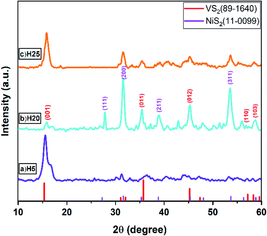
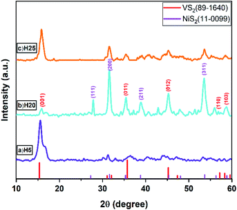
The crystallographic patterns of the as-prepared samples were investigated by XRD analysis, whose results are shown in Fig. 1. The five main peaks of the VS2 structure are exhibited at 15.38°, 35.74°, 45.23°, 57.4° and 58.32°, corresponding to the (001), (011), (012), (110), and (103) crystal planes, respectively. Observed residue peaks related to the NiS2 structure were located at 27.2°, 31.6°, 38.8° and 53.8°, which can be attributed to the (111), (200), (211), and (311) crystal planes, respectively. The dominant crystal plane direction for the VS2 phase is (001) for both the H5 and H25 samples, and it changes to the (012) plane for the H20 sample. Furthermore, the superior crystal plane for the NiS2 phase is the (311) direction for the H5 sample, while it changes to (200) for the H20 and H25 samples. As each crystal structure displays high peak intensity, it suggests good crystallinity and the complete formation of crystal planes.
 |
| | Fig. 1 XRD patterns of the VS2–NiS2 hybrid samples. | |
FESEM images analysis
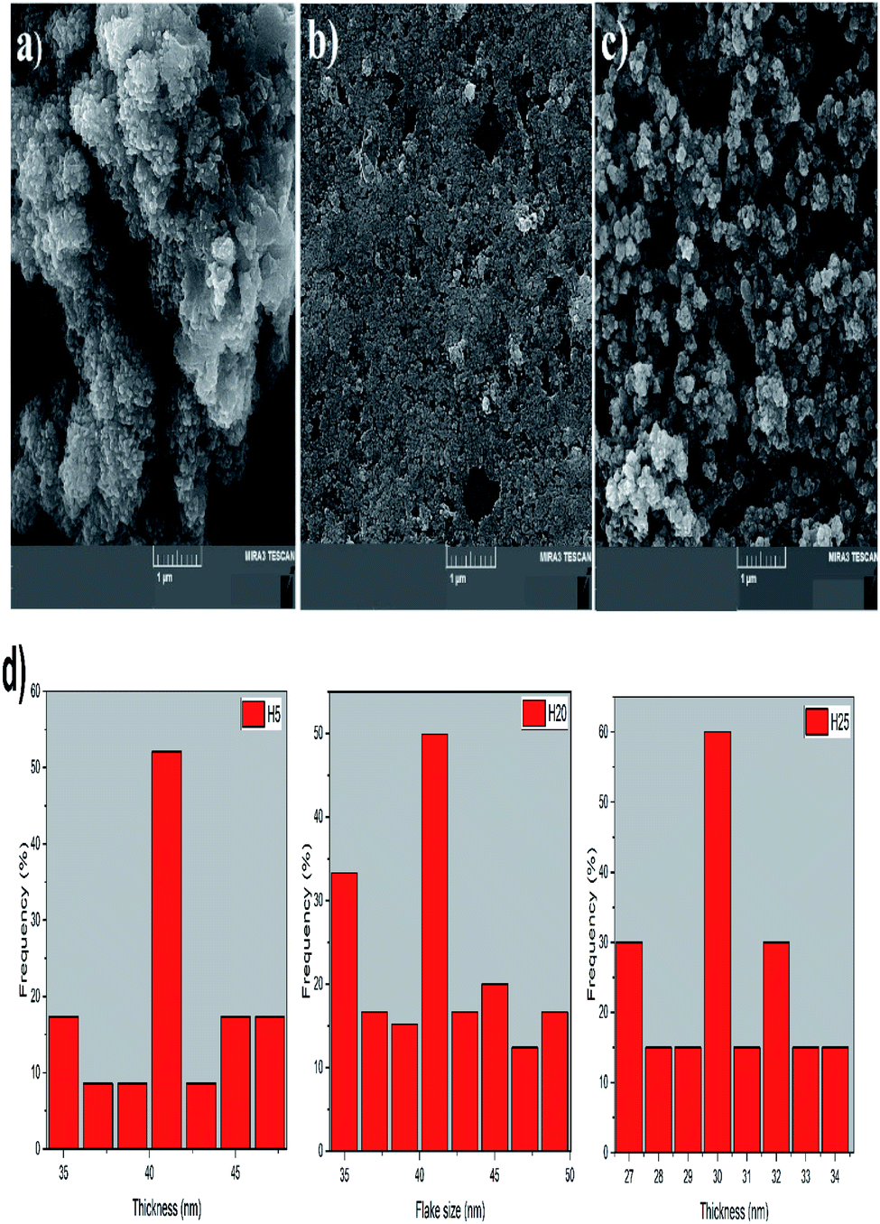
The characterization of the morphology of the diverse hybrid nanostructures is shown in Fig. 2(a–c). As we know, the morphology of the pure VS2 structure is a sheet and laminated structure, while the morphology is altered by addition of the NiS2 phase to the main structure. The microflower structure of the H5 sample is apparent. Thus, the size of the sheets has reduced and the morphology has changed to a flower-like structure. The size of the sheets decreases by increasing the amount of the NiS2 phase in the hybrid nanostructure and the nanoflakes of this structure are observed for the H20 sample. The process of sheet size reduction continues until the nanoflowers of the H25 sample are formed, which indicates the change of size and morphology. The size distribution histogram for the thickness of the sheets or flake size is exhibited in Fig. 2(d). The histogram indicates that the maximum distribution of thickness is about 41 and 30 nm for the H5 and H25 sample, respectively. However, the flake size is considered and measured for the H20 sample due to its smaller sheet size. Therefore, the largest amount of flake size distribution is located at about 41 nm.
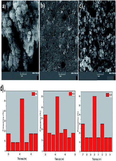 |
| | Fig. 2 FESEM images of (a) H5, (b) H20, and (c) H25. (d) Size distribution histogram of all samples. | |
UV-visible spectroscopy
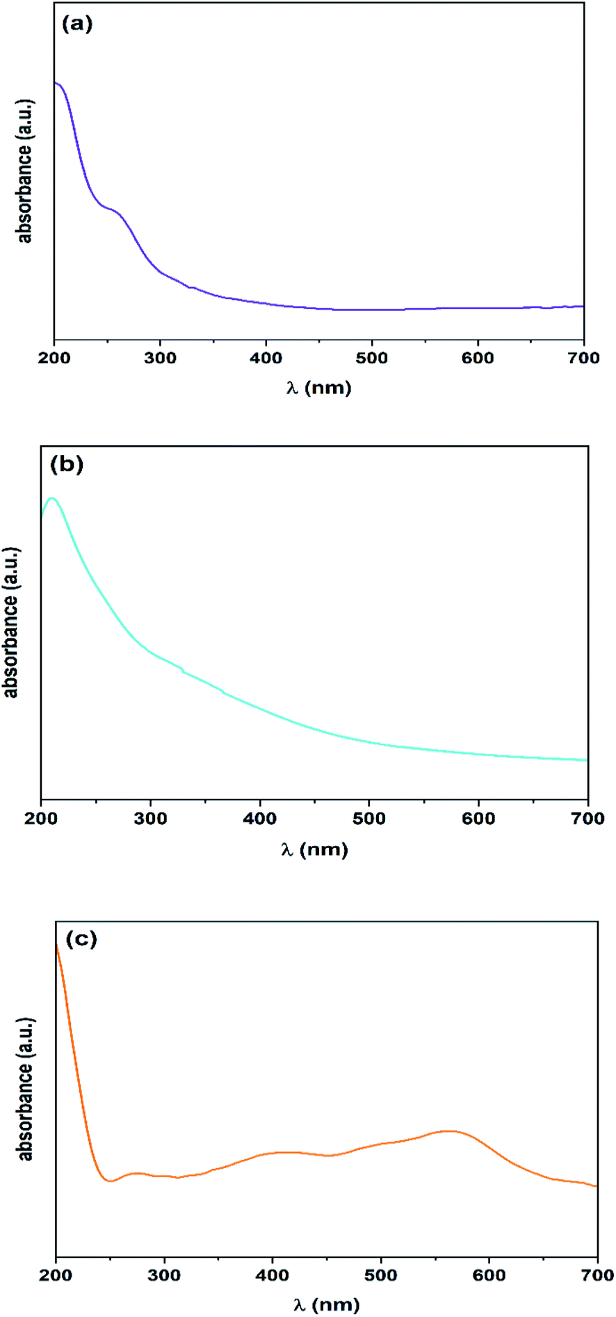
UV-visible spectroscopy was performed to investigate linear absorption in the UV-visible region (200–700 nm) for different prepared samples (Fig. 3). Three original excitonic peaks attributed to the VS2 structure are found at 206, 260, and 316 nm. Moreover, the first excitonic peak for the NiS2 phase is at about 350 nm and the second one is positioned in the wavelength region of 550–600 nm. The absorption band edge is shifted to a higher wavelength (red-shift) compared to that in pure VS2, which indicates the effect of the nickel sulfide structure and its different concentrations in the hybrid nanostructure.
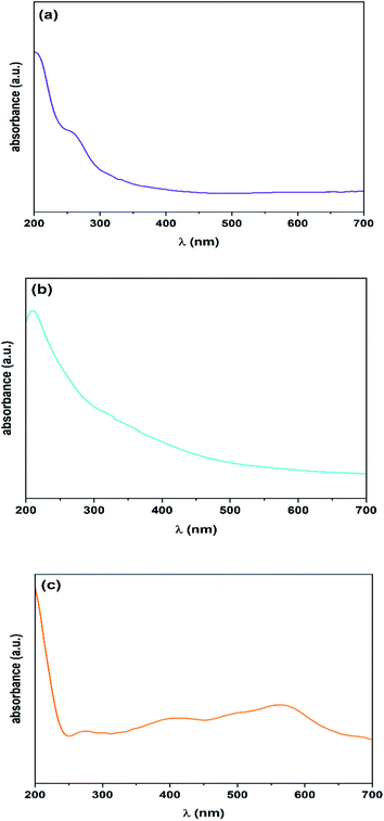 |
| | Fig. 3 UV-visible spectra of the hybrid nanostructures: (a) H5, (b) H20, and (c) H25. | |
FTIR spectroscopy
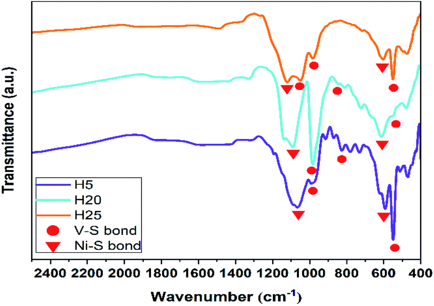
The investigation of IR active vibrational modes and further perusal of the structure of the as-prepared hybrid nanostructures was conducted by FTIR spectroscopy, as shown in Fig. 4. The associated vibrational modes of the VS2 structure are in the 500–1000 cm−1 wavenumber region. The vibrational modes at approximately 540, 830, and 960 cm−1 are associated with S–V–S bonding, the double bonding of S![[double bond, length as m-dash]](https://www.rsc.org/images/entities/char_e001.gif) S, and the double bonding of VS, respectively. Moreover, the presence of the two modes at around 590 and 1066 cm−1 refers to the vibrational modes of Ni–S bonding. Therefore, observation of these vibrational modes proves the presence of the two structural phases VS2 and NiS2. Additionally, all mentioned vibrational modes are shifted to lower or higher wavenumbers (red- or blue-shift) according to the size and morphology of the hybrid nanostructures.
S, and the double bonding of VS, respectively. Moreover, the presence of the two modes at around 590 and 1066 cm−1 refers to the vibrational modes of Ni–S bonding. Therefore, observation of these vibrational modes proves the presence of the two structural phases VS2 and NiS2. Additionally, all mentioned vibrational modes are shifted to lower or higher wavenumbers (red- or blue-shift) according to the size and morphology of the hybrid nanostructures.
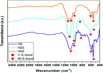 |
| | Fig. 4 FTIR spectra of the VS2–NiS2 hybrid samples. | |
Linear optical parameters
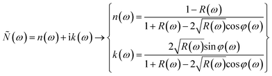
A KK method based on the reflectance spectrum data R(ω) was applied to determine the optical parameters of the samples. The complex refractive index Ñ(ω) including the real (n(ω)) and imaginary (k(ω)) part was determined as follows:| |
 | (1) |
The phase change between the incidence and reflected signal occurs at a specific frequency and is related to the φ(ω) parameter. Additionally, the components of the complex dielectric function ε(ω) were defined based on the components of Ñ(ω)as follows:
| |
 | (2) |
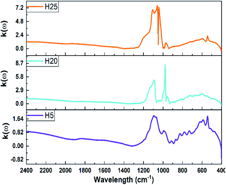
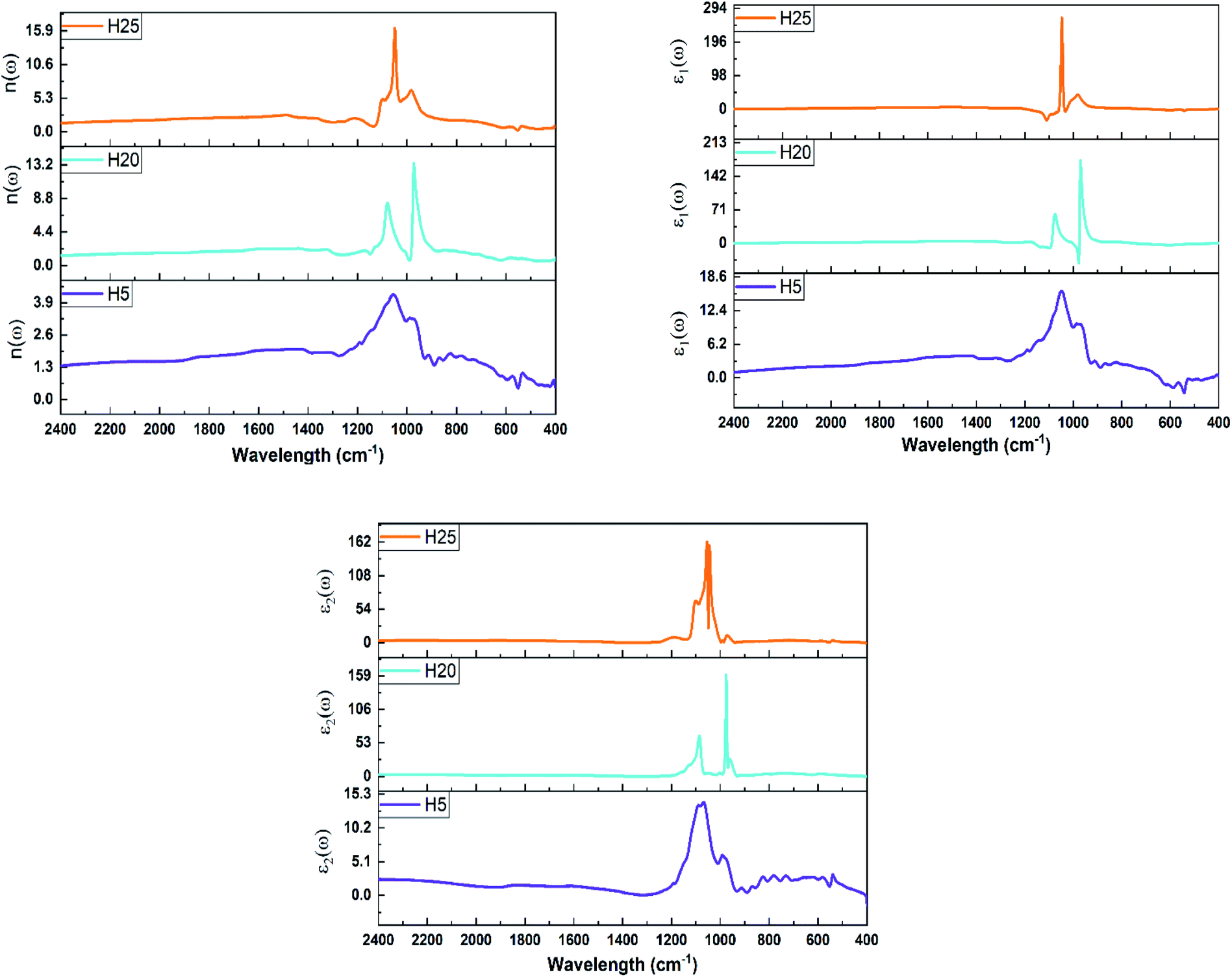
Two components of the Ñ(ω) index of the as-prepared hybrid nanostructures are compared in Fig. 5. The results demonstrate that the highest value of both the real and imaginary parts are enhanced by increasing the amount of NiS2 phase in the hybrid nanostructure. The maximum values of n(ω) are positioned at the wavenumber region of 900–1100 cm−1. Moreover, the maximum values for k(ω) are presented at the interval of wavenumbers 800–1200 cm−1. The peak position of n(ω) moves to lower wavenumbers from the H5 to H20 sample and then higher wavenumbers from the H20 to H25 sample. Thus, the peak position was altered by changing the proportion of the NiS2 phase in the hybrid nanostructures. The peak position displacement for k(ω) follows a blue-shift trend from the H5 to H25 sample. The maximum values for the H25 sample are 3.75 and 4.13 times higher than n(ω) and k(ω) for the H5 sample, respectively.
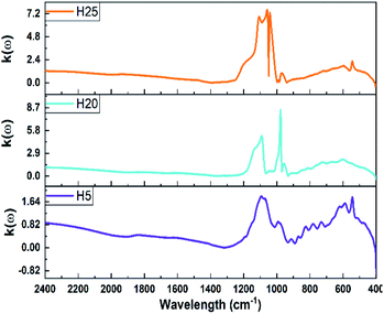 |
| | Fig. 5 Refractive index (n(ω)) and extinction coefficient (k(ω)) of the VS2–NiS2 hybrid samples. | |
The real and imaginary parts of the dielectric function for the VS2–NiS2 hybrid samples are shown in Fig. 6. According to the obtained results, the peak position of the real part ε1(ω) is in the 900–1100 cm−1 wavenumber region. Additionally, the peak of the ε1(ω) plot is first shifted to a lower wavenumber and then a higher wavenumber by increasing the proportion of the NiS2 phase in the hybrid nanostructure samples. The maximum value of ε1(ω) increases 16.67 times from the H5 to H25 sample. The maximum value of the ε2(ω) plot is situated in the range of 900–1100 cm−1 and the peak position has the same behaviour as the peak position for ε1(ω). Furthermore, the highest value of ε2(ω) for the H25 sample is 11.56-fold that of the H5 sample. Finally, the amount of NiS2 phase in the hybrid nanostructures affects the linear optical properties and the related defined indexes of the as-prepared samples.
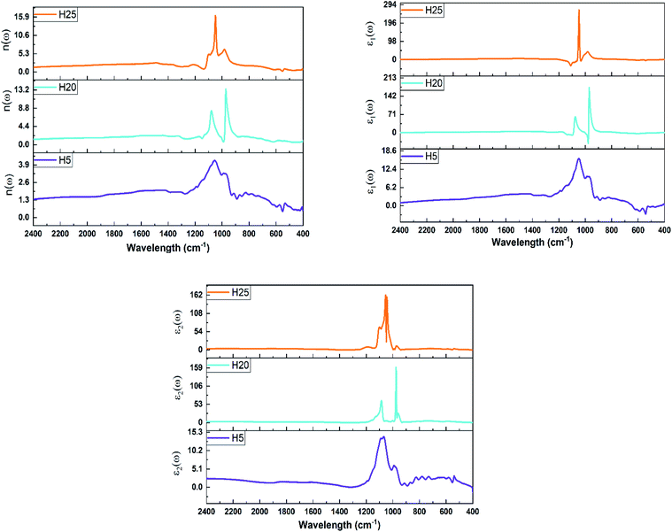 |
| | Fig. 6 Real (ε1(ω)) and imaginary (ε2(ω)) parts of the dielectric function for the VS2–NiS2 hybrid samples. | |
Nonlinear optical properties: Z-scan investigation
The nonlinear optical properties of materials can be evaluated by different techniques such as nonlinear interferometry. We used the Z-scan technique as an accurate and simple method for evaluating the third-order nonlinear optical properties of our different samples. In the Z-scan array, there are different main parts: an Nd:YAG laser as an optical source (CW-laser, 532 nm), a lens for focusing the laser beam, a quartz cuvette containing the dispersed sample, an aperture and a detector. Water was used as the host dispersant medium and the power of the source laser was stabilized to ensure the accuracy of the results. Two types of Z-scan study were applied for the evaluation of the nonlinear optical properties: open aperture (OA) for the nonlinear absorption coefficient (β), and closed aperture (CA) for the nonlinear refractive index (n2). As we know, induced absorption and refraction changes by incident laser irradiation are described via the following relationships: α(I) = α0 + βI and n(I) = n0 + n2I.
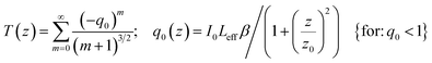
The β parameter is calculated by the best fitting of the OA Z-scan data with the following equation:
| |
 | (3) |
By solving the summation and considering a very small linear absorption constant (α0 ≪ 1), we obtain the following relation:
| |
 | (4) |
In this equation,
Leff is the effective thickness of the sample,
L is the thickness of the sample,
z0 = π
ω02/
λ is the diffraction length of the laser beam,
λ is the wavelength of the laser, and
I0 is the intensity of the laser beam at the focus point
z = 0.
24
Meanwhile, the n2 parameter can be obtained via calculation of the on-axis nonlinear phase shift at the focus (Δφ0). This phase shift was computed by fitting of the CA/OA curve using the following equation:
| |
 | (5) |
T(
z) is the normalized transmittance for the CA/OA curve. Finally, the
n2 index was calculated
via the following equation:
25| |
 | (6) |
OA Z-scan results
Fig. 7 shows the OA Z-scan characterization of the different samples for three different laser powers. There is a downward facing curve in all plots that indicates the positive sign of the nonlinear absorption coefficient. The positive β implies the two-photon absorption phenomenon. This effect originates from the fact that two photons are simultaneously absorbed at equal or different energies, which excites the electrons from the ground state to the excited state (S0–S1). In this process, the transition energy is the sum of both absorbed photons. The observed phenomenon for the nonlinear absorption of the samples is analogous to our previous report for VS2 nanosheets as well as other reported TMDs.23,26–28
 |
| | Fig. 7 Open-aperture Z-scan curves of (a) H5, (b) H20, and (c) H25, with different laser powers (solid line is the fitted curve; P1: 30 mW, P2: 40 mW, P3: 50 mW). | |
The valley deepened by reducing the power of the source laser. Therefore, the β values decrease and the values are as high as 10−3 cm W−1. The comparison between these hybrid VS2–NiS2 nanostructured samples with the pure VS2 phase demonstrates that the presence of the NiS2 phase in the hybrid nanostructure promotes the nonlinear optical responses and their nonlinear absorption coefficients are four orders of magnitude higher than that of pure VS2. In fact, the preparation of hybrid structures makes it possible to increase the density of states for electrons and enhance the interaction between light and matter, ultimately improving the NLO properties. The maximum β values for the different hybrid nanostructures are 9.7 × 10², 14.6 × 10², and 125.8 × 10²-fold greater than that of the pure VS2 phase for H5, H20, and H25, respectively. Therefore, the shape of the nanostructure and electronic alignment alterations affect the nonlinear optical properties and cause the promotion of these properties for utilization in the field of photonics.
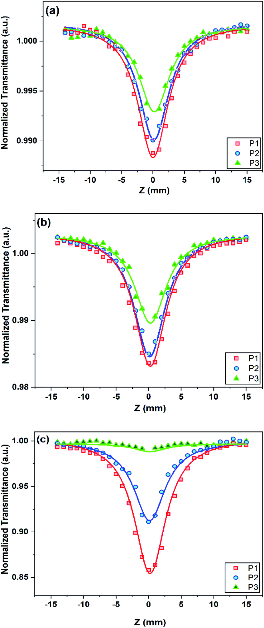
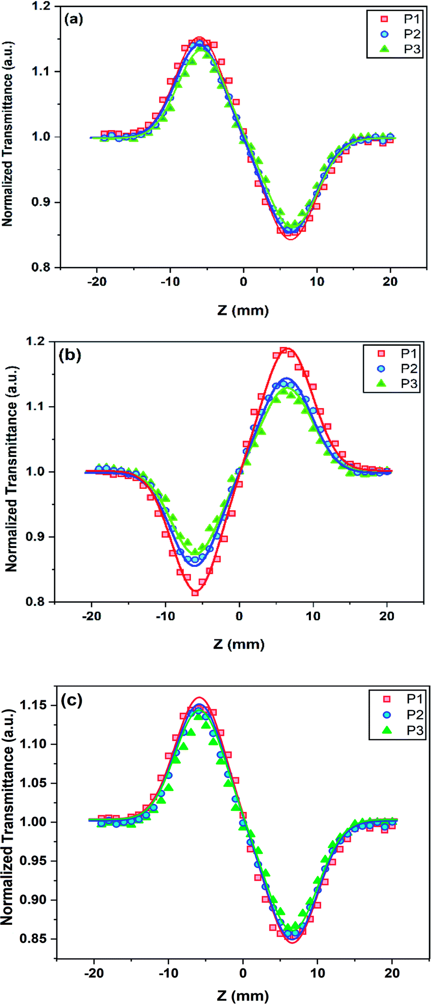
CA Z-scan results
As shown in Fig. 8, the nonlinear refractive index behaviour of the hybrid samples changes and there is an upward facing curve accompanied by a downward facing curve for the H5 and H25 samples. Unlike the other samples, there is a valley followed by a peak for the H20 sample. Thus, the sign of n2 is negative for the H5 and H25 samples, which indicates their self-defocusing nonlinear optical behaviour, while there is a positive nonlinear refractive index for the H20 sample, which implies its self-focusing nonlinear optical behaviour.
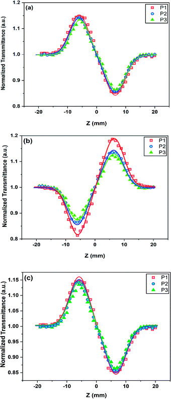 |
| | Fig. 8 Closed-aperture Z-scan curves of (a) H5, (b) H20, and (c) H25, with different laser powers (solid line is the fitted curve; P1: 30 mW, P2: 40 mW, P3: 50 mW). | |
As mentioned in eqn (5) and (6), the difference between the height of the valley and peak reduces by increasing the laser power and hence the n2 index decreases for the samples. The magnitude of the nonlinear refractive index is in the order of 10−9 cm2 W−1, which is four orders higher than the reported results for the pure VS2 phase. These changes demonstrate the effect of the simultaneous presence of the NiS2 and VS2 phases in the hybrid nanostructure and the different proportion of the NiS2 phase in the hybrid nanostructure exhibits different nonlinear optical responses and behaviours. The calculated third-order nonlinear optical parameters of different hybrid nanostructures are compared in Table 1.
Table 1 Nonlinear optical parameters of different hybrid nanostructures
| Sample |
P0 (mW) |
αa (cm−1) |
Leff (mm) |
ω0 (μm) |
n2 (cm2 GW−1) |
β (cm kW−1) |
σ2PA (×109 GM) |
| α is the total absorption coefficient that depends on the incident laser power intensity. |
| H5 |
30 |
0.056 |
0.99 |
31 |
35.62 |
0.156 |
0.96 |
| 40 |
0.292 |
0.98 |
36 |
32.57 |
0.145 |
0.89 |
| 50 |
0.068 |
0.99 |
42 |
24.23 |
0.141 |
0.87 |
| H20 |
30 |
0.646 |
0.96 |
31 |
43.51 |
0.235 |
1.45 |
| 40 |
0.674 |
0.96 |
36 |
32.02 |
0.223 |
1.38 |
| 50 |
0.040 |
0.99 |
42 |
30.97 |
0.219 |
1.35 |
| H25 |
30 |
0.056 |
0.99 |
31 |
33.55 |
2.025 |
12.55 |
| 40 |
0.292 |
0.98 |
36 |
33.52 |
1.299 |
8.05 |
| 50 |
0.068 |
0.99 |
42 |
34.2 |
0.141 |
0.87 |
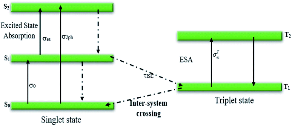
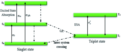
Generally, the nonlinear optical characteristics originate from electronic, molecular, electrostrictive, or thermal effects. When there is a CW-type laser in the Z-scan setup, the thermal effect is the dominant phenomenon for the generation of nonlinear optical responses. The creation of spatial temperature distribution due to the local laser heating in the nonlinear medium leads to the alteration of nonlinear optical properties. Another strategy to describe such changes in these properties is a five-state transition diagram. According to this theory (Fig. 9), the molecules are excited via two photon absorption to the upper vibrational levels S1 or S2 with the related cross sections σ0 or σ2ph under irradiation of the source laser. Next, these excited molecules rest at the S1 state. Due to the existence of the CW-type laser, it is possible that the intersystem transition to T1 occurs and one further excitation to T2 can occur with the cross section σTes. The condition for this type of transition is τpulse ≥ τinter-system.29,30
 |
| | Fig. 9 Schematic of the five-state transition theory. | |
It is worth noting that all nonlinear coefficients reduce with increasing laser power. In fact, the energy redistribution in the intramolecular space for the excited state absorption of the molecules causes the reduction of nonlinear optical parameters with increasing laser power. In other words, some photons are trapped and not allowed to transit; consequently, these nonlinear parameters decrease with increasing laser power.
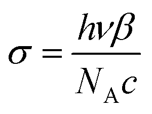
According to the TPA nonlinear phenomena, we evaluated the two-photon absorption cross section (σ2ph) equations as follows:
| |
 | (7) |
where
c is the sample concentration (0.01 M) and
NA is the Avogadro constant.
σ2PA is as high as 10
9 GM. These results reveal that this type of TMD material can be utilized in the optical limiting field as well as in optical modulators. According to our results and study, the data in
Table 2 demonstrate the comparison of the NLO parameters for well-known TMDs (
e.g., MoS
2, WS
2) and the studied hybrid nanostructure VS
2–NiS
2. Thus, the obtained NLO parameters are comparable or greater than those of other reported TMDs.
Table 2 Comparison of the NLO parameters of various reported TMDs and this work
| Material |
λ (nm) |
n2 (cm2 W−1) |
β (cm W−1) |
NLO response |
Ref. |
| MoS2, WS2, NbSe2 |
532 |
— |
3 × 10⁻¹³ to 1.2 × 10⁻⁹ |
SA-RSA |
26 |
| MoTe2/MoS2 |
800 |
— |
555.45 × 10⁻⁹ |
SA |
31 |
| NbS2, ZrTe2 |
532 |
— |
(0.42–0.57) × 10−7 |
SA-RSA |
32 |
| MoS2 |
532 |
(3.11–5.16) × 10−4 |
31.18–145.72 |
SA-TPA |
33 |
| WS2, WSe2, MoS2, Mo0.5W0.5S2 |
1064 |
— |
(1.9–19.1) × 10−9 |
SA-TPA |
34 |
| WS2, WSe2 |
1040 |
3.36 × 10⁻¹² to 1.28 × 10⁻¹⁰ |
(1.81–5.29) × 10−6 |
TPA |
35 |
| MoS2 |
532, 1064 |
— |
(−48.92 to 1151.01) × 10−9 |
SA-RSA |
36 |
| MoS2/PMMA |
800 |
— |
(16.8–970.4) × 10−9 |
RSA |
37 |
| WS2-PMMA |
532 |
— |
(−16.47 to 4.38) × 10−9 |
SA-RSA |
38 |
| MoS2/TiO2 |
700 |
(0.116–3.6) × 10−9 |
— |
SA-TPA |
28 |
| MoS2, WS2 |
1030 |
— |
(0.66–2.28) × 10−6 |
TPA |
39 |
| WS2 |
800 |
— |
(−92 to 0.01) × 10−9 |
SA-RSA |
40 |
| VS2–NiS2 hybrid |
532 |
(24.23–35.62) × 10−9 |
(0.141–2.025) × 10−3 |
TPA |
This work |
VS2-based structures are utilized in many fields such as photoelectrocatalysts, sensors, batteries, and supercapacitors. In all these applications, the speed of electron transfer as well as the optical response is an important issue. In recent years, this structure has been studied with Q-switched lasers and mode lock fiber lasers.16,17 According to our NLO results, this research has potential for further discovery in various optical fields such as Q-switched fiber lasers, ultrafast and mode lock fiber lasers, optical limiting, and cavity dumping in active laser medium. We promoted the NLO coefficients of the VS2 structure via hybridization with the NiS2 structure. The five-state-based two-photon absorption optical phenomenon is one of the reasons for the enhanced NLO response, which plays a critical role in the above-mentioned applications.27,41,42 It is quite pleasing that we achieved such good results via the CW laser Z-scan technique.
Conclusion
In this work, VS2–NiS2 hybrid nanostructures were synthesized via a one-pot hydrothermal method using different concentrations of the NiS2 phase. The morphology of the different hybrid nanostructures was changed by adding different amounts of the NiS2 phase. Thus, the linear optical properties and NLO parameters change under the mentioned conditions. Based on the sensitive Z-scan characterization, the nonlinear β coefficient is as high as 10−3 cm W−1 and the two-photon absorption effect is the main reason for the enhanced nonlinear absorption process. Moreover, the nonlinear n2 indexes are in the order of 10−9 cm2 W−1 and their behaviour is altered from self-defocusing to self-focusing due to the alteration of electronic alignment and morphology. The reduction of NLO parameters with increasing laser power implies the energy loss of photons during the NLO processes and indicates the applicability of these structures in optical limiting fields. Comparison between the nonlinear optical behaviour of the VS2–NiS2 hybrid nanostructures and the pure VS2 phase indicates the excellent potential of these hybrid nanostructures for future photonics and optical application and studies.
Conflicts of interest
There are no conflicts to declare.
Acknowledgements
The authors wish to express their gratitude to the Shahid Rajaee Teacher Training University and Tarbiat Modares University.
References
- J. H. Strait, P. Nene and F. Rana, Phys. Rev. B: Condens. Matter Mater. Phys., 2014, 90, 245402 CrossRef.
- P. Schiettecatte, P. Geiregat and Z. Hens, J. Phys. Chem. C, 2019, 123, 10571–10577 CrossRef CAS.
- K. Wang, J. Wang, J. Fan, M. Lotya, A. O'Neill, D. Fox, Y. Feng, X. Zhang, B. Jiang and Q. Zhao, ACS Nano, 2013, 7, 9260–9267 CrossRef CAS PubMed.
- G.-Q. Jiang, C.-B. Yao, S.-B. Bao and Y. Cai, Opt. Mater., 2020, 106, 109995 CrossRef CAS.
- J. Zhang, M. Ye, S. Bhandari, A. K. M. Muqri, F. Long, S. Bigham, Y. K. Yap and J. Y. Suh, Nanotechnology, 2017, 28, 295301 CrossRef PubMed.
- W. Murray, M. Lucking, E. Kahn, T. Zhang, K. Fujisawa, N. Perea-Lopez, A. L. Elias, H. Terrones, M. Terrones and Z. Liu, 2D Mater., 2020, 7, 45020 CrossRef CAS.
- F. J. F. Löchner, A. George, K. Koshelev, T. Bucher, E. Najafidehaghani, A. Fedotova, D.-Y. Choi, T. Pertsch, I. Staude and Y. Kivshar, ACS Photonics, 2020, 8, 218–227 CrossRef.
- N. Dong, Y. Li, S. Zhang, N. McEvoy, R. Gatensby, G. S. Duesberg and J. Wang, ACS Photonics, 2018, 5, 1558–1565 CrossRef CAS.
- L. Li, R. Lv, S. Liu, X. Wang, Y. Wang, Z. Chen and J. Wang, Laser Phys., 2018, 28, 55106 CrossRef.
- H. Ahmad, S. N. Aidit, J. Mohanraj, S. Sivabalan, K. Thambiratnam, S. I. Ooi and Z. C. Tiu, IEEE J. Quantum Electron., 2018, 54, 1–9 Search PubMed.
- M. Velický and P. S. Toth, Appl. Mater. Today, 2017, 8, 68–103 CrossRef.
- J. Mohanraj, V. Velmurugan and S. Sivabalan, Opt. Mater., 2016, 60, 601–617 CrossRef CAS.
- L. M. Malard, T. V Alencar, A. P. M. Barboza, K. F. Mak and A. M. De Paula, Phys. Rev. B: Condens. Matter Mater. Phys., 2013, 87, 201401 CrossRef.
- N. Dong, Y. Li, Y. Feng, S. Zhang, X. Zhang, C. Chang, J. Fan, L. Zhang and J. Wang, Sci. Rep., 2015, 5, 14646 CrossRef CAS PubMed.
- M. Taghinejad, Z. Xu, H. Wang, H. Taghinejad, K. Lee, S. P. Rodrigues, A. Adibi, X. Qian, T. Lian and W. Cai, Small, 2020, 16, 1906347 CrossRef CAS PubMed.
- L. Li, L. Pang, Q. Zhao, Y. Wang and W. Liu, Nanophotonics, 2020, 9, 2569 CAS.
- L. Pang, L. Li, R. Wang, Q. Zhao, W. Liu, R. Wu and Y. Lv, Nanotechnology, 2020, 32, 15202 CrossRef PubMed.
- H. Yang, Y. Li, Z. Yang, X. Shi, Z. Lin, R. Guo, L. Xu, H. Qu and S. Zhang, Vacuum, 2020, 174, 109176 CrossRef CAS.
- S. Li, Y. Yin, Q. Ouyang, G. Ran, Y. Chen, E. Lewis, G. Farrell, M. Tokurakawa, S. W. Harun and P. Wang, Opt. Express, 2019, 27, 19843–19851 CrossRef CAS PubMed.
- P. Wang, H. Zhang, Y. Yin, Q. Ouyang, Y. Chen, E. Lewis, G. Farrell, M. Tokurakawa, S. W. Harun and C. Wang, Opt. Laser Technol., 2020, 132, 106492 CrossRef CAS.
- X. Han, Y. Zheng, S. Chai, S. Chen and J. Xu, Nanophotonics, 2020, 9, 1787–1810 CrossRef CAS.
- S. Dong, C. Zhang, Y. Zhou, X. Miao, T. Zong, M. Gu, Z. Zhan, D. Chen, H. Ma and W. Gui, Nanomaterials, 2021, 11, 1648 CrossRef CAS PubMed.
- M. Parishani, M. Nadafan and R. Malekfar, J. Opt. Soc. Am. B, 2021, 38, 1586–1592 CrossRef.
- B. C. Swain, A. K. Das and U. Tripathy, Spectrochim. Acta, Part A, 2019, 223, 117319 CrossRef PubMed.
- M. D. Zidan, M. B. Alsous, A. W. Allaf, A. Allahham, A. Al-Zier and H. Rihawi, Optik, 2016, 127, 2566–2569 CrossRef CAS.
- K. Zhou, M. Zhao, M. Chang, Q. Wang, X. Wu, Y. Song and H. Zhang, Small, 2015, 11, 694–701 CrossRef CAS PubMed.
- Y. Li, N. Dong, S. Zhang, X. Zhang, Y. Feng, K. Wang, L. Zhang and J. Wang, Laser Photonics Rev., 2015, 9, 427–434 CrossRef CAS.
- X. Li, K. Hu, B. Lyu, J. Zhang, Y. Wang, P. Wang, S. Xiao, Y. Gao and J. He, J. Phys. Chem. C, 2016, 120, 18243–18248 CrossRef CAS.
- U. Tripathy and P. B. Bisht, J. Opt. Soc. Am. B, 2007, 24, 2147–2156 CrossRef CAS.
- S. Jeyaram and T. Geethakrishnan, Opt. Laser Technol., 2017, 89, 179–185 CrossRef CAS.
- C. Quan, C. Lu, C. He, X. Xu, Y. Huang, Q. Zhao and X. Xu, Adv. Mater. Interfaces, 2019, 6, 1801733 CrossRef.
- M. E. Maldonado, A. Das, A. M. Jawaid, A. J. Ritter, R. A. Vaia, D. A. Nagaoka, P. G. Vianna, L. Seixas, C. J. S. de Matos and A. Baev, ACS Photonics, 2020, 7, 3440–3447 CrossRef CAS.
- S. Bayesteh, S. Z. Mortazavi and A. Reyhani, J. Phys. D: Appl. Phys., 2018, 51, 195302 CrossRef.
- S. Bikorimana, P. Lama, A. Walser, R. Dorsinville, S. Anghel, A. Mitioglu, A. Micu and L. Kulyuk, Opt. Express, 2016, 24, 20685–20695 CrossRef CAS PubMed.
- N. Dong, Y. Li, S. Zhang, N. McEvoy, X. Zhang, Y. Cui, L. Zhang, G. S. Duesberg and J. Wang, Opt. Lett., 2016, 41, 3936 CrossRef CAS PubMed.
- M. Shi, N. Dong, N. He, Y. Wan, H. Cheng, M. Han, J. Wang and Y. Chen, J. Mater. Chem. C, 2017, 5, 11920–11926 RSC.
- G. Liang, L. Tao, Y. H. Tsang, L. Zeng, X. Liu, J. Li, J. Qu and Q. Wen, J. Mater. Chem. C, 2019, 7, 495–502 RSC.
- B. M. Szydłowska, A. Graf, A. Kelly, W. J. Blau, M. C. Gather, J. Zaumseil and C. Backes, J. Mater. Chem. C, 2020, 8, 10805–10815 RSC.
- S. Zhang, N. Dong, N. McEvoy, M. O'Brien, S. Winters, N. C. Berner, C. Yim, Y. Li, X. Zhang and Z. Chen, ACS Nano, 2015, 9, 7142–7150 CrossRef CAS PubMed.
- C. Lu, D. Yang, J. Ma, M. Luo, Y. Jin and X. Xu, Appl. Surf. Sci., 2020, 532, 147409 CrossRef CAS.
- Z. Niu, T. Feng, T. Li, K. Yang, J. Zhao, G. Li, D. Li, S. Zhao, W. Qiao and H. Chu, Nanomaterials, 2021, 11, 2605 CrossRef CAS PubMed.
- P. Hu, J. Mao, H. Nie, R. Wang, B. Zhang, T. Li, J. He and K. Yang, Molecules, 2021, 26, 4303 CrossRef CAS PubMed.
|
| This journal is © The Royal Society of Chemistry 2022 |
Click here to see how this site uses Cookies. View our privacy policy here. 
 Open Access Article
 This Open Access Article is licensed under a Creative Commons Attribution-Non Commercial 3.0 Unported Licence
 a,
Marzieh Nadafan
a,
Marzieh Nadafan