
 Open Access Article
 This Open Access Article is licensed under a Creative Commons Attribution-Non Commercial 3.0 Unported Licence
Sample preparation induced phase transitions in solution deposited copper selenide thin films
Bar Koren†
*ab,
Ofir Friedman† *ab,
Nitzan Mamanb,
Shmuel Hayunab,
Vladimir Ezerskyb and
Yuval Golanab
*ab,
Nitzan Mamanb,
Shmuel Hayunab,
Vladimir Ezerskyb and
Yuval Golanab
aDepartment of Materials Engineering, Ben-Gurion University of the Negev, Beer-Sheva 8410501, Israel. E-mail: ygolan@bgu.ac.il
bIlse Katz Institute for Nanoscale Science and Technology, Ben-Gurion University of the Negev, Beer-Sheva 8410501, Israel
First published on 21st December 2021
Abstract
Thin films of CuSe were deposited onto GaAs substrate. XRD showed that the as-deposited films were of the Klockmannite (CuSe – P63/mmc 194) phase with lattice parameters a0 = b0 = 0.3939 nm, c0 = 1.7250 nm; however, electron diffraction in the TEM surprisingly indicated the β-Cu2−xSe phase (Cu1.95Se – R![[3 with combining macron]](https://www.rsc.org/images/entities/char_0033_0304.gif) m 166) with lattice parameters a0 = b0 = 0.412 nm, c0 = 2.045 nm. The discrepancy originated from the specimen preparation method, where the energy of the focused ion beam resulted in loss of selenium which drives a phase transition to β-Cu2−xSe in this system. The same phase transition was observed also upon thermal treatment in vacuum, as well as when the 200 keV electron beam was focused on a powder sample in the TEM. The initial phase can be controlled to some extent by changing the composition of the reactants in solution, resulting in thin films of the cubic α-Cu2−xSe (Cu1.95Se – Fmm) phase co-existing together with the β-Cu2−xSe phase.
m 166) with lattice parameters a0 = b0 = 0.412 nm, c0 = 2.045 nm. The discrepancy originated from the specimen preparation method, where the energy of the focused ion beam resulted in loss of selenium which drives a phase transition to β-Cu2−xSe in this system. The same phase transition was observed also upon thermal treatment in vacuum, as well as when the 200 keV electron beam was focused on a powder sample in the TEM. The initial phase can be controlled to some extent by changing the composition of the reactants in solution, resulting in thin films of the cubic α-Cu2−xSe (Cu1.95Se – Fmm) phase co-existing together with the β-Cu2−xSe phase.
Introduction
Copper selenide thin films are of particular interest due to their wide direct band-gap, and diverse crystallographic structures depending on their method of preparation.1–4 These films, therefore, have potential applications in highly efficient solar cells,5 optical filtering,6–8 and superionic conductors.9–11 Copper selenide is attractive for thermoelectric and solar energy conversion due to its low resistivity, and is used in p–n heterojunction solar cell devices as a p-type layer joined with an appropriate n-type material. In addition, annealed copper selenide thin layers showed improved photoelectrochemical performance compared to non-annealed films, with an optical band-gap of 2.74 eV for the as-deposited and 2.66 eV for the annealed films.12Copper selenide has 5 main phases: Klockmannite CuSe, berzelianite (α-Cu2−xSe, x ≈ 0.2 – Fmm 225), and umangite (usually formulated as Cu3Se2;2,13 P![[4 with combining macron]](https://www.rsc.org/images/entities/char_0034_0304.gif) 21m [113]). Additional phases are orthorhombic marcasite CuSe2 (Pnnm 58), and β-Cu1.95Se (Cu1.95Se – Rm 166).14,15 Interestingly, Cu2−xSe can exist in 4 forms (cubic berzelianite, tetragonal, orthorhombic or monoclinic phase), with x = 0.18–0.25.13,15,16 The phase diagram is provided in Fig. 1.17
21m [113]). Additional phases are orthorhombic marcasite CuSe2 (Pnnm 58), and β-Cu1.95Se (Cu1.95Se – Rm 166).14,15 Interestingly, Cu2−xSe can exist in 4 forms (cubic berzelianite, tetragonal, orthorhombic or monoclinic phase), with x = 0.18–0.25.13,15,16 The phase diagram is provided in Fig. 1.17
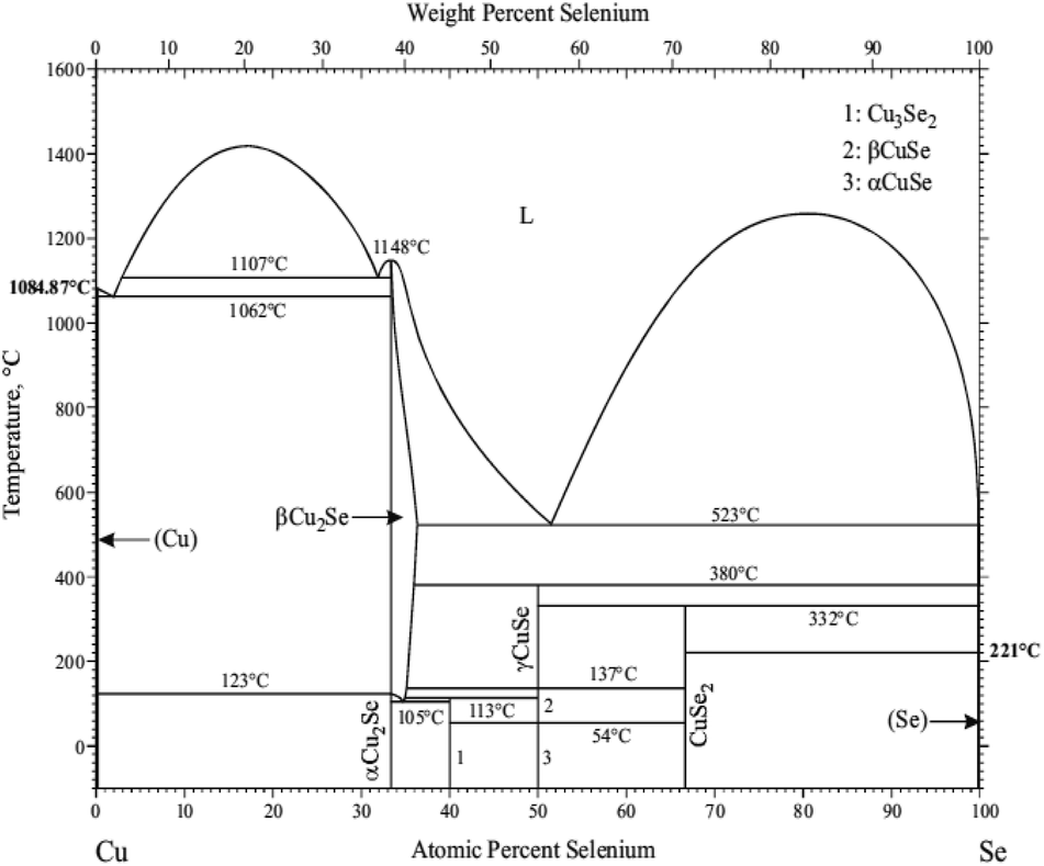 | ||
| Fig. 1 The Cu–Se binary phase diagram.17 Reprinted with permission from Copyright Clearance Center's RightsLink®. | ||
The main phases of interest for the present study article are Klockmannite, cubic berzelianite (α-Cu2−xSe) and the rhombohedral β-Cu1.95Se phases. Klockmannite has a hexagonal structure that is stable under ambient temperature and atmospheric pressure with lattice parameters of a0 = b0 = 0.3939 nm, c0 = 1.7250 nm. The onset of absorption for CuSe is near 1400 nm, with both an indirect bandgap of 0.94 eV and a direct band-gap 1.36 eV.18 The rhombohedral phase (β-Cu2−xSe) was previously grown using chemical vapor transport with iodine and bromine as transport agents, with lattice parameters a0 = b0 = 0.4123 nm, c0 = 2.0449 nm.15 An electrochemically reversible transition from the orthorhombic to cubic structure of Cu2−xSe was reported, with corresponding band-gap values of 1.63 and 1.31 eV, respectively.4
Focused ion beam (FIB) milling and polishing is a commonly used approach for transmission electron microscopy (TEM) sample preparation. However, artifacts that are generated due to Ga+ ion bombardment in the FIB are not commonly reported. For example, it was reported that milling of copper with Ga+ ions resulted in a phase transformation from Cu to Cu3Ga.19,20 In particular, structural defects, such as interstitials and vacancies that can be generated as a result of energy transfer from high energy Ga ions may cause alternations in the structure, composition and resulting physical properties.20,21
Solution deposition is one of the most common methods for the preparation of copper selenide thin films.2,4,7,9,12,13 Cu2−xSe (cubic berzelianite) was reported to form from solution at ∼25 °C;22 Klockmannite CuSe powder was chemically deposited by the reaction of copper ion (CuCl2·2H2O) 0.5 M with selenium ion (sodium selenosulfate) in the presence of 0.8 M sodium tartrate (C4H4Na2O6).23 Interestingly, a new orthorhombic phase of Cu2−xS (the sulphide analog of copper selenide) was recently reported to result from solution.24 Furthermore, thin films in the tetragonal phase (Cu3Se2) were obtained at 5 °C at a pH of 7.8 with a copper sulfate pentahydrate source (CuSO4·5H2O) 0.1 M with 0.3 M trisodium citrate and 0.2 M sodium selenosulfate (all concentrations indicated above correspond to the final bath composition).25
Monocrystalline GaAs were previously shown to induce epitaxial growth in films grown from solution, a phenomenon we have termed as chemical epitaxy see for example ref. 26–30. The original motivation for this work was to use GaAs wafer substrates to induce epitaxial growth of copper selenide thin films. Nevertheless, the discrepancy between the apparent phase obtained for these films using XRD and TEM led us to a thorough investigation of the effect of sample preparation in inducing a phase transition from the Klockmannite phase (CuSe) to β-Cu2−xSe. We show that the phase transition can be induced by either ion beam radiation, as well as by irradiating the specimen under the focused 200 keV electron beam in the TEM. We monitor the phase transition and explain the mechanism in terms of the stoichiometric ratio between copper and selenium in the films. This study adds to growing evidence showing that extra caution should be taken when studying the structure of materials when specimens are prepared using a focused ion beam in dual beam FIB.
Experimental
Materials
Copper(II) chloride dihydrate (≥99.95%), potassium hydroxide (90.0%), trisodium citrate (>99.0%), sodium sulfite (≥98%), selenium powder (≥99.99%) were purchased from Sigma-Aldrich and used without further purification. Deionized water (DIW) was obtained from a Millipore Direct Q3. Monocrystalline GaAs(100) (epi-polished, ±0.1° miscut, undoped) wafers were purchased from Geo Semiconductor (UK) Ltd and manufactured by AXT Inc. (Fremont, CA). Stock solutions of sodium selenosulfate were prepared by stirring sodium sulfite (0.5 M) and selenium powder (0.2 M) in DIW (50 ml) at 90 °C for 3 h.Substrate preparation and surface treatments
Single-crystal GaAs(100) wafer substrates were cut into 1 × 2 cm2 pieces. The preparation of the cleaning wafers included two steps of 10 min of ultrasonication cleaning (MRS DCS-120H) at ambient temperature in acetone and then with DI water. The substrates were then dried under N2 flow. Three different surface treatments were evaluated, all based on 2.4 mM of KOH in DIW (i) immersion in 2.4 mM of KOH in DIW. (ii) Immersion in 2.4 M KOH to which 50 mM CuCl2 have been added. (iii) Immersion in 2.4 M KOH to which 50 mM Na2SeSO3 have been added. All three different treatments were carried out at 30 °C for 10 min. Solutions were purged with pure N2 for 60 min prior to use.Deposition procedure
Cu2−xSe thin films were deposited in a CD with reagent concentrations of 15 [mM] CuCl2, 20 [mM] KOH, 260 [mM] citrate CH5O(COO)3 and 50 [mM] Na2SeSO3 (sodium selenosulfate). Before the deposition, DIW, CuCl2, Na3CH5O(COO)3 and KOH were added to a 50 ml Pyrex beaker and then purged with pure N2 for 60 min in order to reduce O2 and CO2 concentrations. Next, the surface-treated GaAs slides were mounted epi-side down in the solution at an angle of ca. 70 degrees with respect to the reactor floor using a glass stage and sodium selenosulfate (aged for 1 day) was added to the solution. Depositions were conducted at a temperature of 70 °C, pH 12.3 and duration of 30, 60, and 120 min.24In a second bath employed for obtaining the cubic berzelianite phase, the same deposition procedure described above was used, apart from the final reagent concentrations of 45 [mM] CuCl2 and 16.5 [mM] Na2SeSO3, while temperature and pH were kept unchanged.
Copper selenide powder
Cu2−xSe powder was obtained either by scraping the copper selenide film from the GaAs substrate, or (as specified in the text) by centrifuging the bulk solution for collecting the precipitated powder by using the following procedure: DIW were added to 29 ml of solution in a centrifuge tube to a final volume of 50 ml, and centrifuged at 4000 rpm for 5 min. The process was repeated after decanting the liquid and refilling with a solution of 1![[thin space (1/6-em)]](https://www.rsc.org/images/entities/char_2009.gif) :1 DIW and isopropanol. Finally, the powder was collected and dried under vacuum for 24 h.
:1 DIW and isopropanol. Finally, the powder was collected and dried under vacuum for 24 h.
Cross-section sample preparation
High-resolution scanning electron microscopy (HRSEM) was carried out using a Thermo-Fisher Verios 460L microscope in plan-view and cross-section sample geometries. Acceleration voltages were 3–10 kV and beam currents were 13–100 pA.
Analytical transmission electron microscopy (TEM) analyses were carried out using a JEOL JEM-2100F operating at 200 kV. Scanning TEM (STEM) images were obtained using a GATAN 806 HAADF STEM detector (high-angle annular dark-field scanning transmission electron microscopy). Where indicated in the text, the samples were cooled to −180 °C in the TEM using a dedicated cold holder for in situ analytical TEM analysis.
X-ray photoelectron spectroscopy – the composition of the films was determined using an ESCALAB 250 spectrometer with a monochromatic Al X-ray source (excitation energy 1486.6 eV). The size of the X-ray beam was 500 μm at a base pressure of 10–9 mbar. Survey spectra were recorded with pass energy (PE) of 150 eV and the high-resolution spectra were recorded with a PE of 20 eV. To correct charging effects, the spectra were calibrated relative to the carbon C 1s peak located at 284.8 eV. Graphs from XPS were processed using Thermo-Scientific Avantage software. Depth profiles (DP) were achieved by a sequence of cycles of Ar+ ion bombardment interwoven with XPS measurements from the exposed surface.
Simultaneous thermogravimetry (TGA) and differential scanning analysis (DSC) was carried out using an STA 449 F3 apparatus (Netzsch Selb, Germany). Sample temperature calibration was performed by melting Sn, Ag, and Au standards in alumina crucibles. Simultaneous thermal analysis was carried out by continuous heating at 10 °C min−1 with 10 min isothermal holds at 30 °C and 800 °C in the heating direction, under a stream of Ar flowing at 40 ml min−1. In order to verify the loss of selenium during thermal treatment, SiO2 wool was placed in the exhaust and samples corresponding to different annealing temperatures were analysed ex situ using HRSEM and EDS.
Results and discussion
Effect of substrate surface treatments
CuSe layers were deposited directly onto GaAs(100) substrates which were pre-treated by several different surface treatments as described in the experimental section. Treatment (i) resulted in poor adhesion between the deposited layer and the substrate. Treatment (ii) resulted in good adhesion between the deposited layer and the substrate and a continuous layer was formed on the substrate. Treatment (iii) resulted in a discontinuous layer formed on the substrate. Therefore, it was decided to treat the GaAs substrate with pre-treatment (ii). The advantage of this surface treatment is likely to be due to formation of a thin buffer layer of Cu cations adsorbed on the GaAs substrate, as evident from the XPS spectrum presented in Fig. 2.33 Subsequently, the substrates were pre-treated using pre-treatment (ii), placed in the deposition bath and a thin film of copper selenide was deposited, as detailed in the experimental section.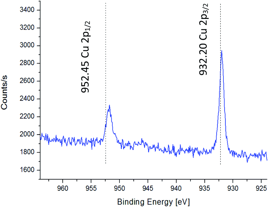 | ||
| Fig. 2 HR-XPS of copper adsorbed on a GaAs(100) substrate following pre-treatment (ii) dashed vertical lines denote the binding energies for Cu2+ according to ref. 33. | ||
The XRD results and corresponding HRSEM images are presented in Fig. 3. The film corresponds to Klockmannite, the hexagonal phase of CuSe as shown in Fig. 3a.
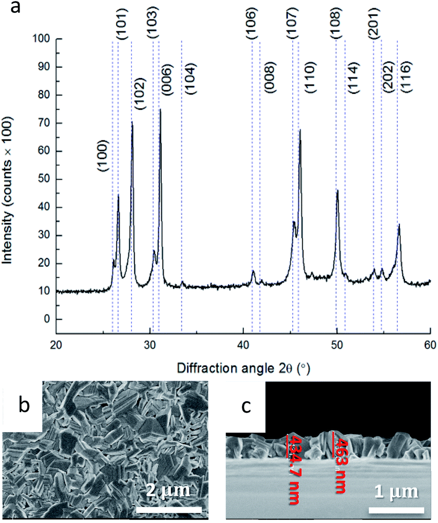 | ||
| Fig. 3 CuSe thin films deposited onto GaAs(100). (a) X-ray diffractogram. Corresponding HRSEM images in (b) plan-view and (c) cross-section. Dashed hairlines in blue correspond to Klockmannite (CuSe – Hex phase), JCPDS file no. 34-0171. | ||
TEM, XRD and SEM analysis of Cu2−xSe on GaAs
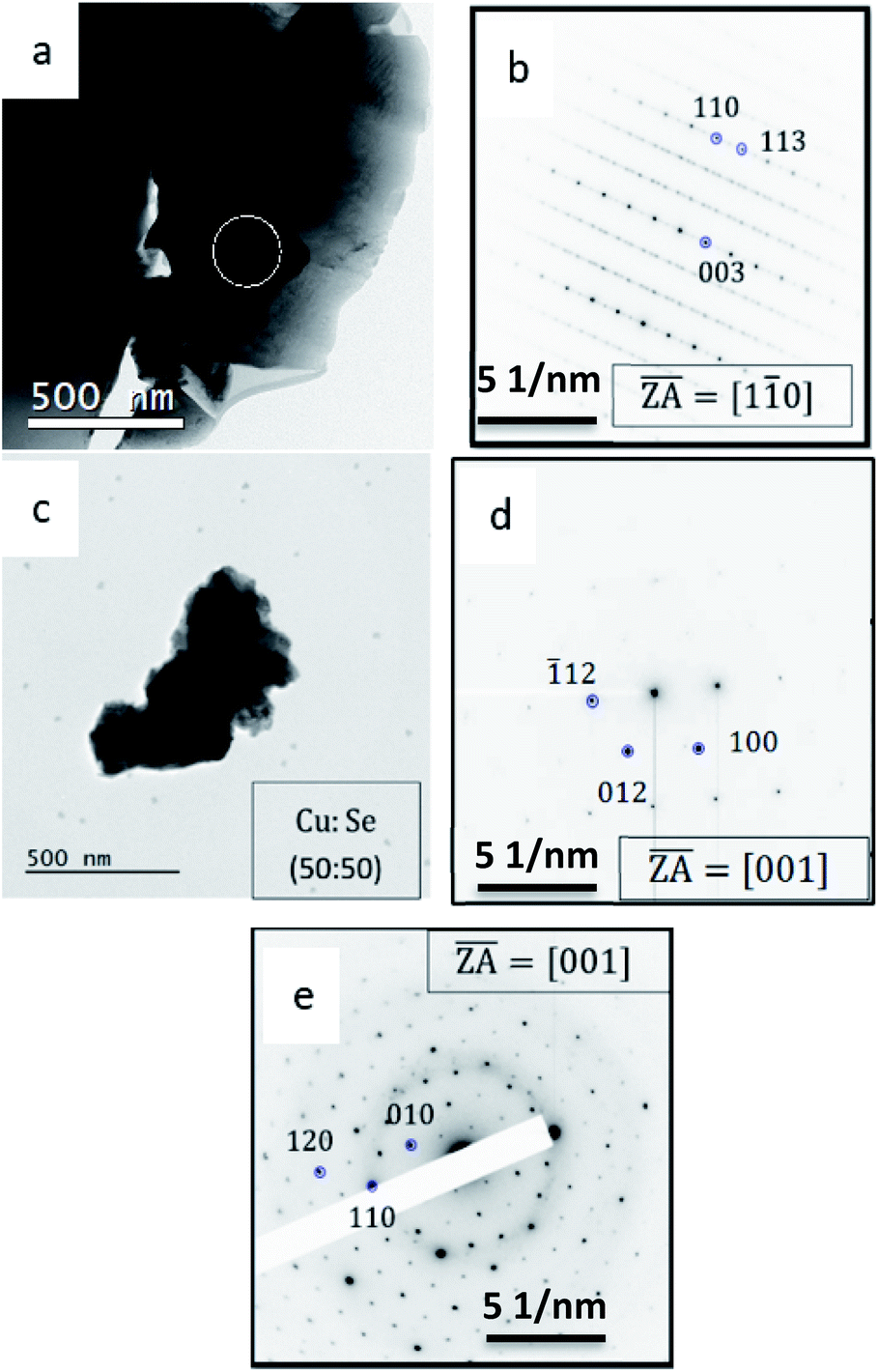
This part of the research was carried out following a discrepancy which arose when copper selenide thin film samples were studied using XRD and TEM. While XRD clearly indicated that the copper selenide grows in the Klockmannite phase of CuSe, ED in the TEM indicated that the sample corresponds to the β-Cu2−xSe form. The discrepancies were settled after realizing that irradiation in the FIB during TEM sample preparation results in an unintentional phase transition from Klockmannite to β-Cu2−xSe. TEM micrographs of a Cu2−xSe particle are shown in Fig. 4a, b and d. Fig. 4a shows a low magnification image of the TEM grid, where one solution deposited Cu2−xSe particle, which was scraped from the substrate onto the grid, is marked in red. The purpose of marking this particle was to follow the irradiation induced phase transition during sample preparation using FIB or PIPS. The corresponding SAED pattern presented in Fig. 4c was indexed to the Klockmannite phase based on prior knowledge.18 In addition, EDS indicated that the copper to selenium ratio is 54:46, fairly close to the 1:1 ratio expected for Klockmannite. The same particle shown in Fig. 4a was identified and sectioned in the FIB, and the cross-section sample was imaged again in the TEM. ED of the same particle (Fig. 4e) indicated that a FIB induced phase transition34 to β-Cu2−xSe clearly took place.15 From EDS, the copper to selenium ratio is 66:34, fairly close to the 2:1 ratio expected for this phase.
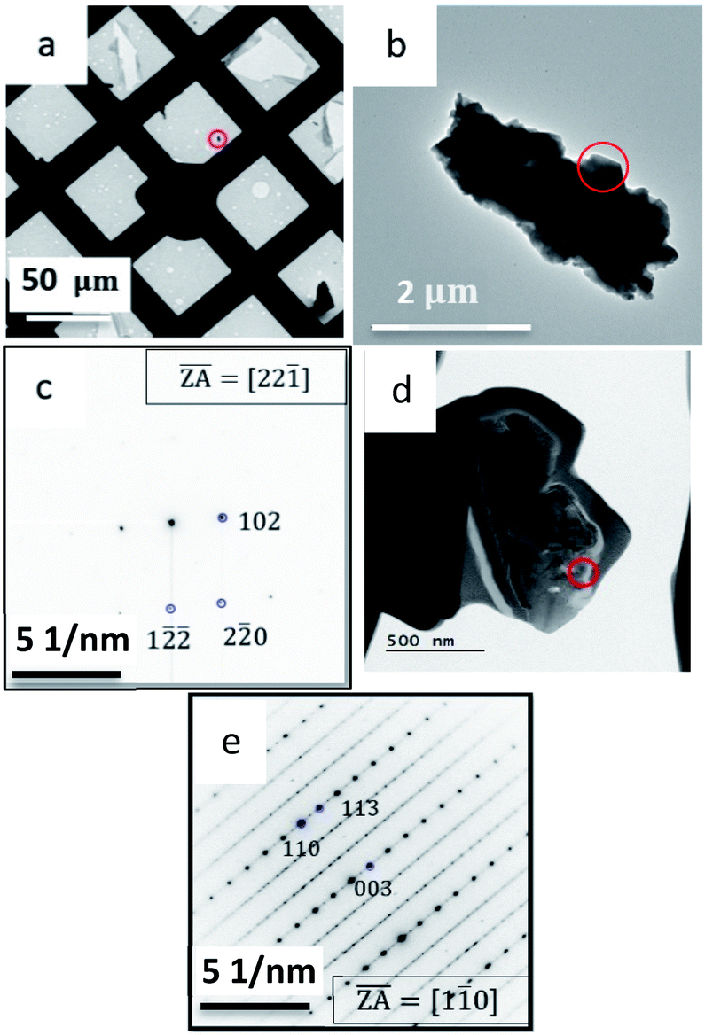 | ||
| Fig. 4 Bright field TEM analysis of CuSe powder (a) low magnification image. (b) Plan-view image taken from the region marked by a red circle in (a). (c) SAED pattern taken from the area marked by a red circle in (b). (d) Cross-section of the same particle shown in (a); the sample was prepared using FIB and (e) SAED pattern taken from the area marked by a red circle in (d). | ||
To exclude the possibility that this phase transition is unique to sample preparation in the FIB, Klockmannite samples were exposed to the ion beam in a Gatan precision ion polishing system (PIPS-II) and to a focused electron beam in the TEM, and both exposures resulted in a phase transition to β-Cu2−xSe phase as presented in Fig. 5a and b. It appears that as a result of the externally applied radiation, the material decomposes and substantial evaporation of Se occurs.17
 | ||
| Fig. 5 TEM analysis of CuSe/GaAs cross-section prepared by mechanical polishing followed by ion milling in the PIPS ion miller (a) bright field micrograph. (b) SAED pattern taken from the area marked by white circle in (a). TEM analysis of a CuSe/GaAs plan-view sample (c) bright field micrograph. (d) SAED pattern taken from (c) and (e) SAED pattern from the same particle shown in (c), after exposure to the focused electron beam in the TEM. | ||
The origin of the weak superstructure reflections seen in Fig. 5b and e has not been unravelled to date as part of the β-Cu2−xSe rhombohedral phase and has been previously attributed to the additional ordering of Cu cations in the structure.15 While the β-phase was reported to correspond to a stoichiometry of Cu1.95Se,15 in our case the considerable loss of Se due to evaporation has driven the phase transition along the 33 at%. Se vertical line in the phase diagram where β-Cu2Se is stable at room temperature. The copper to selenium ratio obtained by EDS from the CuSe particle obtained before exposure to the focused electron beam (Fig. 5c and d) was 1:1, corresponding to the Klockmannite phase, and following exposure of 2 seconds to the beam, the phase transformed into the β-Cu2−xSe with a ratio of ca. 2:1 (Fig. 5e).
While the image in Fig. 5c remained very similar after exposure to the focused electron beam, ED confirmed transition to the β-phase (Fig. 5d and e). It is important to emphasize that while according to the phase diagram the β-phase of copper selenide is a metastable phase at room temperature, the cases described above resulted in phase transition to this metastable phase rather than to the stable cubic α-phase of copper selenide. Subsequently, Klockmannite CuSe powder was heat-treated in vacuum (P = 10 Pa) for 30 min at 400 °C and subsequently cooled down under vacuum to room temperature. Fig. 6 and 7a–c respectively depict XRD and TEM characterization of the heat treated sample. It appears that heating induced a change in composition from a ratio of 1:1 to ca. 2:1 and the structure changed from Klockmannite (as shown in Fig. 6a – dashed red lines) to the stable cubic α-Cu2−xSe (Fig. 6b – blue dashed lines).15
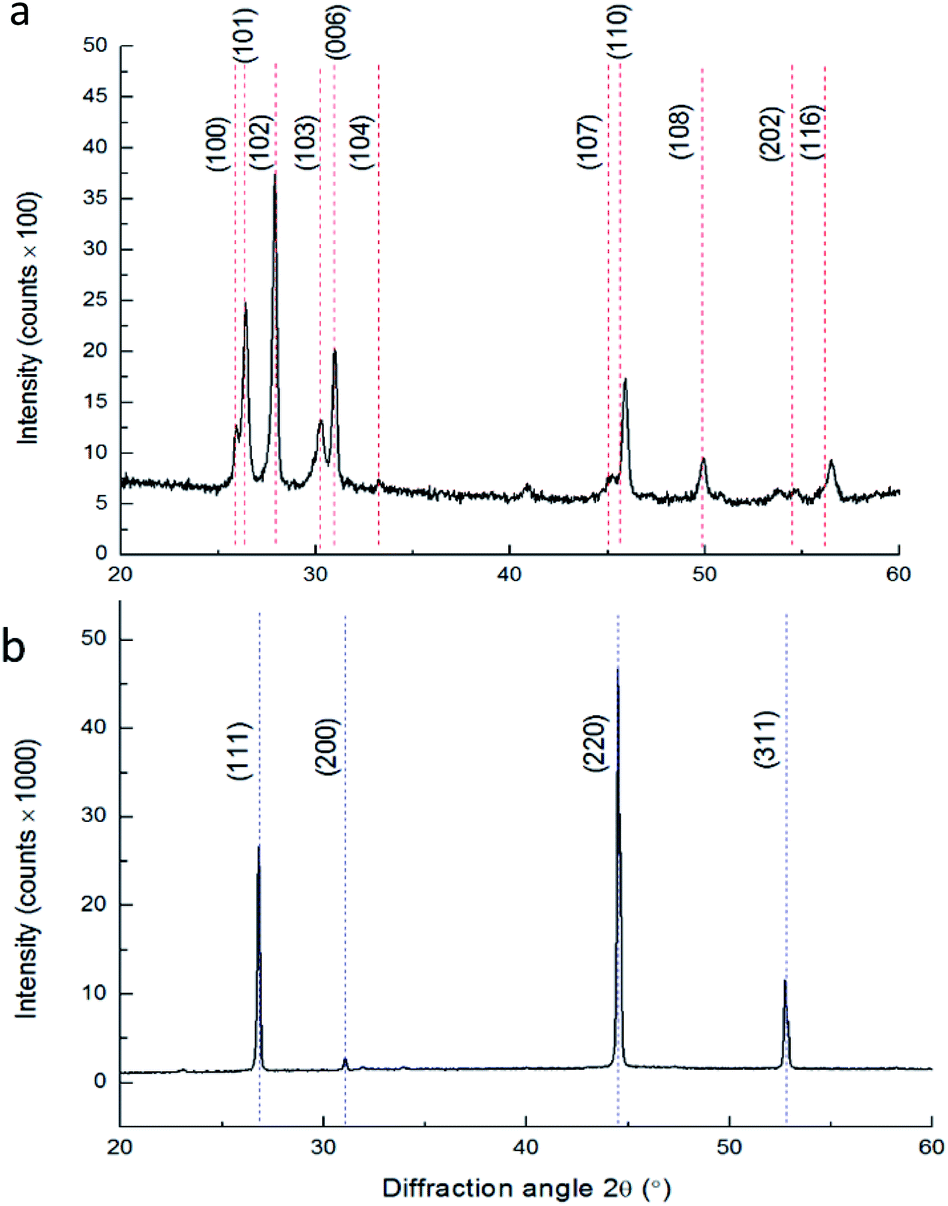 | ||
| Fig. 6 X-ray powder diffractogram of Cu2−xSe (a) before heat treatment. (b) After heat treatment. The dashed red lines represent the peak positions for the Klockmannite phase, while the dashed blue lines represent the peak positions for the cubic α-phase. | ||
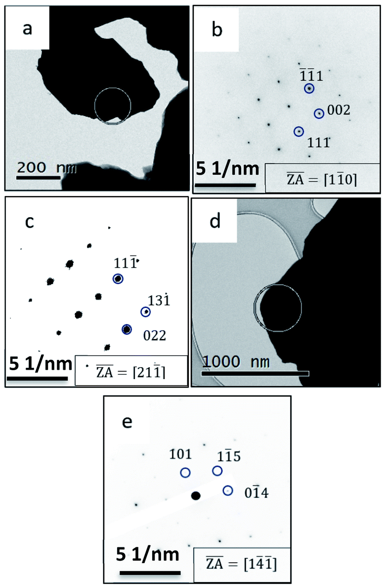 | ||
Fig. 7 TEM analysis of copper selenide particles (a) bright field image of CuSe after heat treatment in vacuum for 30 minutes at a temperature of 400 °C (b) SAED pattern taken from the area marked by white circle in (a), indicating α-Cu2−xSe – Cub with a [1![[1 with combining macron]](https://www.rsc.org/images/entities/char_0031_0304.gif) 0] zone axis (c) SAED pattern taken from the same particle as presented in (a), tilted by 30 degrees, to the [21] zone axis. (d) Another particle from the same powder, following the same annealing process as carried out in (a) and rapid quenching to −180 °C (e) SAED pattern taken from the area marked by white circle in (d), indicating the β-Cu2−xSe phase. 0] zone axis (c) SAED pattern taken from the same particle as presented in (a), tilted by 30 degrees, to the [21] zone axis. (d) Another particle from the same powder, following the same annealing process as carried out in (a) and rapid quenching to −180 °C (e) SAED pattern taken from the area marked by white circle in (d), indicating the β-Cu2−xSe phase. | ||
This phase transformation is expected according to the phase diagram as presented in Fig. 1, which remained stable upon cooling to room temperature. The ED pattern of the particle shown in Fig. 7a shows a ZA of <110> (Fig. 7b), while tilting of the same particle by 30 degrees resulted in a ZA of <211> (Fig. 7c). This confirms the cubic nature of the α-Cu2−xSe phase. Fig. 7d shows a TEM micrograph of the same particle as shown in Fig. 7a, yet this time the particle was cooled to −180 °C in situ in the TEM using liquid nitrogen.
As seen in the ED pattern in Fig. 7e, in this case, a phase transformation has occurred from Klockmannite to the β-Cu2−xSe, which again is readily stabilized at room temperature, as was observed in the case of the radiation-induced phase transitions.15
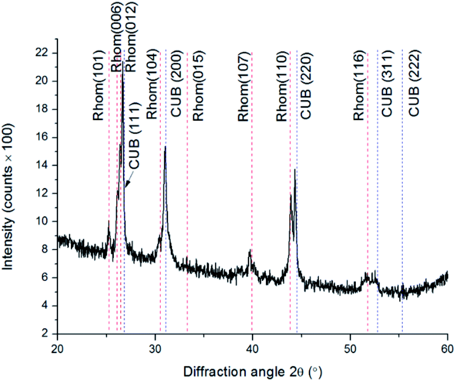
Up to now all as-deposited films were of the Klockmannite phase. However, below we show that it was possible to control the initial phase of the copper selenide obtained by changing the concentrations of the precursors in solution. In the following experiment, we have changed the composition of the precursors to final concentrations of 45 mM CuCl2, and 16.5 mM Na2SeSO3, aiming to test whether this can affect the phase obtained. XRD of this sample presented in Fig. 8 indicated the coexistence of 2 phases. Rietveld refinement gave a phase ratio of 33% β-Cu2−xSe (red lines), and 67% α-Cu2−xSe (blue lines), with no evidence for the presence of the Klockmannite phase.
 | ||
| Fig. 8 X-ray powder diffractogram of Cu2−xSe. Red dashed lines denote β-Cu2−xSe – rhombohedral; blue dashed lines denote α-Cu2−xSe – cubic. | ||
Notably, the peaks from the cubic phase are both larger and sharper, confirming that the majority of the material is in larger grains corresponding to the cubic phase. This can explain the fact that in TEM (Fig. 9) only the cubic α-Cu2−xSe phase was observed, as indicated by the SAED patterns in Fig. 9b and c. Notably, in this case, the cubic phase was directly obtained due to different bath compositions, regardless of irradiation or heat treatments. The SAED pattern in Fig. 9b corresponds to a zone axis of <211>, while tilting the same particle by 30 degrees resulted in a zone axis of <110> as presented in Fig. 9c, as is expected for cubic phase structures.
 | ||
| Fig. 9 Bright field TEM analysis of (a) powder Cu3−xSe (b) SAED pattern taken from the area marked by white circle in (a) and (c) same particle as presented in (b) after tilt with the TEM holder. | ||
CuSe powder in the Klockmannite was heated in Argon atmosphere from room temperature to 800 °C. SEM/EDS analysis of silica wool placed in the furnace exhaust showed that evaporation of the selenium occurs starting from 500 °C. A micrograph of Se coated silica wool is shown in Fig. 10a, where EDS analysis showed roughly 91% silica (silicon and oxygen), and 7% Se coating the silica fibers. At higher temperatures, in a range of 500 °C to 800 °C, condensed droplets of Cu2Se were observed on the silica fibers (Fig. 10b), with a ratio of 18% Cu and 9% Se obtained by EDS analysis.
 | ||
| Fig. 10 HRSEM images of (a) silica wool coated with selenium (b) a Cu2Se droplet deposited on the silica wool. | ||
The TGA and DSC curves of a 1:1 Cu:Se powder (Klockmannite phase) are presented in Fig. 11. At ∼300 °C, there is a significant mass loss of about 16%, confirming the loss of selenium, which drives the phase transformation from the Klockmannite phase to β-Cu2−xSe. The endothermal peaks obtained at low temperatures are related to phase transformation that occurs in the Cu–Se system. Since the starting sample mainly contains the Klockmannite CuSe phase, up to 150 °C no evidence for phase transition can be found. Above this temperature, evaporation of Se begins, and the sample is now comprised of a mixture of CuxSey phases. These phases exhibit phase transitions around 330 to 360 °C (see Fig. 1). Above this temperature, massive mass loss occurs, and the sample transforms to the Cu2−xSe region in the phase diagram. The features at ∼700 °C are likely to be related to the melting of some of the material which did not transform to Cu2Se.
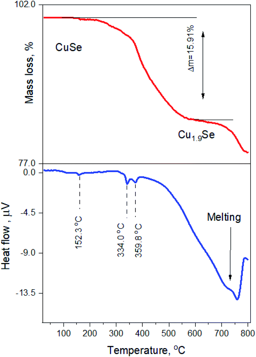 | ||
| Fig. 11 Simultaneous thermal gravimetry and differential scanning calorimetry of Klockmannite CuSe powder. The red line shows mass loss and the blue line represents the heat flow. | ||
Conclusions
The effect of different sample preparation conditions on the phase of CuSe thin films grown using CD turned to be fascinating and unexpected. A pretreatment optimized for covering the substrate surface with a thin Cu buffer layer was found to significantly improve the adhesion of the CuSe layer. Once a layer of CuSe was grown, a contradiction was found between the results from XRD measurements to those from TEM, i.e. the former indicated the Klockmannite phase (hexagonal, CuSe), while the latter indicated the rhombohedral β-Cu2−xSe phase. This was found to be due to the use of specimen preparation methods involving high energy ion beams (FIB and PIPS) or a focused beam of high energy electrons in the TEM. Interestingly, all of the above preparation methods resulted in stabilization of the high-temperature β-Cu2−xSe phase at room temperature. Thermal treatment of Klockmannite followed by slow cooling resulted in the expected room temperature phase of α-Cu2−xSe, while rapid quenching resulted again in the β-Cu2−xSe phase. These results emphasize that extreme caution should be taken when samples in the copper selenide system are studied using focused ion beam specimen preparation methods.Conflicts of interest
There are no conflicts to declare.Acknowledgements
We thank Dr Michael Shandalov for expert assistance in PIPS sample preparation, Dr Yelena Mirsky for expert assistance in XRD and Dr Natalya Froumin for expert help in XPS analyses. This work was supported by the Israel Science Foundation, Grants #156/2014 and #1760/18.References
- R. Seoudi, A. A. Shabaka, M. M. Elokr and A. Sobhi, Optical properties and electrical conductivity studies of copper selenide nanoparticle, Mater. Lett., 2007, 61, 3451–3455 CrossRef CAS.
- S. R. Gosavi, N. G. Deshpande, Y. G. Gudage and R. Sharma, Physical, optical and electrical properties of copper selenide (CuSe) thin films deposited by solution growth technique at room temperature, J. Alloys Compd., 2008, 448, 344–348 CrossRef CAS.
- Y. Hu, M. Afzaal, M. A. Malik and P. O'Brien, Deposition of copper selenide thin films and nanoparticles, J. Cryst. Growth, 2006, 297, 61–65 CrossRef CAS.
- S. K. Haram and K. S. V. Santhanam, Electroless deposition of orthorhombic copper (I) selenide and its room temperature phase transformation to cubic structure, Thin Solid Films, 1994, 238, 21–26 CrossRef CAS.
- C. Coughlan, M. Iba, O. Dobrozhan, A. Singh, A. Cabot and K. M. Ryan, Compound Copper Chalcogenide Nanocrystals, J. Am. Chem. Soc., 2017, 117, 5865–6109 CAS.
- S. T. Lakshmikumar and A. C. Rastogi, Selenization of Cu and In thin films for the preparation of selenide photo-absorber layers in solar cells using Se vapour source, Sol. Energy Mater. Sol. Cells, 1994, 32, 7–19 CrossRef CAS.
- W. Wang, P. Yan, F. Liu, Y. Xie, Y. Geng and Y. Qian, Preparation and characterization of nanocrystalline Cu Se by a 2−, J. Mater. Chem., 1998, 8, 2321–2322 RSC.
- W. Wei, S. Zhang, C. Fang, S. Zhao, B. Jin, J. Wu and Y. Tian, Electrochemical behavior and electrogenerated chemiluminescence of crystalline CuSe nanotubes, Solid State Sci., 2008, 10, 622–628 CrossRef CAS.
- C. Lévy-Clément, M. Neumann-Spallart, S. K. Haram and K. S. V. Santhanam, Chemical bath deposition of cubic copper (I) selenide and its room temperature transformation to the orthorhombic phase, Thin Solid Films, 1997, 302, 12–16 CrossRef.
- Z. Qiao, Y. Xie, J. Xu, X. Liu, Y. Zhu and Y. Qian, Synthesis of nanocrystalline Cu(2-x)Se at room temperature by γ-irradiation, Can. J. Chem., 2000, 78, 1143–1146 CAS.
- G. Geetha, M. Priya and S. Sagadevan, Investigation of the optical and electrical properties of tin sulfide thin films, Chalcogenide Lett., 2015, 12, 609–617 CAS.
- S. B. Ambade, R. S. Mane, S. S. Kale, S. H. Sonawane, A. V. Shaikh and S. H. Han, Chemical synthesis of p-type nanocrystalline copper selenide thin films for heterojunction solar cells, Appl. Surf. Sci., 2006, 253, 2123–2126 CrossRef CAS.
- H. M. Pathan, C. D. Lokhande, D. P. Amalnerkar and T. Seth, Modified chemical deposition and physico-chemical properties of copper(I) selenide thin films, Appl. Surf. Sci., 2003, 211, 48–56 CrossRef CAS.
- R. D. Heyding and R. Maclaren Murray, The crystal structure of Cu1.8Se, Cu3Se2, alpha and gamma CuSe,CuSe2 and CuSe2II, Can. J. Chem., 1976, 54, 841–848 CrossRef CAS.
- E. Eikeland, A. B. Blichfeld, K. A. Borup, K. Zhao, J. Overgaard, X. Shi, L. Chen and B. B. Iversen, Crystal structure across the β to α phase transition in thermoelectric Cu 2- x Se, IUCrJ, 2017, 4, 476–485 CrossRef CAS PubMed.
- D. Byeon, R. Sobota, K. Delime-Codrin, S. Choi, K. Hirata, M. Adachi, M. Kiyama, T. Matsuura, Y. Yamamoto, M. Matsunami and T. Takeuchi, Discovery of colossal Seebeck effect in metallic Cu 2 Se, Nat. Commun., 2019, 10, 1–7 CrossRef PubMed.
- H. Okamoto, Supplemental Literature Review of Binary Phase Diagrams: Ag-Ca, Al-Yb, As-Fe, B-Zr, Co-U, Cu-Se, Cu-Th, La-Mo, Mg-Sn, Mo-Th, Sn-Ta, and Te-Ti, J. Phase Equilib. Diffus., 2017, 38, 929–941 CrossRef CAS.
- Y. Q. Liu, F. X. Wang, Y. Xiao, H. D. Peng, H. J. Zhong, Z. H. Liu and G. B. Pan, Facile microwave-assisted synthesis of klockmannite CuSe nanosheets and their exceptional electrical properties, Sci. Rep., 2014, 4, 1–8 Search PubMed.
- J. F. Einsle, J. S. Bouillard, W. Dickson and A. V. Zayats, Hybrid FIB milling strategy for the fabrication of plasmonic nanostructures on semiconductor substrates, Nanoscale Res. Lett., 2011, 6, 1–5 CrossRef PubMed.
- A. Wolff, Is the Ne operation of the helium ion microscope suitable for electron backscatter diffraction sample preparation?, Beilstein J. Nanotechnol., 2021, 12, 965–983 CrossRef CAS PubMed.
- J. F. Ziegler, M. D. Ziegler and J. P. Biersack, SRIM - The stopping and range of ions in matter (2010), Nucl. Instrum. Methods Phys. Res., Sect. B, 2010, 268, 1818–1823 CrossRef CAS.
- V. M. Garcia, P. K. Nair and M. T. S. Nair, Copper selenide thin films by chemical bath deposition, J. Cryst. Growth, 1999, 203(1–2), 113–124 CrossRef CAS.
- E. Andrade, V. M. Garcia, P. K. Nair, M. T. S. Nair, E. P. Zavala, L. Huerta and M. F. Rocha, Ion beam analysis of copper selenide thin films prepared by chemical bath deposition, Nucl. Instrum. Methods Phys. Res., Sect. B, 2000, 161–163, 635–640 CrossRef CAS.
- O. Friedman, D. Braun, N. Maman, V. Ezersky and Y. Golan, Chemical epitaxy of a new orthorhombic phase of Cu2-XS on GaAs, CrystEngComm, 2019, 21, 6063–6071 RSC.
- R. A. Hussain and I. Hussain, Copper selenide thin films from growth to applications, Solid State Sci., 2020, 100, 106101 CrossRef CAS.
- O. Friedman, D. Korn, V. Ezersky and Y. Golan, Chemical epitaxy of CdSe on GaAs, CrystEngComm, 2017, 19, 5381–5389 RSC.
- A. Osherov and Y. Golan, Chemical epitaxy of semiconductor thin films, MRS Bull., 2010, 35, 790–796 CrossRef CAS.
- R. E. Abutbul and Y. Golan, Chemical epitaxy of π-phase cubic tin, CrystEngComm, 2020, 22, 6170–6181 RSC.
- T. Templeman, M. Perez, O. Friedman, R. E. Abutbul, M. Shandalov, V. Ezersky, O. Konovalov and Y. Golan, Layer-by-layer growth in solution deposition of monocrystalline lead sulfide thin films on GaAs(111), Mater. Chem. Front., 2019, 3, 1538–1544 RSC.
- S. Sengupta, R. Aggarwal and Y. Golan, The effect of complexing agents in chemical solution deposition of metal chalcogenide thin films, Mater. Chem. Front., 2021, 5, 2035–2050 RSC.
- B. Koren, R. E. Abutbul, V. Ezersky, N. Maman and Y. Golan, A new binary phase in the tin monoselenide system: chemical epitaxy of orthorhombic γ-SnSe thin films, Mater. Chem. Front., 2021, 5, 5004–5011 RSC.
- A. Osherov, J. P. Makai, J. Balazs, Z. J. Horvath, N. Gutman, A. Saár and Y. Golan, Tunability of the optical band edge in thin PbS films chemically deposited on GaAs(100), J. Phys.: Condens. Matter, 2010, 22, 262002 CrossRef PubMed.
- Z. Zhou, W. Zhang, W. Zhao, Z. Yang and C. Zeng, A replacement etching route to CuSe with a hierarchical hollow structure for enhanced performance in lithium ion batteries, J. Electron. Mater., 2014, 43, 359–368 CrossRef CAS.
- B. Liu, Y. Hua, Z. Dong, P. K. Tan, Y. Zhao, Z. Mo, J. Lam and Z. Mai, The overview of the impacts of electron radiation on semiconductor failure analysis by SEM, FIB and TEM, Proc. Int. Symp. Phys. Fail. Anal. Integr. Circuits, 2018, 4–9 Search PubMed.
Footnote |
| † These authors share equal contribution. |
| This journal is © The Royal Society of Chemistry 2022 |