
 Open Access Article
 This Open Access Article is licensed under a
 Creative Commons Attribution 3.0 Unported Licence
Nanostructured plasmonic chips employing nanopillar and nanoring hole arrays for enhanced sensitivity of SPR-based biosensing†
Ajay Kumar Agrawal‡
 ,
Aakansha Suchitta‡ and
Anuj Dhawan*
,
Aakansha Suchitta‡ and
Anuj Dhawan*
Department of Electrical Engineering, Indian Institute of Technology Delhi, Hauz Khas, New Delhi 110016, India. E-mail: adhawan@ee.iitd.ac.in
First published on 4th January 2022
Abstract
We present a theoretical analysis of the different nanostructured plasmonic sensor chips—consisting of plasmonic nanostructures present on the surface of plasmonic thin films—interrogated using the Kretschmann configuration for highly sensitive localized sensing, with high tunability from the visible to the infrared regions. Rigorous coupled-wave analysis is performed to analyze all the proposed nanostructured sensor chips and compare their sensing performance. The sensitivity parameters are defined to focus on the detection of a thin layer of biomolecules on the surface of nanostructures. The dimensions of the nanostructures and the incident angle shift the plasmon resonance wavelengths and can be used to tune the operating wavelength. The nanostructured films create local regions of high electric fields, which results in enhanced sensitivity of the proposed structures. The proposed sensors can be used in surface plasmon resonance imaging to detect multiple biomolecules in a single measurement. An extremely high surface sensitivity and figure of merit (FOMS) of 91 nm nm−1 and 0.59 nm−1 has been found, respectively, for one of the proposed nanostructured sensing platforms. Moreover, we demonstrate a very high differential reflectance of 55% per nm thickness of the biolayer.
Introduction
The field of nanoplasmonics deals with plasmonic nanostructures, which exhibit attractive properties such as large electromagnetic field enhancements, large scattering and absorption cross-sections, and improved spectral response. These properties can be exploited for a multitude of applications ranging from clinical diagnostics to optoelectronics. As surface plasmon resonance (SPR) sensors are based on detecting both bulk and localized changes in the refractive index of the medium in the vicinity of the plasmonic thin film layer, they have been employed for the detection of bulk chemicals as well as for label-free detection of biomolecules.1,2SPR sensing utilizes the dependence of plasmon resonance on the refractive index of the medium surrounding the thin metal films. A small change in the local or bulk refractive index of this medium shifts the plasmon resonance wavelength. The coupled surface plasmon propagates on the interface of the metal and the surrounding medium. The coupling happens only when the wave-vectors of the incident light and the possible surface plasmon (SP) mode matches. Different methods are used to match the wave-vectors and couple the incident light to SPs, such as grating, prism, or waveguide coupling.1,3–5 The prism coupling method has been used mostly in the Kretschmann configuration. In the Kretschmann configuration, p-polarized light is coupled into propagating SPs using a prism of a higher refractive index than the medium on the opposite side of the metal. The reflected light intensity is measured, and a dip can be observed at the plasmon resonance wavelength (spectral interrogation) or plasmon resonance angle (angular interrogation).3,4,6–9 In SPR sensing, plasmonic metals are primarily used in the form of a planar thin film. However, it has been studied that a micro- or nano-structured thin film can provide higher SPR sensitivity compared to planar thin films.10–14
The penetration depth of the E-fields in the sensing medium is larger in SPR compared to that in localized surface plasmon resonance (LSPR).5,15 SPR based sensors can detect the change in the refractive index of the surrounding medium for a larger distance from plasmonic metals as compared to LSPR based sensors. On the other hand, the LSPR based sensors are highly effective for detecting localized changes in the refractive index of the medium surrounding the plasmonic metals. In plasmonic sensing of biomolecules, localized change in the refractive index of the medium—in the vicinity of the surface of the plasmonic metals—is detected.
SPR sensing and imaging (SPRi) has been extensively employed for bioaffinity sensing. In particular, they have been employed to detect several biochemical binding interactions such as DNA–DNA, DNA–RNA, protein–DNA, protein–protein, RNA–RNA, and antigen–antibody binding.16–26 Several authors have employed nanoparticles to enhance the sensitivity of surface plasmon resonance sensing and imaging.27–32 Improvement in SPRi for the detection of DNA hybridization was achieved by the Tabrizian group by modifying the conventional SPR setup with periodic gold nanoposts.33 Live et al.34 described biosensors based on SPR with enhanced sensitivity by interrogating micro-patterned plasmonic thin films of gold and silver in the conventional Kretschmann configuration. The optimal result showed a two-fold greater sensitivity which was deduced from the detection of 100 nM of IgG SPR signal when 4 layers of Au and Ag (2 each) were interrogated in Kretschmann configuration SPR setup.34 The refractive index sensitivity of nanostructured substrates consisting of microhole arrays35 embedded in a gold film was twice that of a conventional thin Au film substrate. Live et al.36 also demonstrated that SPR sensing could be enhanced by establishing a resonance condition between propagating and localized SP modes on microhole arrays by tuning the incident angle of light.
In this work, we present nanostructured plasmonic sensor chips consisting of periodic nanopillars and nanoring holes on top of plasmonic thin films (as shown in Fig. 1) for highly sensitive plasmonic sensing. The schematics of the different nanostructured chips studied in this paper are shown in Fig. 1(d)–(g). The plasmonic platforms consisting of nanopillar and nanoring holes arrays on top of plasmonic thin films as proposed in this paper involve a combination of propagating surface plasmons and localized surface plasmons. The nanoring structures on top of a plasmonic thin film lead to highly enhanced localized electric fields (E-fields) inside the nanoring holes, as shown in Fig. 1(b). These regions of high E-field lead to a very high sensitivity of SPR-based sensing. Hence, sensor chips consisting of plasmonic nanostructures present on the surface of plasmonic thin films can be effectively used for localized sensing. The proposed nanoring holes on top of plasmonic thin films have not been studied previously and are being reported for the first time. Their performance has been compared with that of the nanopillar arrays on top of plasmonic thin films in this paper.
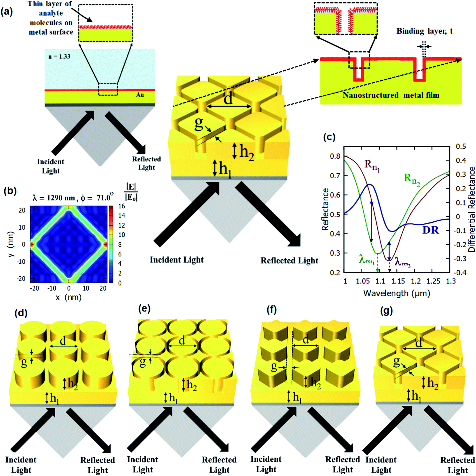 | ||
| Fig. 1 (a) Schematic of nanostructured plasmonic sensor chip, consisting of plasmonic nanostructures present on the surface of a plasmonic (Au) thin film, interrogated using the Kretschmann configuration with a 1 nm layer (red color) on top of the nanostructure. (b) xy-map of the E-field profile in the resonance condition for a nanostructured plasmonic thin film. (c) Differential reflectance spectra and reflectance spectra of a nanostructured plasmonic thin film in the presence and in the absence of the bio-layer. Schematic diagrams showing different configurations of the nanostructured plasmonic sensor chips: (d) a cylindrical nanopillar array, (e) a cylindrical nanoring hole array, (f) a diamond nanopillar array, and (g) a diamond nanoring hole array present on top of a 40 nm gold film and interrogated using the Kretschmann configuration. | ||
The sensitivity of plasmonic sensors is calculated as the shift in the resonance wavelength (or resonance angle) per unit change in the refractive index of the sensing medium. However, this definition is more suitable to define the bulk sensitivity (SB) of the sensors.15,37–40 In biomolecule detection, the change in the refractive index is highly localized to the surface of the plasmonic metal. Surface sensitivity (SS) is defined as the shift in the resonance wavelength (or resonance angle) per unit length of the bio-molecules attached to the plasmonic metal surface.37,38 The SPR sensors with higher bulk sensitivity can have lower surface sensitivity compared to LSPR sensors.
As the proposed nanostructured plasmonic sensors are suitable for spectral interrogation, the detection of biomolecules in spectral interrogation mode is accomplished by detecting the change in the plasmon resonance wavelength caused by a thin layer of biomolecules. Surface sensitivity (SS) is defined as the ratio of the wavelength shift in the plasmon resonance (ΔλS) caused by the biomolecules per unit length.37,38
 | (1) |
The localized sensor's figure of merit (FOMS) is defined as the ratio of the sensor's localized sensitivity to the full width half maximum (FWHM) of the associated plasmonic dip.37,38
 | (2) |
Furthermore, the sensitivity measurement in spectral interrogation or angular interrogation involves a complex optical setup and a spectrometer. A shift in the resonance wavelength or angle causes the change in the detected signal intensity at an incident angle and wavelength. This differential intensity signal at a single incident angle and wavelength can detect the change in the sensing medium refractive index instead of calculating the spectra or angular scanning.41–49 This method simplifies and miniaturizes the detection setup. Hence, in this paper, we have also used differential reflectance to quantify the sensitivity of the SPR sensors being proposed. Moreover, differential reflectance can also be useful for SPR imaging. The differential reflectance (DR) can be calculated as:
| DR(λ,ϕ) = Rn1(λ,ϕ) − Rn2(λ,ϕ) | (3) |
We should choose the optimized wavelength and incident angle for single point detection (single wavelength and incident angle) that shows the maximum sensitivity. The maximum differential reflectance (DRMax) can be defined as:
| DRMax = |DR(λ,ϕ)|Max | (4) |
Hence, along with employing surface sensitivity (SS) to quantify the changes in the spectra after binding of biomolecules, we also employ the maximum value of the differential reflectance (DRmax) as it is sometimes not easy to accurately determine the position of the plasmon resonance wavelengths or the shifts (ΔλS) in the plasmon resonance wavelengths, especially when the values of ΔλS are very small. On the other hand, it is not difficult to calculate the difference of the reflection spectra (DR) of the nanostructured SPR chip when a biomolecule layer is not present on its surface from the reflection spectra of the chip when a biomolecule layer is present on its surface. We can quantify this differential reflectance by determining the peak differential reflectance value, which is denoted as DRmax (as defined in eqn (4)). Differential reflectance can be employed effectively for SPR imaging as the difference of the spatial reflectance images can be obtained between the scenario when the biomolecule layer is present on the nanostructured SPR chip' surface and the scenario when the biomolecule layer is not present.
Hence, we have calculated the values of surface sensitivity (SS) and maximum differential reflectance (DRMax) to quantify the sensitivity performance of the sensor in this paper. We have presented four different nanostructured plasmonic sensing platforms for enhancement in the localized sensitivity. The thickness of the biomolecule layer above plasmonic metal is taken as 1 nm in our calculations. Moreover, the refractive index of the biomolecule layer is taken as 1.53 in our calculations based on the reports of the refractive indices of the nucleic acids being in the range from 1.46–1.55.50 More specifically, the refractive index of double stranded DNAs has been reported to be ∼1.53 for the visible spectral regime.50 So, the sensitivity is directly calculated in terms of surface sensitivity (SS) and maximum differential reflectance (DRMax) due to the change in the localized (1 nm above the metal film) refractive index from 1.33 to 1.53.
The standard Kretschmann configuration has been used to measure the sensitivity of the proposed nanostructured plasmonic sensor chips, as shown in Fig. 1(a). We have shown a very high surface sensitivity (SS) of 91 nm nm−1 in this work. This is the highest documented surface sensitivity value to date. We have also demonstrated a 500% enhancement in the maximum differential reflectance (DRmax)—which is also an indicator of the localized sensitivity of the SPR sensors43—over that of thin film-based localized SPR sensing. This is the highest reported improvement in the differential reflectance (by employing plasmonic micro- and nano-structures) reported over thin film-based SPR sensing. The surface sensitivity (SS) and FOMS of the nanostructured thin film presented in this paper are much greater than those previously reported. According to Table 1, the surface sensitivity of the suggested nanostructured thin film is 91 nm nm−1, which is more than the value reported in the prior literature. Additionally, the figure of merit of our suggested sensor is 0.59 nm−1, which is much greater than previously published values.
| Structure | S S (nm nm−1) | FOMS (nm−1) |
|---|---|---|
| a Calculated using eqn eqn (1) and (2). | ||
| Nanoellipsoid37 | ∼8 | 0.20 |
| Nanorings38 | 12 | 0.035 |
| Grating51 | ∼2.1a | ∼0.14a |
| Nanodisk array40 | ∼1.38a | ∼0.016a |
| Nanohole array52 | ∼2.5a | ∼0.33a |
| Fiber nanoprobe53 | ∼0.41a | ∼0.0028a |
| Gold-coated silver nanoprism54 | ∼6.67a | ∼0.046a |
| 3-Disk array55 | 6.06 | — |
| 2D plasmonic crystals56 | ∼1.67a | — |
| Nanogratings57 | ∼0.71a | — |
| Ring resonator arrays58 | ∼1.6 | ∼0.19 |
| Non-uniform nanogratings43 | 70 | 1.5 |
| Nanocrossess59 | 70 | 0.33 |
| This work | 91 | 0.59 |
The improvement in surface sensitivity (SS) and DRMax is achieved while using the traditional SPR systems based on Kretschmann configuration, and there is no requirement of a customized optical setup. The proposed sensor chips can be employed in conjunction with any Kretschmann configuration-based SPR or SPRi setup by just replacing the sensor chip with the chip containing the plasmonic nanostructures described in this paper. We study the effect of varying the different dimensional parameters of these arrays on the differential reflectance (DR). We numerically elucidate the optical response of a Kretschmann surface plasmon resonance sensor with these nanopillars and nanoring holes array structures for increased sensitivity. Hence, the detection of refractive index changes due to molecular binding events (such as antigen–antibody interactions) can be effectively monitored using the proposed nanostructured plasmonic sensor chips employed in the Kretschmann configuration, as shown in Fig. 1(a).
The proposed nanostructured plasmonic chips can be fabricated by using a combination of metal deposition techniques and conventional lithography. As a first step, gold can be deposited on a glass substrate using sputter deposition, employing an adhesion layer such as chromium or titanium. As extreme UV lithography can be employed to fabricate nanostructures below 7 nm,60,61 it can be employed to fabricate the proposed nanostructured plasmonic chips on top of the underlying gold layer on a wafer scale (6 inch, 12 inch, or 18 inch wafers). The proposed nanostructures can also be fabricated by first depositing a gold film on a glass substrate using sputter deposition, followed by focused ion beam (FIB) milling process58 or helium ion milling30,62 for patterning the top surface of the gold layer. We have to note that writing large areas using FIB milling or helium ion milling can not only be very a time consuming process but also very expensive. On the other hand, although extreme UV lithography equipment are very expensive, they are available these days with several commercial foundries that could be contracted for the fabrication of these nanostructured chips.
Rigorous coupled wave analysis simulations
We have simulated several different configurations of plasmonic nanostructures present on a plasmonic thin film—a cylindrical nanopillar array, a cylindrical nanoring array, a diamond nanopillar array, and a diamond nanoring array—in the Kretschmann configuration using commercial RSoft software using rigorous coupled wave analysis (RCWA). Fig. 1(d)–(g) shows the schematics of the structures being studied. An SF10 glass prism (np = 1.715) is used to couple surface plasmons on top of the nanostructured films. Different dimensional parameters are defined in Fig. 1. The number of harmonics is optimized to 6 in both x and y directions. The angulo-spectral reflectance maps for the proposed structures have been evaluated in the presence (Rn1) and absence (Rn2) of a 1 nm thick layer (nt = 1.53) for the incident p-polarised light. The medium above the nanostructures is taken as water (nd = 1.33).The incident angle is taken from 50° to 89°, and the incident light wavelength is taken in a range of 600–2000 nm. The angulo-spectral differential reflectance (DR) maps and maximum differential reflectance (DRMax) are calculated for each nanostructured film using eqn (1) and (2), respectively. The spectrum interrogation has been calculated at the incident angle of 75° for different nanostructured films. The surface sensitivity has been calculated from these reflectance spectra of different nanostructured films paper—both with the presence and with the absence of a biolayer on top of the nanostructures. The maximum differential reflectance (DRMax) and surface sensitivity (SS) have been optimized with different nanostructured films and their dimensions.
Results and discussion
The angulo-spectral reflectance maps are calculated for all the configurations of the nanostructured plasmonic sensor chips that are presented in this paper—both with the presence and with the absence of a biolayer on top of gold nanostructures. The corresponding differential reflectance (DR) angulo-spectral maps are also calculated using (1). Fig. 2 shows the reflectance spectra for all four configurations in the presence and absence of biolayer on top of gold nanostructures at different incident angles (ϕ). The DR spectra are also calculated and shown in Fig. 2 on secondary y-axes. The surface sensitivity (SS) is calculated directly from the shift in the plasmon resonance dips in the reflectance spectra due to the presence of the biolayer. The maximum differential reflectance (DRMax) is calculated from the DR spectra using (2). | ||
| Fig. 2 Reflectance and differential reflectance spectra of a: (a) cylindrical nanopillar array, (b) cylindrical nanoring hole array, (c) diamond nanopillar array, and (d) diamond nanoring hole array present on top of a 40 nm gold film and interrogated using the Kretschmann configuration. The reflectance spectra are calculated for both presence and absence of bio-layer. The values of h1 = 40 nm, h2 = 40 nm, d = 40 nm and g = 5 nm for all structures. | ||
We can observe from Fig. 2 that the plasmon resonance dips are deeper in diamond nanopillar and diamond nanoring hole arrays than cylindrical nanopillar and cylindrical nanoring hole arrays. Although, the diamond nanopillar arrays display a smaller shift (smaller SS) in plasmon resonance wavelength than the cylindrical nanopillar arrays. The shift in the plasmon resonance dips depends upon the high E-field values in the biolayer region. The larger regions of the high E-filed in the cylindrical nanopillar arrays result in a larger shift in the plasmon resonance dip compared to diamond nanopillar arrays (see Fig. 3). However, the diamond nanoring hole arrays display a larger shift (larger SS) in plasmon resonance wavelength than the cylindrical nanoring hole arrays. The larger regions of the high E-field in the diamond nanoring hole arrays result in a larger shift in the plasmon resonance dip compared to cylindrical nanoring hole arrays (see Fig. 3).
 | ||
| Fig. 3 E-field profiles for a cylindrical nanopillar array present on top of a 40 nm gold film and interrogated using the Kretschmann configuration calculated for: (a) on-resonance condition and (b) off-resonance condition. E-field profiles for a cylindrical nanoring hole array present on top of a 40 nm gold film calculated for: (c) on-resonance condition and (d) off-resonance condition. E-field profiles for a diamond nanopillar array present on top of a 40 nm gold film calculated for: (e) on-resonance condition and (f) off-resonance condition. E-field profiles for a diamond nanoring hole array present on top of a 40 nm gold film calculated for: (g) on-resonance condition and (h) off-resonance condition. The values of h1 = 40 nm, h2 = 40 nm, d = 40 nm, and g = 5 nm for all structures. | ||
We can also observe from Fig. 2 that the values of DRMax are very close to each other for the cylindrical and the diamond nanopillar arrays. The cylindrical nanopillar arrays have a smaller E-field enhancement but a larger region of high E-field enhancement than in the diamond nanopillar arrays. Hence the effect of high E-field enhancement in diamond pillar arrays is compensated by the reduced region of the high E-field. The DRMax is very high in the diamond nanoring hole arrays as compared to the cylindrical nanoring hole arrays. This is due to the high E-field enhancements and the larger region of high E-field present in diamond nanoring hole arrays than in the cylindrical nanoring hole arrays.
The E-field profiles of the four nanostructures for on-resonance and off-resonance cases are shown in Fig. 3. The comparison between on-resonance and off-resonance clearly shows the high electric field regions are present in the on-resonance condition. The plasmon resonance wavelengths and the incident angles are written on top of each E-field profile. The E-field enhancement is higher in the diamond nanopillars and in the nanoring hole arrays than in the other two nanostructures. The higher electric field is present near two corners of the diamond nanopillars as smaller corners of the diamond nanopillars enhance the electric field more.63
Fig. 4 shows the angulo-spectral reflectance maps of the nanostructured chips in the presence and absence of biolayer on top of the structures. The corresponding angulo-spectral DR maps are also calculated. We can observe from Fig. 4 that the plasmon resonance dips shift to a larger wavelength and a higher incident angle in the presence of the bio-layer as the bio-layer increases the refractive index in the vicinity of the gold surface. This modifies the effective permittivity εeff on top of the gold surface and shifts the plasmon resonance wavelengths and incident angles.5,64,65 The shift in the plasmon resonance wavelengths and incident angles results in the change in the reflectance signal shown in DR angulo-spectral maps. The interaction of SPR with the gold nanostructures on top of the gold film modifies the plasmon dips in the angulo-spectral maps.
 | ||
| Fig. 4 Angulo-spectral reflectance (without biolayer in column 1 (a1–d1) and with biolayer in column 2 (a2–d2)) and differential reflectance (column 3 (a3–d3)) maps of the proposed nanostructured chips (a1–a3) cylindrical nanopillar array, (b1–b3) diamond nanopillar array, (c1–c3) cylindrical nanoring hole array, and (d1–d3) diamond nanoring hole array. The values of h1 = 40 nm, h2 = 40 nm and g = 5 nm for all structures. The values of d for cylindrical nanopillar array, diamond nanopillar array, cylindrical nanoring hole array and diamond nanoring hole array are 60 nm, 40 nm, 60 nm, and 40 nm, respectively. Schematics of the nanopillar arrays present on top of gold films are shown in column 4. | ||
The nanostructured films could be considered as two films of thicknesses h1 and (h1 + h2) for SPR coupling. As the thickness of the gold film increases in the Kretschmann configuration, the plasmon dips shift towards the larger wavelengths and incident angles.66–68 The surface area of the top of the nanopillars in the case of the cylindrical nanopillar arrays is larger than in the case of the diamond nanopillar array. So, in the cylindrical nanopillar arrays, the top film (thickness = h1 + h2) has larger share of the SPR coupling than in the diamond nanopillar arrays. Hence, in the case of the cylindrical nanopillar arrays, the plasmon resonance dips are red-shifted further than in the case of the diamond nanopillar arrays (see Fig. 4(a1) and (b1)). The DRMax is almost the same for the cylindrical and the diamond nanopillar arrays as explained earlier and can be observed from Fig. 4(a3) and (b3).
The surface area of the top of the nanoring hole arrays are larger than the nanopillar arrays. So, in the nanoring hole arrays, the top film (thickness = h1 + h2) has a larger share of the SPR coupling than in the nanopillar arrays. Hence, in the case of nanoring hole arrays, the plasmon resonance wavelengths shift more than in the nanopillar arrays (see Fig. 4). The DRMax is higher for diamond nanoring hole arrays than in other structures, as explained earlier, and can be observed in Fig. 4(c3) and (d3).
Fig. 5 shows the effect of variation in parameter ‘g’ of four nanostructures presented on the SS and DRMax. A decrease in the value of parameter ‘g’ increases the values of SS and DRMax both in all the four structures presented. As parameter ‘g’ decreases, it reduces the gap between the two adjacent nanopillars. This increases the near-field coupling between the gold nanopillars and reduces the far-field scattering.5 Hence, a strong E-field is localized inside the gap between the nanopillars or inside nanoring holes, and it increases with the decrease in the spacing between adjacent nanopillars. Hence, the smaller values of ‘g’, enhance the E-field around the nanopillars and inside the nanoring holes. This enhanced E-field increases the shift in the plasmon resonance wavelengths and incident angles in the presence of a bio-layer. Hence, a smaller value of ‘g’ increases the values of SS and DRMax. The FOMS values for the four nanostructured thin films with varying values of the parameter ‘g’ were also calculated and are listed in ESI Table S1.† It can be observed that the FOMS values follow the trend of surface sensitivity (SS) values.
 | ||
| Fig. 5 Effect of variation in parameter ‘g’ on the values of the surface sensitivity (SS) and maximum differential reflectance (DRMax) for different configurations of the nanostructures present on top of a thin gold film: (a) and (c) A cylindrical nanopillar array and a diamond nanopillar array and (b) and (d) a cylindrical nanoring hole array and a diamond nanoring hole array. For comparison, the maximum differential reflectance for an optimized plain gold film is also shown in the figures with a dashed line. The values of both h2 and d are taken as 40 nm. | ||
The effect of variation in parameter ‘h2’ of four nanostructures presented on the values of SS and DRMax are enclosed in the ESI.† An increase in the value of parameter ‘h2’ increases the values of SS and DRMax initially and then reduces it for all the four structures presented. The increase in the values of ‘h2’ increases the volume of nanopillars and nanoring holes above the gold film. This increases the regions of high E-field alongside the wall of the nanopillars or in the depth of the nanoring holes. The increase in the high E-field regions increases the shift in the plasmon resonance wavelength and hence increases the values of SS and DRMax. However, a higher value of ‘h2’ also reduces the probability of coupling surface plasmons on top of the nanopillars or top surface of the nanoring holes as the evanescent tail of the plasmon will no longer be able to reach the top surface. This reduces the values of SS and DRMax with a further increase in the value of ‘h2’. The FOMS values for the four nanostructured thin films with varying values of the parameter ‘h2’ were also calculated and are listed in ESI Table S2.† Similar to surface sensitivity, the FOMS values reach a maximum at some optimal value of h2.
The plain gold film in Kretschmann configuration provides a 3 nm nm−1 of SS for 56 nm of gold film on SF10 glass prism (np = 1.715) at 75° of incident angle. The proposed cylindrical nanoring hole array shows a 25-fold improvement in the value of SS (76 nm nm−1) for d = 50 nm, h2 = 45 nm, and g = 5 nm. The other structures also show a substantial improvement in SS values for different values of parameters. The value SS for diamond nanoring hole array is calculated to be 60 nm nm−1, for cylindrical nanopillar array is calculated to be 37 nm nm−1, and for diamond nanopillar array is calculated to be 26 nm nm−1 for d = 50 nm, g = 5 nm, h2 = 70 nm (see Fig. S1 in ESI†).
The plain gold film in Kretschmann configuration—optimized for a higher value of DRMax—provides a 9.13% of DRMax for 56 nm of gold film on SF10 glass prism (np = 1.715). The proposed cylindrical nanoring hole array shows a five-fold improvement in the value of DRMax (46%) for d = 40 nm, h2 = 40 nm, and g = 5 nm. The other structures also show a substantial improvement in DRMax values for different values of parameters. The DRMax for diamond nanoring hole array is calculated to be 34% for d = 50 nm, g = 5 nm, h2 = 70 nm. For cylindrical nanopillar array, DRMax of 25% is noted for d = 50 nm, g = 5 nm, h2 = 30 nm. For diamond nanopillar array, DRMax of 28% is noted for d = 40 nm, g = 5 nm, h2 = 40 nm.
By varying the aspect ratio (r = dy/dx) of the nanopillars or nanoring holes, the sensitivity is increased even further. The aspect ratio of 2 has been estimated to have the highest SS and DRMax for diamond nanoring hole array. For diamond nanoring hole array with r = 2, d = 50 nm, h2 = 40 nm, and g = 5 nm, the optimal surface sensitivity (SS) and DRMax are calculated to be 91 nm nm−1 and 55%, respectively. Additionally, the optimized FOMS value was determined to be 0.59 nm−1 for a diamond nanoring hole array having r = 2, d = 50 nm, h2 = 40 nm, and g = 5 nm.
When considering an experimental system for detecting the intensity change in an SPR or SPRi setup, the practically realizable values of DRMax could be lower due to the non-uniform concentration of biomolecules on the nanostructured films. However, it is worth mentioning that the substantially high values of numerically evaluated DRMax in this work are achieved for a relatively small thickness of a biomolecular binding layer of 1 nm, while in an actual experimental system, the biomolecular binding layer is generally of a larger thickness which could result in even higher values of practically realizable DRMax values for the proposed nanostructured thin film sensing platforms, thus confirming the robustness of the proposed sensing platforms. To the best of the authors' knowledge, such large values of SS and DRMax have not been reported till now. The high value of SS and DRMax could also be achieved at a desired operating wavelength and angle of incidence (within an acceptable range) by engineering the different parameters of the nanostructures. This provides the tunability of the sensor from visible to near IR regime. As the sensor has also been studied using the sensing parameter DRMax, these sensors can directly be used in SPR imaging (SPRi) with high contrast in the sensing images.
Conclusion
We have presented four different configurations of nanostructured plasmonic sensor chips based on a combination of both propagating surface plasmons as well as localized surface plasmons for the highly sensitive detection of biomolecules. As the proposed sensors work in the Kretschmann configuration, they can be implemented on the optical setups used for the conventional Kretschmann configuration-based sensors. The proposed sensors could be implemented either using spectral interrogation (at a fixed angle of incidence) or using angular interrogation (at a fixed wavelength). We show their implementation using the measurement of the surface sensitivity (SS) at a fixed incident angle. We also show their implementation using maximum differential reflectance (DRMax) at a fixed wavelength and a fixed incident angle—which alleviates the need for spectral or angular scanning, and can lead to simplification and miniaturization of the detection setup. We varied the structural parameters of the different plasmonic sensor configurations to maximize the values of the surface sensitivity (SS) and the maximum differential reflectance (DRMax). As the sensor is based on the detection of the changes in the reflected intensity signal, it can easily be used in SPRi setups. We demonstrate a 30-fold improvement in the surface sensitivity (SS) and a six-fold improvement in the maximum differential reflectance (DRMax) over that of thin film-based SPR sensing. Extremely high values of surface sensitivity and FOMS of 91 nm nm−1 and 0.59 nm−1 have been demonstrated, respectively, for one of the proposed nanostructured sensing platforms containing diamond nanoring hole array structures. It has been shown that the dimensions of the nanostructures can be varied to tune the operational wavelength and incident angle. The sensor shows a high tunability of operation from the visible spectral region to the near IR region, with the incident angle ranging from 55° to 89°.Conflicts of interest
There are no conflicts to declare.Acknowledgements
Above all, A. D. would like to thank Lord Jesus Christ for blessing this work. A. D. would also like to thank the Digital India Corporation. This work was supported in part by the Defence Research and Development Organization (RP03436G, RP03356G, RP03437G), Ministry of Human Resource Development (RP03417G, RP03246G), and SERB (RP03932G).References
- P. Guedon, T. Livache, F. Martin, F. Lesbre, A. Roget, G. Bidan and Y. Levy, Anal. Chem., 2000, 72, 6003–6009 CrossRef CAS PubMed.
- B. P. Nelson, T. E. Grimsrud, M. R. Liles, R. M. Goodman and R. M. Corn, Anal. Chem., 2001, 73, 1–7 CrossRef CAS PubMed.
- J. Homola, Chem. Rev., 2008, 108, 462–493 CrossRef CAS PubMed.
- W. L. Barnes, A. Dereux and T. W. Ebbesen, Nature, 2003, 424, 824–830 CrossRef CAS PubMed.
- S. A. Maier, Plasmonics: Fundamentals and Applications, Springer, New York, USA, 2007, vol. 677 Search PubMed.
- J. Homola, Anal. Bioanal. Chem., 2003, 377, 528–539 CrossRef CAS PubMed.
- W. Kong, Z. Zheng, Y. Wan, S. Li and J. Liu, Sens. Actuators, B, 2014, 193, 467–471 CrossRef CAS.
- C.-T. Li, T.-J. Yen and H. Chen, Opt. Express, 2009, 17, 20771 CrossRef CAS PubMed.
- A. Kumar, A. K. Yadav, A. S. Kushwaha and S. K. Srivastava, Sensors and Actuators Reports, 2020, 2, 100015 CrossRef.
- M. Chamtouri, A. Dhawan, M. Besbes, J. Moreau, H. Ghalila, T. Vo-Dinh and M. Canva, Plasmonics, 2014, 9, 79–92 CrossRef CAS.
- K. Kim, S. J. Yoon and D. Kim, Opt. Express, 2006, 14, 12419 CrossRef PubMed.
- P. Arora, E. Talker, N. Mazurski and U. Levy, Sci. Rep., 2018, 8, 9060 CrossRef PubMed.
- A. Shalabney, C. Khare, B. Rauschenbach and I. Abdulhalim, Sens. Actuators, B, 2011, 159, 201–212 CrossRef CAS.
- A. K. Agrawal, S. Yadav and A. Dhawan, in 2018 IEEE 18th International Conference on Nanotechnology (IEEE-NANO), IEEE, Cork, Ireland, 2018, pp. 1–4 Search PubMed.
- S. Roh, T. Chung and B. Lee, Sensors, 2011, 11, 1565–1588 CrossRef PubMed.
- H. J. Lee, A. W. Wark and R. M. Corn, Langmuir, 2006, 22, 5241–5250 CrossRef CAS PubMed.
- L. K. Wolf, D. E. Fullenkamp and R. M. Georgiadis, J. Am. Chem. Soc., 2005, 17453–17459 CrossRef CAS PubMed.
- V. Kanda, P. Kitov, D. R. Bundle and M. T. Mcdermott, Anal. Chem., 2005, 77, 7497–7504 CrossRef CAS PubMed.
- M. Kyo, K. Usui-aoki and H. Koga, Anal. Chem., 2005, 77, 7115–7121 CrossRef CAS PubMed.
- M. Kyo, T. Yamamoto, H. Motohashi, T. Kamiya and T. Kuroita, Genes Cells, 2004, 9, 153–164 CrossRef CAS PubMed.
- G. J. Wegner, A. W. Wark, H. J. Lee, E. Codner, T. Saeki, S. Fang and R. M. Corn, Anal. Chem., 2004, 76, 5677–5684 CrossRef CAS PubMed.
- V. Kanda, J. K. Kariuki, D. J. Harrison and M. T. Mcdermott, Anal. Chem., 2004, 76, 7257–7262 CrossRef CAS PubMed.
- J. S. Shumaker-parry, M. H. Zareie, R. Aebersold and C. T. Campbell, Anal. Chem., 2004, 76, 918–929 CrossRef CAS PubMed.
- G. J. Wegner, H. J. Lee, G. Marriott and R. M. Corn, Anal. Chem., 2003, 75, 4740–4746 CrossRef CAS PubMed.
- E. A. Smith, M. G. Erickson, A. T. Ulijasz, B. Weisblum and R. M. Corn, Langmuir, 2003, 19, 1486–1492 CrossRef CAS.
- G. J. Wegner, H. J. Lee and R. M. Corn, Anal. Chem., 2002, 74, 5161–5168 CrossRef CAS PubMed.
- A. W. Wark, H. J. Lee and R. M. Corn, Advanced Methods for SPR Biosensing, in Handbook of Surface Plasmon Resonance, ed. R. B. M. Schasfoort and A. J Tudos, RSC Publishing, 2008, pp. 251–280, ISBN: 978-0-85404-267-8 Search PubMed.
- T. T. Goodrich, H. J. Lee and R. M. Corn, J. Am. Chem. Soc., 2004, 126, 4086–4087 CrossRef CAS PubMed.
- T. T. Goodrich, H. J. Lee and R. M. Corn, Anal. Chem., 2004, 76, 6173–6178 CrossRef CAS PubMed.
- L. A. Lyon, M. D. Musick and M. J. Natan, Anal. Chem., 1998, 70, 5177–5183 CrossRef CAS PubMed.
- L. He, M. D. Musick, S. R. Nicewarner, F. G. Salinas, S. J. Benkovic, M. J. Natan and C. D. Keating, J. Am. Chem. Soc., 2000, 122, 9071–9077 CrossRef CAS.
- S. Fang, H. J. Lee, A. W. Wark and R. M. Corn, J. Am. Chem. Soc., 2006, 128, 14044–14046 CrossRef CAS PubMed.
- L. Malic, B. Cui, T. Veres and M. Tabrizian, Opt. Lett., 2007, 32, 3092 CrossRef CAS PubMed.
- L. S. Live, J. Breault-turcot, K. Nguyen, J. Masson, U. De Montréal and C. P. S. Centre-ville, in Plasmonics in Biology and Medicine VIII, San Francisco, California, United States, 2011, vol. 7911, pp. 3–9 Search PubMed.
- L. S. Live, O. R. Bolduc and J. Masson, Anal. Chem., 2010, 82, 3780–3787 CrossRef CAS PubMed.
- L. S. Live, A. Dhawan, K. F. Gibson, M. Canva, T. Vo-dinh and J. Masson, Anal. Bioanal. Chem., 2012, 404, 2859–2868 CrossRef CAS PubMed.
- M. A. Otte, B. Sepúlveda, W. Ni, J. P. Juste, L. M. Liz-Marzán and L. M. Lechuga, ACS Nano, 2010, 4, 349–357 CrossRef CAS PubMed.
- H. Jiang and J. Sabarinathan, J. Phys. Chem. C, 2010, 114, 15243–15250 CrossRef CAS.
- J. Homola, S. Y. Yee and G. Gauglitz, Sens. Actuators, B, 1999, 54, 3–15 CrossRef CAS.
- Y. Liang, W. Cui, L. Li, Z. Yu, W. Peng and T. Xu, Adv. Opt. Mater., 2019, 7, 1801269 CrossRef.
- Y. Sharma, V. A. Tiruveedhula, J. F. Muth and A. Dhawan, Opt. Express, 2015, 23, 5822 CrossRef CAS PubMed.
- A. Dhawan, M. Canva and T. Vo-Dinh, Opt. Express, 2011, 19, 787 CrossRef CAS PubMed.
- A. K. Agrawal, A. Suchitta and A. Dhawan, IEEE Access, 2021, 9, 10136–10152 Search PubMed.
- Y. Wang, L. Zhang, C. Su, H. Xiao, S. Lv, F. Zhang, Q. Sui, L. Jia and M. Jiang, Nanomaterials, 2019, 9, 1640 CrossRef CAS PubMed.
- R. Forker, M. Gruenewald and T. Fritz, Annu. Rep. Prog. Chem., Sect. C: Phys. Chem., 2012, 108, 34–68 RSC.
- M. Piliarik, H. Vaisocherová and J. Homola, Biosens. Bioelectron., 2005, 20, 2104–2110 CrossRef CAS PubMed.
- X. Ma, X. Xu, Z. Zheng, K. Wang, Y. Su, J. Fan, R. Zhang, L. Song, Z. Wang and J. Zhu, Sens. Actuators, A, 2010, 157, 9–14 CrossRef CAS.
- J. Wu, Y. Huang, X. Bian, D. Li, Q. Cheng and S. Ding, Opt. Commun., 2016, 377, 24–32 CrossRef CAS.
- J. C. Yang, J. Ji, J. M. Hogle and D. N. Larson, Biosens. Bioelectron., 2009, 24, 2334–2338 CrossRef CAS PubMed.
- S. Elhadj, G. Singh and R. F. Saraf, Langmuir, 2004, 20, 5539–5543 CrossRef CAS PubMed.
- J. Li, J. Ye, C. Chen, Y. Li, N. Verellen, V. V. Moshchalkov, L. Lagae, P. Van Dorpe, P. Van Dorpe and P. Van Dorpe, ACS Photonics, 2015, 2, 425–431 CrossRef CAS.
- M. Vala, C. T. Ertsgaard, N. J. Wittenberg and S. H. Oh, ACS Sens., 2019, 4, 3265–3274 CrossRef CAS PubMed.
- Y. Liang, Z. Yu, L. Li and T. Xu, Sci. Rep., 2019, 9, 1–7 CrossRef PubMed.
- E. Martinsson, M. M. Shahjamali, K. Enander, F. Boey, C. Xue, D. Aili and B. Liedberg, J. Phys. Chem. C, 2013, 117, 23148–23154 CrossRef CAS.
- L. Y. M. Tobing, A. M. Soehartono, A. D. Mueller, K. T. Yong, W. Fan and D. H. Zhang, Nanoscale, 2021, 13, 4092–4102 RSC.
- H. Gao, J. C. Yang, J. Y. Lin, A. D. Stuparu, M. H. Lee, M. Mrksich and T. W. Odom, Nano Lett., 2010, 10, 2549–2554 CrossRef CAS PubMed.
- S. Savoia, A. Ricciardi, A. Crescitelli, C. Granata, E. Esposito, V. Galdi and A. Cusano, Opt. Express, 2013, 21, 23531 CrossRef CAS PubMed.
- J. Lee, S. Sung, J. H. Choi, S. C. Eom, N. A. Mortensen and J. H. Shin, Sci. Rep., 2016, 6, 1–8 CrossRef CAS PubMed.
- A. Das, K. Kumar and A. Dhawan, RSC Adv., 2021, 11, 8096–8106 RSC.
- L. Li, X. Liu, S. Pal, S. Wang, C. K. Ober and E. P. Giannelis, Chem. Soc. Rev., 2017, 46, 4855–4866 RSC.
- B. Wu and A. Kumar, J. Vac. Sci. Technol., B: Microelectron. Nanometer Struct., 2007, 25, 1743 CrossRef CAS.
- H. Kollmann, X. Piao, M. Esmann, S. F. Becker, D. Hou, C. Huynh, L. O. Kautschor, G. Bösker, H. Vieker, A. Beyer, A. Gölzhäuser, N. Park, R. Vogelgesang, M. Silies and C. Lienau, Nano Lett., 2014, 14, 4778–4784 CrossRef CAS PubMed.
- M. Urbieta, M. Barbry, Y. Zhang, P. Koval, D. Sánchez-Portal, N. Zabala and J. Aizpurua, ACS Nano, 2018, 12, 585–595 CrossRef CAS PubMed.
- M. Piliarik and J. Homola, Opt. Express, 2009, 17, 16505–16517 CrossRef CAS PubMed.
- J. Homola, Sens. Actuators, B, 1997, 41, 207–211 CrossRef CAS.
- H. S. Leong, J. Guo, R. G. Lindquist and Q. H. Liu, J. Appl. Phys., 2009, 106, 124314 CrossRef.
- K. J. Kasunic, Appl. Opt., 2000, 39, 61 CrossRef CAS PubMed.
- J. Heckmann, K. Pufahl, P. Franz, N. B. Grosse, X. Li and U. Woggon, Phys. Rev. B, 2018, 98, 1–8 CrossRef.
Footnotes |
| † Electronic supplementary information (ESI) available. See DOI: 10.1039/d1ra07937a |
| ‡ Both authors contributed equally to this work. |
| This journal is © The Royal Society of Chemistry 2022 |