
 Open Access Article
 This Open Access Article is licensed under a Creative Commons Attribution-Non Commercial 3.0 Unported Licence
Investigation of correlative parameters to evaluate EUV lithographic performance of PMMA
Kanghyun Kim†
ab,
Jong-Won Lee† b,
Byeong-Gyu Parkb,
Hyun-Taek Ohc,
Yejin Kud,
Jin-Kyun Leecd,
Geunbae Lim*a and
Sangsul Lee*b
b,
Byeong-Gyu Parkb,
Hyun-Taek Ohc,
Yejin Kud,
Jin-Kyun Leecd,
Geunbae Lim*a and
Sangsul Lee*b
aDepartment of Mechanical Engineering, POSTECH, Pohang, 37673, Republic of Korea
bPohang Accelerator Laboratory, POSTECH, Pohang, 37673, Republic of Korea. E-mail: sangsul@postech.ac.kr
cDepartment of Polymer Engineering, Inha University, Incheon 22212, Republic of Korea
dProgram in Environmental and Polymer Engineering, Inha University, Incheon 22212, Republic of Korea
First published on 19th January 2022
Abstract
Investigations to evaluate the extreme ultraviolet (EUV) lithographic performance of 160 nm thick poly(methyl methacrylate) with 13.5 nm wavelength EUV light were performed using a synchrotron radiation source at Pohang Light Source-II (PLS-II). The single system enabled the determination of the sensitivity, contrast, linear absorption coefficient, critical dimension, and line edge roughness of polymer thin films through tests and measurements. The experimental findings were also compared to theoretical results and those of previously reported studies. According to the results of the dose-to-clear test and transmission measurements, the critical dimension of a line and space pattern (>50 nm) via interference lithography with 250 nm pitch grating agreed well with the results calculated using the lumped parameter model. The experimental results demonstrated that the equipment and test protocol can be used for EUV material infrastructure evaluation in academia and in industry.
1. Introduction
Lithography and inspection using extreme ultraviolet (EUV) light are crucial steps for the fabrication of highly integrated semiconductor chips in accordance with Moore's law, wherein the performance of semiconductors doubles approximately every two years.1–3 In the semiconductor industry and in leading research laboratories, EUV patterning technologies have been studied for advanced processes and applications, such as development of 20 nm period line/space patterns as well as adaption of high numerical aperture optics.4,5 In addition, for studies on key components, such as photoresists, photomasks, and pellicles, synchrotron-radiation-based EUV sources have been widely employed as experimental platforms. For instance, the Swiss Light Source provides resist patterning tools for periodic nanostructure fabrication.6 In addition, an actinic mask inspection system was implemented.3 The Advanced Light Source developed a projection exposure tool with a numerical aperture of 0.5 (i.e., the MET-5) for high-resolution printing.7 The New SUBARU provides a platform to study the optical properties of components employed for EUV lithography processes.8According to specific targets and demands, different lithographic tools employing several sources, including electron beam and EUV light, have been used to the exposure processes of the resist materials. Based on a highly focused beam, lithography via highly energetic electrons is generally used to print high-resolution patterns.9 By contrast, photon-based lithography is widely applied for mass production at a high repetition rate.10 In aspect of physical mechanism, electron source directly induces bonding scission and/or cross-link. In photon source, the ionization process exciting bound electrons becomes crucial.11,12 Moreover, this process is governed by the wavelength of light. Therefore, the lithographic performance depending on exposure tool must be studied.13–15 For instance, sensitivity, defined as the exposure energy at half residual film thickness, can be utilised to determine the required throughput of the lithographic tool.16,17 The contrast, defined as the slope of transition between light and dark areas, relates to critical dimension (CD, i.e. pattern resolution) control.18 These properties directly contribute to the lithographic patterning performance, e.g. CD, line edge roughness (LER), and Resolution-Line Edge Roughness–Sensitivity (RLS) properties.6 In particular, the evaluation of these lithographic parameters is essential for the discovery of novel photoresists and optimization of their performance for application in EUV lithography. For instance, elucidation of the mechanism of the photon–resist interaction,19 characterization of the chemical compound,20 and configuration of molecular density of photoresists21 are critical for directly improving the performance of electronic devices, such as MOSFETs22 and FinFETs.23
This paper reports a comprehensive study for evaluating the EUV lithographic performance of poly(methyl methacrylate) (PMMA) films with correlative parameters. Measurements were performed using a single instrumentation supplied at the Pohang Light Source-II (PLS-II) of the Pohang Acceleration Laboratory. In a single experimental station, three tests/measurements, including the dose-to-clear test (DCT), EUV transmission measurements, and two-slit interference lithography (IL), were performed by simply changing the components. PMMA films were used as test resists. In the DCT, the sensitivity and contrast of a 160 nm thick PMMA film were determined on the basis of a fit with the dose–response function. To determine the lithographic resolution (i.e. CD) experimentally, the obtained results were compared with those of previous studies and those obtained by calculations using the lumped parameter model (LPM).14 In addition, the linear absorption coefficient, which can be used in the LPM, was experimentally measured. This study can facilitate the development of novel techniques for EUV lithography and promote the research on the characteristics of photoresists.
2. Experimental setup
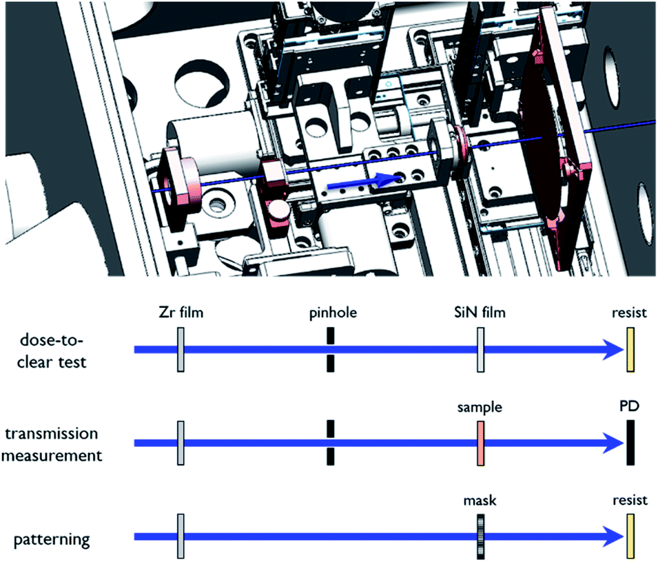
An experimental system was constructed, and the experiments were conducted at the 4A1 beamline (4A1 BL) of PLS-II. PLS-II was operated at an electron energy of 3 GeV, a current of 250 mA, and a repetition rate of 500 MHz. The photon energy range of this beamline ranges from 30 to 1000 eV, based on an elliptically polarizing undulator with 11.4 cm period. Owing to the horizontal focusing mirror, the beam was focused onto the exit slit. The vertical focusing mirror focused the beam onto the entrance slit. A monochromatic beam was obtained using six spherical grating mirrors.Fig. 1 shows the experimental chamber used to evaluate the EUV lithographic performance. The system was installed 32.11 m downstream from the undulator. The components at specific positions were changed according to the measurement requirements. In all measurements, Zr films were used to attenuate the EUV photons. The series of attenuators consisted of 200–1000 nm thick Zr films. The corresponding attenuation ranged between 0.5 and 10−2. In addition, this component removed scattered and frequency-doubled/tripled light from the main beam. The spectral properties of the EUV beam remained unaffected because the bandwidth, which is narrower than the spectral regime of the highly transmitting Zr film, was mainly controlled by the monochromator system. For the DCT and transmission measurements, a set of pinholes with aperture diameters of 50–500 μm was used to control the irradiated and measured areas. In the DCT, the photon number could be precisely controlled from 5% to 50% by using additional attenuators consisting of 100–300 nm thick Si3N4 membranes. This essential component afforded a low dose, which could not be achieved by using the shutter. Finally, a circular beam irradiated the resist. In the transmission measurement, 15 samples with an effective area of 3 × 3 mm2 could be loaded. The transmitted beam signal was digitalized by an EUV photodiode (Optodiode, AXUV 100G) and an electrometer (Keithley, model 6514).
 | ||
| Fig. 1 Schematic of the experimental system and measurements. In the upper panel, the key components are highlighted. | ||
In the patterning test, a two-slit grating mask was located 0.77 m downstream from the horizontal exit slit in the monochromator system. As shown in Fig. 2, the spacing between both apertures is 20 μm, and the size of each aperture is 100 × 20 μm2. The 20 nm thick Cr grating on the Si3N4 membrane consists of 40 lines with a 500 nm period; the line is 230 nm wide. To improve the diffraction efficiency, the etched Si3N4 membrane between the gratings was 70 nm thick. The resulting diffraction efficiency for each grating, calculated through the rigorous coupled-wave analysis, was 4.0%.24 The light of the EUV beam that passed outside the grating was blocked by the photoresist beam stop, which was supplied by Eulitha.25 The distance between the mask and wafer was set according to the depth-of-focus of the grating. All tests and measurements were performed at 0.2% EUV energy fluctuations of 4 × 10⁻⁷ torr under the ultra-high vacuum condition.
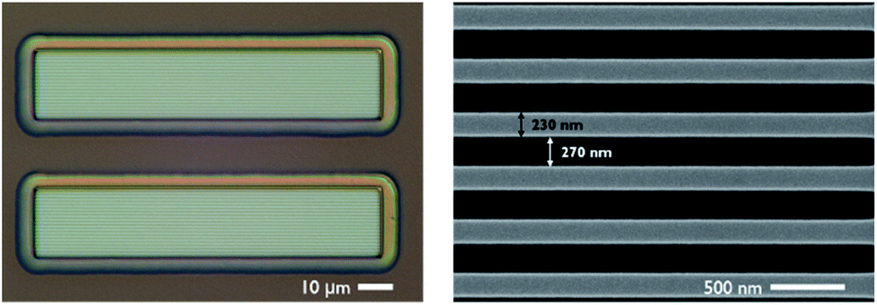 | ||
| Fig. 2 (Left) microscopy and (right) SEM images of the two-slit mask. | ||
The photon energy bandwidth of the EUV beam used for lithography was estimated through high-resolution photoemission spectroscopy and by using a clean gold surface. The 6s electron band that intersects with the Fermi level had the Fermi–Dirac distribution; the broadening width of the step of the Fermi–Dirac distribution was proportional to the photon resolution of the EUV source. This broadening section was estimated as the full width at half maximum (FWHM) of the 6s band spectrum through HRPES. The measured FWHM value of 600 μm vertical exit slit was 342 meV, corresponding the EUV bandwidths was 0.37%. Utilizing narrow bandwidth is the most advantage of synchrotron-based EUV source. Otherwise, the laser-produced plasma source typically provides a bandwidth of 2–4% by using EUV optics and/or spectral filter.26 The EUV beam profile was captured via pinhole scanning. The result was obtained by deconvolution with respect to the aperture size of the pinhole (25 μm). The FWHM beam diameters in the vertical and horizontal directions were 0.80 and 0.58 mm, respectively. Because of the large diameter, the region that overlaps with the apertures of the two-slit mask is approximately a flat top. The root mean square deviation of the EUV energy, averaged over the two-slit mask, was less than 0.5%.
3. Results and discussion
3.1. DCT
To test the EUV photon–resist interaction, PMMA was explored using the DCT. To apply the photoresist film, a PMMA solution in a chlorobenzene solvent (Kayaku, 950 PMMA C2) was coated on a 4 inch and 525 μm thick Si (100) substrate. The spin-coating process was performed at 750 rpm for 60 s. The thickness of the resulting PMMA film was measured to be 160 nm using an Alpha-Step profiler. Post application bake (PAB) was performed at 180 °C for 60 s. After EUV exposure, the sample was developed in a mixture of methyl isobutyl ketone (MIBK) and isopropyl alcohol (IPA) at a ratio of 1![[thin space (1/6-em)]](https://www.rsc.org/images/entities/char_2009.gif) :3 and rinsed in deionised water for 30 s. The EUV beam size was reduced by a 450 μm diameter pinhole; because of the aperture size, the diffraction patterns could be neglected in the analysis. During exposure, the EUV light caused the main chain and side chain scission of PMMA (i.e. the single carbon bonds of PMMA are destroyed). Side chain scission generated methyl formate, which promotes the main chain scission.27 The degraded PMMA film was dissolved in the developer. The remaining thickness was measured with a three-dimensional optical profiler (Bruker, ContourX-100), which is typically used to visualize the surface as a metrology tool. Fig. 3 shows the dose-dependent normalized thickness of the 160 nm thick PMMA film. Herein, this sample thickness was primarily employed for a comprehensive study. Error bars represent the standard deviation of the remaining thickness of the irradiated areas. The errors might be affected by the cleanliness of the PMMA surface after exposure and development. In addition, because the remaining thickness decreased, the error of the measurement tool can be remarkably increased, owing to the intensity of the probe beam that is reflected by the Si substrate.
:3 and rinsed in deionised water for 30 s. The EUV beam size was reduced by a 450 μm diameter pinhole; because of the aperture size, the diffraction patterns could be neglected in the analysis. During exposure, the EUV light caused the main chain and side chain scission of PMMA (i.e. the single carbon bonds of PMMA are destroyed). Side chain scission generated methyl formate, which promotes the main chain scission.27 The degraded PMMA film was dissolved in the developer. The remaining thickness was measured with a three-dimensional optical profiler (Bruker, ContourX-100), which is typically used to visualize the surface as a metrology tool. Fig. 3 shows the dose-dependent normalized thickness of the 160 nm thick PMMA film. Herein, this sample thickness was primarily employed for a comprehensive study. Error bars represent the standard deviation of the remaining thickness of the irradiated areas. The errors might be affected by the cleanliness of the PMMA surface after exposure and development. In addition, because the remaining thickness decreased, the error of the measurement tool can be remarkably increased, owing to the intensity of the probe beam that is reflected by the Si substrate.
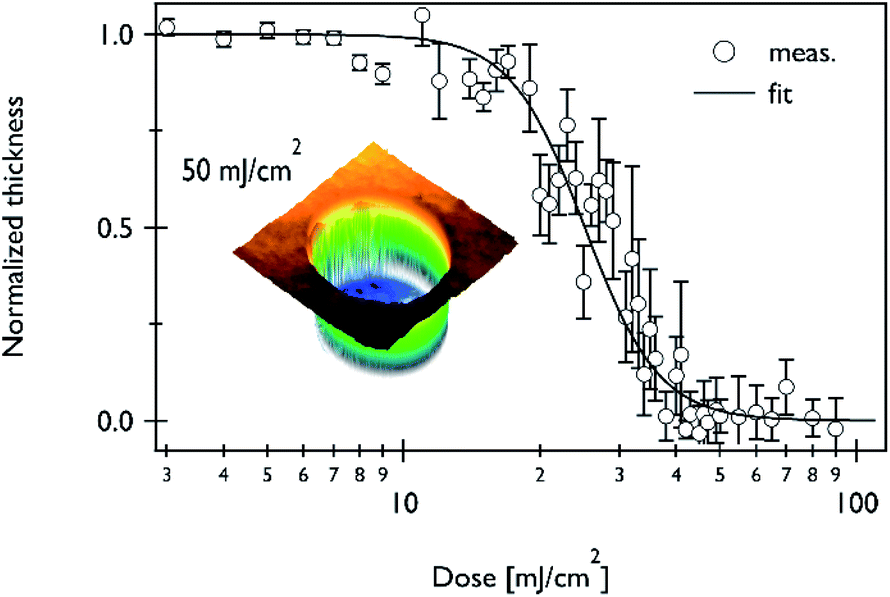 | ||
| Fig. 3 Experimentally measured contrast curve of PMMA (circle) and theoretically fitted response curve (line). Sensitivity E0 and contrast γ are 25.1 ± 0.5 mJ cm−2 and 5.3 ± 0.4, respectively. The insert presents the three-dimensional optical profile at 50 mJ cm−2. | ||
To determine the material properties, the results were fitted with a dose–response function:16,17
| D(E) = D0[1 + 10log(E0/E)×γ]−1. |
To investigate the dependence of the parameters, we performed the DCT with respect to the PMMA thickness. As shown in Fig. 4(a and b), the sensitivity linearly decreases as the sample thickness reduces. This feature is quite normal considering the Beer–Lambert law, in which light is exponentially deposited into the sample, ∼exp(−αt). The sensitivity of the thinnest sample, 75 nm, was 8.6 ± 0.5 mJ cm−2, which is consistent with values reported by Fallica et al. However, due to lack of data, it is barely determined that the sensitivity is saturated at <75 nm thickness. As shown in Fig. 4(c), the contrast shows similar values, ∼5, at a thickness of ≤160 nm. However, the contrast significantly increases thereafter. The measured optical penetration depth (1/α) of the PMMA layer at a 13.5 nm wavelength is approximately 190 nm, introduced in the later section and in the Henke table.28 Furthermore, considering the short mean free path of the secondary electrons in PMMA (on the order of a few nanometres),29,30 the ballistic transport is considerably suppressed owing to diffusive collision. Probably, after the optical depth, more kinetic energy of electrons is consumed to induce chemical reactions in PMMA. The correlation between the collisional process and contrast can be observed in the lithographic performance based on e-beam source. Here, the kinetic energy of electron is much higher than EUV source. Therefore, the energy gradient in photoresist is negligible. Experimentally, Yasin et al. reported a contrast of 5.4 for a 1 μm thick PMMA film.31 However, to understand this correlation, additional experiments and simulations must be necessary. Typically, to avoid the collapse of patterned line, recent researches have focused to achieve lithographic performance in thinner photoresist (normally, <30 nm).13,15,17,32 In that case, albeit photon energy is high enough (91.8 eV), most of electrons inducing structural changes of photoresist have low kinetic energy because it is generated via inelastic scattering from substrate.11,12 Therefore, studies to find proper thickness should be important. To quantitatively interpret these phenomena, additional experiments must be necessary to obtain the distribution of kinetic energy and/or collisional cross-section of energetic electrons by photoemission measurements.33 In addition, the dose–response function may be required to remodel the energy deposition dependence. In order to understand the lithographic performances at next generation source, such as beyond EUV, the function need to reflect the spatial distribution based on attenuation length.34
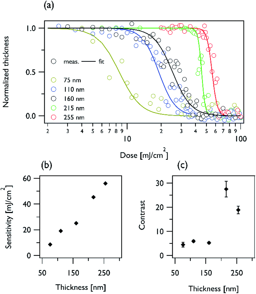 | ||
| Fig. 4 (a) DCT curves, (b) sensitivity, and (c) contrast as function of PMMA thickness. | ||
3.2. Transmission measurement
Fig. 5 shows the experimentally measured transmittance of PMMA at a 13.5 nm wavelength. PMMA films were coated on 200 nm thick Si3N4 substrates. The diameter of the incident beam was reduced to 220 μm through the pinhole aperture. In addition, as a probe beam, an intensity of 3 mW cm−2 was used to avoid a chemical reaction in the PMMA, as shown above the DCT.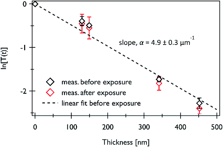 | ||
| Fig. 5 Experimentally measured transmittance in the PMMA film before (E = 0 mJ cm−2, black markers) and after (E = 200 mJ cm−2, red markers) exposure. The slope of the linear fit corresponds to the linear absorption coefficient in bare sample. | ||
Transmission was measured in the PMMA film before and after exposure. Under the exposure condition, the sample was fully equilibrated after irradiation with an EUV beam of 200 mJ cm−2. The mean and error values were obtained based on an average of approximately 100 and 10 shots, respectively, before and after the exposure. First, to determine the optical properties of the substrate, the transmittance of a bare Si3N4 membrane was measured using the same process. The resulting measured transmittance and error were used to determine the properties of the PMMA. According to the Beer–Lambert law, the transmittance can be described as a function of sample thickness D and linear absorption coefficient α: T(D) = exp(−αD). Thus, α can be determined on the basis of the slope of the linear fit of ln[T(D)]. In the bare PMMA film, the measured α of PMMA is 4.9 ± 0.3 μm−1. This result agrees well with the Henke table (approximately 5.2 μm−1) and previously published results.13,35,36 Thus, the measured value was applied in the calculation by the LPM. For the result after exposure, it is difficult to observe any change within the error scale. This observation also agrees with the findings of a previous work.13 Thus, we can ignore the optical parameters of chemically reacted molecules for the LPM.
3.3. Patterning performance
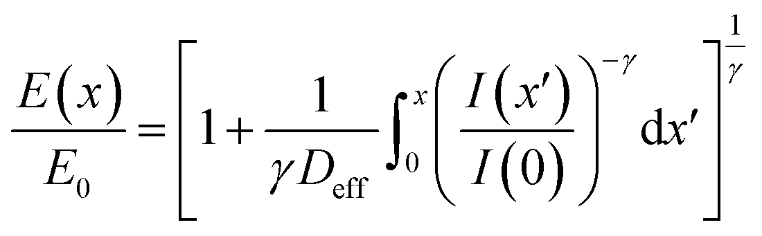
Fig. 6(a) shows the experimentally measured CD/pitch ratio as a function of the normalized dose E/E0, for a 160 nm thick PMMA film. The pitch size was 250 nm. Mean E0 (25.1 mJ cm−2) was calculated from the presented DCT results. We neglected the 2% error (the standard deviation of the mean) because it did not significantly affect the representative feature. In addition, we plotted the data from unity in the normalized dose because E0 represents the threshold energy. The numerical CD values were determined using the SuMMIT analysis software, which provides the CD and LER numbers on the basis of the SEM images. The mean and standard deviations were determined from 5–12 patterned lines in each SEM image. Overall, the CD/pitch ratio exponentially decreased with dose. At E/E0 > 2.5, the experimental data seemed to stabilize. We compared the observations with the curves calculated using the LPM:where E and I are the nominal exposure dose and aerial image intensity, respectively, Deff is the effective thickness based on
 . The sensitivity, E0, and contrast, γ, originate from the DCT results. Within the range of uncertainty, the observations agree well with the calculated curve at E/E0 < 2.5. Hereafter, although the discrepancy ratio is 15%, the data still agree well with the calculations. In addition, the results were compared with those of Fallica et al. obtained for 60 and 80 nm pitches.14 To obtain the patterns, they performed two-slit IL at 13.5 nm wavelength. Both datasets in their work showed similar dose-dependent CD/pitch ratios. Thus, the thickness of the resist affects the resolution of the lithographic patterns. Fig. 6(b) displays the corresponding LER as a function of the normalized dose. It linearly decreased below a normalised dose of approximately 2.5. Hereafter, the LER converges to approximately 11 nm, regardless of the exposure energy. At E/E0 < ∼2.5, the LER/CD ratio is improved (from ∼35% to ∼20%), shown in Fig. 6(c).
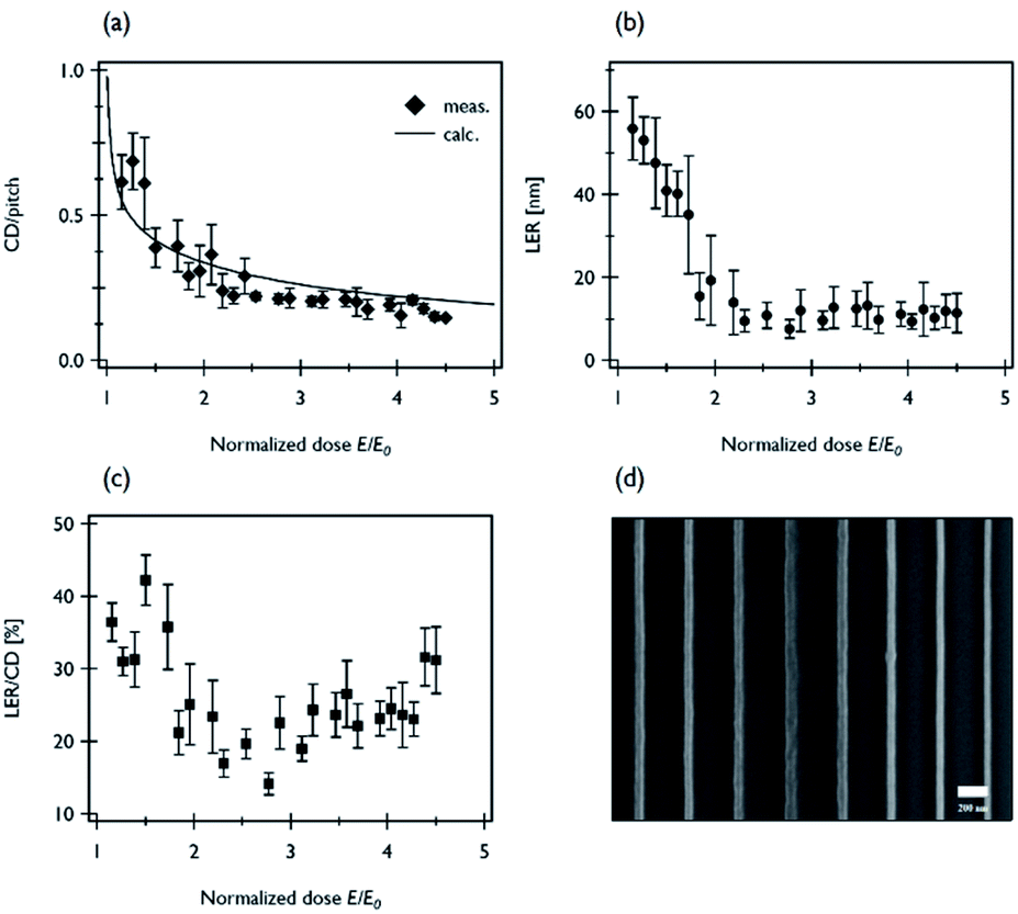 | ||
| Fig. 6 (a) Experimentally measured and calculated CD/pitch ratios as a function of normalized dose, (b) LER, and (c) LER/CD ratio. Error bars indicate one standard deviation of measurement. (d) SEM image taken at E/E0 = 3.5. | ||
4. Conclusions
Experimental and theoretical studies were performed to understand the lithographic performance characteristics of PMMA films based on DCTs, transmission measurements, and patterning tests. The sensitivity and contrast were slightly higher than those observed in a previously published study. This result may be related to the different thicknesses of the samples and/or the spectral properties of the EUV beam. In contrast, the linear absorption coefficient agreed well with the simulated values and the results from previously published works. In addition, the resolution of the lithographic patterns agreed well with the results calculated using the LPM on the basis of the measured parameters. The lithographic performance results of the PMMA demonstrate that our experimental apparatus is suitable for studying the optical properties of photoresists. This comprehensive study can play an important role in the discovery of novel photoresist candidates for applications in EUV lithography and even beyond EUV lithography.Author contributions
Kanghyun Kim: conceptualization, experiment, data analysis, writing. Jong-Won Lee: conceptualization, experiment, data analysis, data curation, writing. Byeong-Gyu Park: formal analysis, resources, review. Hyun-Taek Oh: conceptualization, formal analysis. Yejin Ku: conceptualization, formal analysis. Jin-Kyun Lee: conceptualization, review, funding acquisition. Geunbae Lim: supervision, review & editing. Sangsul Lee: conceptualization, funding acquisition, methodology, project administration, supervision, writing, review & editing.Conflicts of interest
There are no conflicts to declare.Acknowledgements
This research was supported by Samsung Research Funding & Incubation Center of Samsung Electronics (Project Number SRFC-TA1703-05, SRFC-TA1703-051) and the National Research Foundation of Korea (NRF) grant funded by the Korea government (MSIT) (NRF-2020M3H4A3081917). Experiments at PLS-II were supported in part by MSIT and POSTECH.Notes and references
- H. Kinoshita, K. Kurihara, Y. Ishii and Y. Torii, J. Vac. Sci. Technol., B: Microelectron. Process. Phenom., 1989, 7, 1648–1651 CrossRef CAS.
- J. Bjorkholm, J. Bokor, L. Eichner, R. Freeman, J. Gregus, T. Jewell, W. Mansfield, A. Mac Dowell, E. Raab and W. Silfvast, J. Vac. Sci. Technol., B: Microelectron. Process. Phenom., 1990, 8, 1509–1513 CrossRef CAS.
- P. Thibault, M. Dierolf, A. Menzel, O. Bunk, C. David and F. Pfeiffer, Science, 2008, 321, 379–382 CrossRef CAS PubMed.
- Y. Ekinci, H. H. Solak, C. Padeste, J. Gobrecht, M. P. Stoykovich and P. F. Nealey, Microelectron. Eng., 2007, 84, 700–704 CrossRef CAS.
- J. van Schoot, E. van Setten, G. Rispens, K. Z. Troost, B. Kneer, S. Migura, J. T. Neumann and W. Kaiser, J. Micro/Nanolithogr., MEMS, MOEMS, 2017, 16, 041010 Search PubMed.
- N. Mojarad, J. Gobrecht and Y. Ekinci, Microelectron. Eng., 2015, 143, 55–63 CrossRef CAS.
- M. Goldstein, R. Hudyma, P. Naulleau and S. Wurm, Opt. Lett., 2008, 33, 2995–2997 CrossRef PubMed.
- M. Niibe, Y. Kakutani, K. Kakiuchi, S. Terashima, H. Takase, Y. Gomei, T. Aoki, S. Matsunari, H. Kondo and Y. Fukuda, Jpn. J. Appl. Phys., 2005, 44, 5552 CrossRef CAS.
- S. Sun and G. J. Leggett, Nano Lett., 2004, 4, 1381–1384 CrossRef CAS.
- T. Ito and S. Okazaki, Nature, 2000, 406, 1027–1031 CrossRef CAS PubMed.
- B. Cord, J. Yang, H. Duan, D. C. Joy, J. Klingfus and K. K. Berggren, J. Vac. Sci. Technol., B: Microelectron. Nanometer Struct.–Process., Meas., Phenom., 2009, 27, 2616–2621 CrossRef CAS.
- J. Torok, R. Del Re, H. Herbol, S. Das, I. Bocharova, A. Paolucci, L. E. Ocola, C. Ventrice Jr, E. Lifshin and G. Denbeaux, J. Photopolym. Sci. Technol., 2013, 26, 625–634 CrossRef CAS.
- R. Fallica, J. K. Stowers, A. Grenville, A. Frommhold, A. P. Robinson and Y. Ekinci, J. Micro/Nanolithogr., MEMS, MOEMS, 2016, 15, 033506 CrossRef.
- R. Fallica, R. Kirchner, Y. Ekinci and D. Mailly, J. Vac. Sci. Technol., B: Nanotechnol. Microelectron.: Mater., Process., Meas., Phenom., 2016, 34, 06K702 Search PubMed.
- R. Fallica, D. Kazazis, R. Kirchner, A. Voigt, I. Mochi, H. Schift and Y. Ekinci, J. Vac. Sci. Technol., B: Nanotechnol. Microelectron.: Mater., Process., Meas., Phenom., 2017, 35, 061603 Search PubMed.
- Y. Ekinci, M. Vockenhuber, M. Hojeij, L. Wang and N. Mojarad, Extreme Ultraviolet (EUV) Lithography IV, 2013, vol. 8679, p. 867910 Search PubMed.
- E. Buitrago, O. Yildirim, C. Verspaget, N. Tsugama, R. Hoefnagels, G. Rispens and Y. Ekinci, Extreme Ultraviolet (EUV) Lithography VI, 2015, vol. 9422, p. 94221S Search PubMed.
- B. Griffing and P. West, Polym. Eng. Sci., 1983, 23, 947–952 CrossRef CAS.
- H.-T. Oh, S.-H. Jung, K.-H. Kim, Y. Moon, D. H. Jeong, Y. Ku, S. Lee, B.-G. Park, J. Lee and C. Koh, RSC Adv., 2021, 11, 1517–1523 RSC.
- P. G. Reddy, N. Mamidi, P. Kumar, S. K. Sharma, S. Ghosh, K. E. Gonsalves and C. P. Pradeep, RSC Adv., 2016, 6, 67143–67149 RSC.
- R. T. Frederick, S. Saha, J. T. Diulus, F. Luo, J. M. Amador, M. Li, D.-H. Park, E. L. Garfunkel, D. A. Keszler and G. S. Herman, Microelectron. Eng., 2019, 205, 26–31 CrossRef CAS.
- E. Vogel, Nat. Nanotechnol., 2007, 2, 25–32 CrossRef CAS PubMed.
- N. G. Orji, M. Badaroglu, B. M. Barnes, C. Beitia, B. D. Bunday, U. Celano, R. J. Kline, M. Neisser, Y. Obeng and A. Vladar, Nat. Electron., 2018, 1, 532–547 CrossRef PubMed.
- L. Wang, D. Fan, V. A. Guzenko and Y. Ekinci, J. Vac. Sci. Technol., B: Nanotechnol. Microelectron.: Mater., Process., Meas., Phenom., 2013, 31, 06F602 Search PubMed.
- H. H. Solak, C. Dais and F. Clube, Opt. Express, 2011, 19, 10686–10691 CrossRef CAS PubMed.
- V. Bakshi, EUV sources for lithography, 2006, vol. 1, pp. 3–25 Search PubMed.
- A. Rathore, I. Pollentier, H. Singh, R. Fallica, D. De Simone and S. De Gendt, J. Mater. Chem. C, 2020, 8, 5958–5966 RSC.
- A. Thompson, I. Lindau, D. Attwood, Y. Liu, E. Gullikson, P. Pianetta, M. Howells, A. Robinson, K.-J. Kim, J. Scofield, J. Kirz, J. Underwood, J. Kortright, G. Williams and H. Winick, X-ray data booklet, Lawrence Berkeley National Laboratory, University of California, Berkeley, 2009 Search PubMed.
- R. Roberts, D. Allara, C. Pryde, D. Buchanan and N. Hobbins, Surf. Interface Anal., 1980, 2, 5–10 CrossRef CAS.
- P. de Vera, I. Abril and R. Garcia-Molina, J. Appl. Phys., 2011, 109, 094901 CrossRef.
- S. Yasin, D. Hasko and H. Ahmed, Microelectron. Eng., 2002, 61, 745–753 CrossRef.
- X. Wang, L.-T. Tseng, D. Kazazis, Z. Tasdemir, M. Vockenhuber, I. Mochi and Y. Ekinci, J. Micro/Nanolithogr., MEMS, MOEMS, 2019, 18, 013501 CAS.
- J. Ma, P. Naulleau, M. Ahmed and O. Kostko, J. Appl. Phys., 2020, 127, 245301 CrossRef.
- N. Mojarad, J. Gobrecht and Y. Ekinci, Sci. Rep., 2015, 5, 1–7 Search PubMed.
- G. D. Kubiak, E. M. Kneedler, R. Q. Hwang, M. T. Schulberg, K. W. Berger, J. Bjorkholm and W. Mansfield, J. Vac. Sci. Technol., B: Microelectron. Nanometer Struct.–Process., Meas., Phenom., 1992, 10, 2593–2599 CrossRef CAS.
- N. N. Matsuzawa, H. Oizumi, S. Mori, S. Irie, E. Yano, S. Okazaki and A. Ishitani, Microelectron. Eng., 2000, 53, 671–674 CrossRef CAS.
Footnote |
| † These authors contributed equally. |
| This journal is © The Royal Society of Chemistry 2022 |