
 Open Access Article
 This Open Access Article is licensed under a
 Creative Commons Attribution 3.0 Unported Licence
Chemical vapor deposition merges MoS2 grains into high-quality and centimeter-scale films on Si/SiO2†
Mukesh Singha,
Rapti Ghoshbcd,
Yu-Siang Chenc,
Zhi-Long Yena,
Mario Hofmann a,
Yang-Fang Chena and
Ya-Ping Hsieh*cd
a,
Yang-Fang Chena and
Ya-Ping Hsieh*cd
aDepartment of Physics, National Taiwan University, Taipei 106, Taiwan
bDepartment of Physics, National Central University, Chung Li 320, Taiwan
cInstitute of Atomic and Molecular Sciences, Academia Sinica, Taipei 115, Taiwan. E-mail: yphsieh@gate.sinica.edu.tw
dMolecular Science and Technology, Taiwan International Graduate Program, Academia Sinica, Taipei 115, Taiwan
First published on 18th February 2022
Abstract
Two-dimensional molybdenum disulfide (MoS2) has attracted increasing attention due to its promise for next-generation electronics. To realize MoS2-based electronics, however, a synthesis method is required that produces a uniform single-layer material and that is compatible with existing semiconductor fabrication techniques. Here, we demonstrate that uniform films of single-layer MoS2 can be directly produced on Si/SiO2 at wafer-scale without the use of catalysts or promoters. Control of the precursor transport through oxygen dosing yielded complete coverage and increased connectivity between crystalline MoS2 domains. Spectroscopic characterization and carrier transport measurements furthermore revealed a reduced density of defects compared to conventional chemical vapor deposition growth that increased the quantum yield over ten-fold. To demonstrate the impact of enhanced scale and optoelectronic performance, centimeter-scale arrays of MoS2 photosensors were produced that demonstrate unprecedentedly high and uniform responsivity. Our approach improves the prospect of MoS2 for future applications.
Introduction
Molybdenum disulfide (MoS2) is a 2D material that has attracted the attention of researchers due to its unique electrical and optical properties.1 Based on its high carrier mobility,2,3 electrostatic controllability,4 environment stability,5 and thickness-induced bandgap tunability,6,7 MoS2 is considered an enabling material for future electronics.8,9 This promise is corroborated by the reported impressive performance of MoS2 in optoelectronic devices such as photodetectors,10–15 light emitters,16,17 and haptic sensors.18However, to advance MoS2-based electronics from research into commercially viable applications, MoS2 production has to be compatible with existing, mature semiconductor fabrication technology. This requirement disqualifies mechanical exfoliation due to small crystallite size and unreliable placement. Moreover, synthesis on single-crystalline substrates such as sapphire,19 h-BN, mica20–23 and metal24,25 cannot be employed, despite their impressive performance, as the required large-scale and high-precision transfer step are beyond current capabilities. The most promising approach is the direct growth of MoS2 on silicon dioxide (SiO2) due to the experience of semiconductor industry with the material system8,26 and the existing commercial infrastructure. Unfortunately the growth on SiO2, to date, has only yielded discontinuous flakes compared to the uniform and continuous films grown on other substrates.27–29 Several approaches have been explored to overcome this challenge but they introduce other issues. First, the use of organic seeding materials like perylene-3,4,9,10-tetracarboxylic acid tetrapotassium salt (PTAS) can enhance the continuity of MoS2 but introduces impurities into the reactor and into the produced MoS2.30,31 Second, large grain sizes and continuous films can be achieved by liquid-substrate chemical vapour deposition (CVD) but salt-residue remains on the SiO2.32
In this study, we have introduced an approach to produce continuous single layer MoS2 at large-scale on Si/SiO2. This advance was accomplished by a modified CVD process that utilizes a small amount of oxygen. Using this method, high quality material with unprecedented continuity and uniformity could be synthesized, as evidenced by spectroscopic characterization and electron microscopy. The resulting material was applied to MoS2-based optoelectronic devices that demonstrate record-breaking performance and uniform properties throughout wafer-scale device array.
Results and discussion
Chemical vapor deposition is an established process to synthesize MoS2 from gaseous precursors.33–35 We employ silicon oxide wafers as substrates and observe discontinuous triangular flakes with average dimensions of ∼10 μm size (Fig. 1(a)) when using established CVD parameters.33,36 Even long growth durations cannot connect these individual flakes, raising the question as to the limiting mechanism. The MoS2 growth by CVD is a multistep conversion process from gaseous MoO3 precursor into adsorbed species that are subsequently integrated into the outgrowing MoS2 crystal.37 The self-limiting grain size indicates the kinetic hindrance of precursor supply at long growth durations: at low MoS2 coverage, adsorption of MoO3 precursor proceeds quickly and flake growth occurs. At high MoS2 coverage, however, the adsorption efficiency decreases as less uncovered surface sites are available. Consequently, the MoS2 growth rate decreases until precursor adsorption and desorption are in equilibrium, and no further growth occurs (Fig. 1(b)).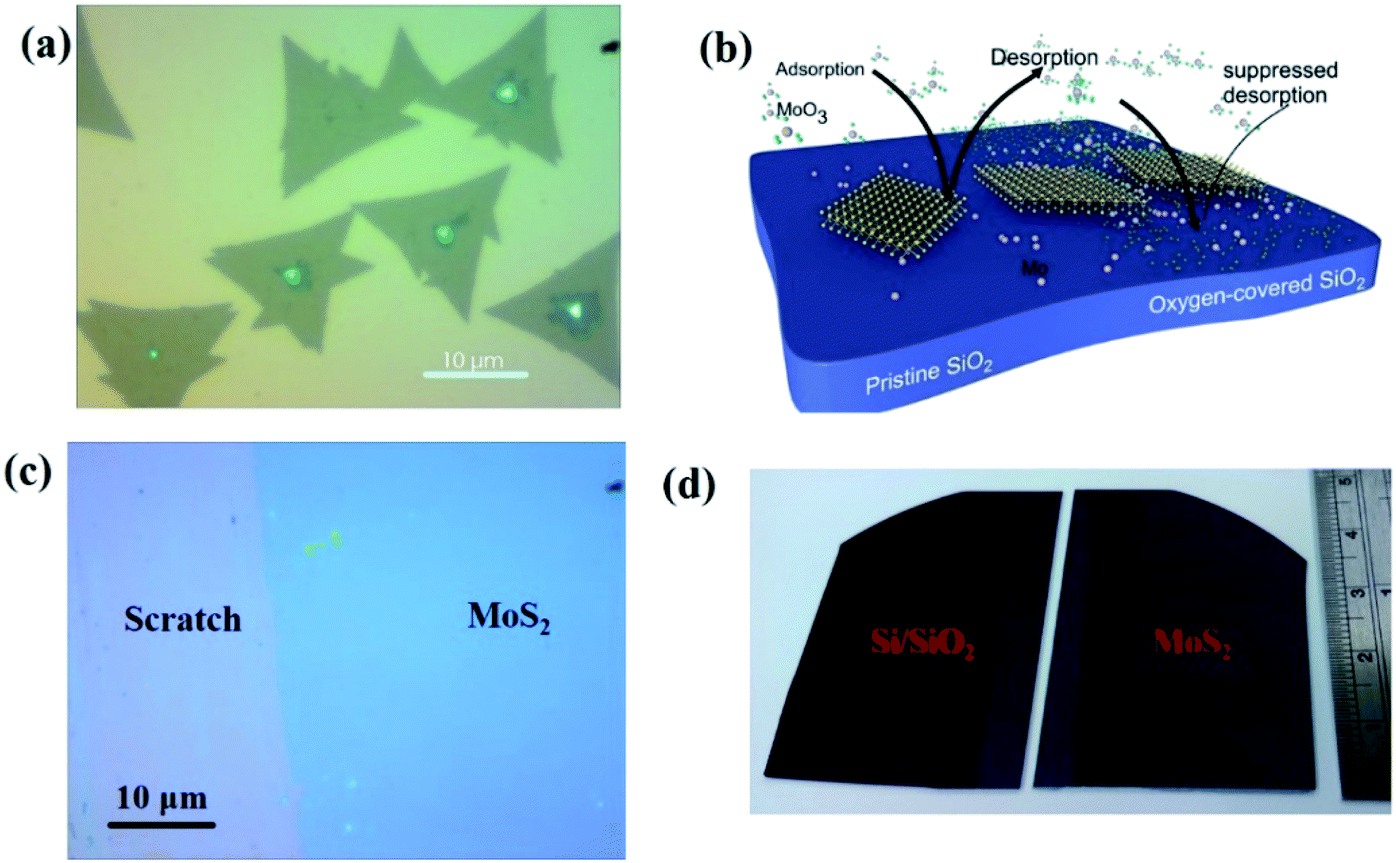 | ||
| Fig. 1 (a) Optical microscopy image of MoS2 films as deposited on Si/SiO2 substrate without O2. (b) Schematic of adsorption and desorption of gaseous phase MoO3 on Si/SiO2. (c) Optical microscopy image (taken after scratch the film gently by tweezer) of in situ O2 processed samples. (d) Camera image of wafer scale continuous MoS2 on Si/SiO2 (in right) and a blank Si/SiO2 substrate (in left) for the reference. | ||
We overcome this limitation by introducing 0.5 sccm of oxygen. Previous work has demonstrated that increased chemisorption of oxygen on silicon oxide surfaces stabilizes the MoO3 precursor38 and thus reduces the impact of precursor desorption on growth rate (Fig. 1(b)). Indeed, optical microscopy images demonstrate that the addition of oxygen during the CVD growth process produces continuous films (Fig. 1(c)). The modified oxygen-assisted CVD method can also grow uniform and continuous wafer-scale MoS2 (Fig. 1(d)). Detailed characterization of the oxygen-grown MoS2 by atomic force microscopy (AFM) corroborates the high uniformity of the film (Fig. 2a). The thickness of ∼1 nm presents a clear evidence of uniform single-layer MoS2 films39,40 (more details about the uniformity of the films can be found in the ESI S1†). This evaluation is confirmed by Raman spectra which show characteristic peaks at 382 ± 0.5 cm−1 and 404 ± 0.5 cm−1 corresponding to in-plane E12g mode and out-of-plane A1g mode, respectively (Fig. 2b). These two peaks are well separated by 22 ± 0.5 cm−1, which indicates the single/bi layer nature MoS2 film.39,41,42 Raman mapping was employed to characterize the uniformity of the MoS2. Fig. 2c(i and ii) shows the spatial distribution of the E12g and A1g peaks postion over a 100 × 100 μm2 area with a step size of 1 μm, demonstrating the absence of vacancies and the uniform peak separation of ∼22 ± 0.5 cm−1 throughout the film. TEM images (Fig. 3a(i) and b(i)) further corroborate the uniformity for both type of the films. The selected area electron diffraction (SAED) (Fig. 3a(ii) and b(ii)) and high-resolution transmission electron microscopy (HRTEM) (Fig. 3a(iii) and b(iii)) indicate the polycrystalline nature of O2-assisted MoS2 in comparison to conventional MoS2, where single crystal characteristic was observed. Apart from the optical characterizations, films were further characterized by electrical transport measurement in co-planar geometry for the centimetre scale area of MoS2 continuity. Fig. 3c and d represent the electrical sheet conductance and electrical current respectively, in two terminal co-planar geometry, for the device with different channel length of 50, 100, 150, 200 and 250 μm and at a fixed channel width of 580 μm. Each channel length belonging to one particular row and there are five row in the device. So, the data shown here is for 25 devices. The uniformity of current in MoS2 shows that films are continuous in centimetre scale. The current variation in each row indicates the polycrystalline nature of MoS2 films.
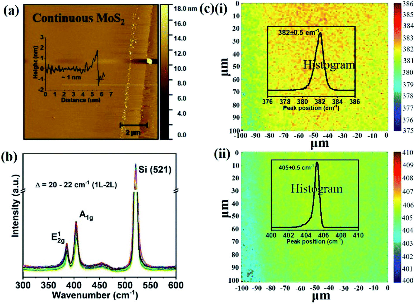 | ||
| Fig. 2 Characterization of in situ O2 processed continuous MoS2 films on Si/SiO2 (a) AFM image (scale bar: 2 μm) (height profile given in inset). (b) Raman spectra of the as deposited films measured at several randomly selected locations. (c) Raman mapping of (i) E12g and (ii) A1g peak positions in 100 μm × 100 μm dimensions with 1 μm step size (histogram shown in inset). | ||
 | ||
| Fig. 3 (a and b) TEM characterization of conventional (a) and oxygen-assisted (b) MoS2:(i) low resolution TEM image after transfer onto carbon-coated grid, (ii) SAED pattern (scale bar: 5 nm−1) (iii) HRTEM image (scale bar: 2 nm). Electrical characterization of uniformity: histogram of sheet conductance for 18 devices (c) in device array (see inset, (c)). Demonstration of channel continuity through current measurements within large device array of different channel lengths measured at fixed bias of 20 V in two terminal co-planar geometry. | ||
The effect of adding oxygen was further investigated by photoelectron spectroscopy. X-ray photoelectron spectroscopy (XPS) demonstrate peaks corresponding to S 2s, Mo4+ 3d5/2 and Mo4+ 3d3/2 (indicating MoS2) at 226.7 eV, 229.6 eV, 232.8 eV, respectively (Fig. 4(a) and (b)). Along with the Mo4+ oxidation states, a small fraction of higher oxidation states was also observed, such as peaks at 233.6 eV and 235.9 eV corresponding to Mo6+ 3d5/2 and Mo6+ 3d3/2 respectively, for the in situ oxygen processed samples (Fig. 4(b)).43,44 These higher oxidation states could indicate molybdenum oxide formation, but their concentration is less than 7% (estimated from the fitted area of MoS2 and MoO3 oxidation), which could indicate their origin as surface contaminants.
 | ||
| Fig. 4 XPS spectra of Mo 3d binding energy for the films deposited (a) without O2 and (b) with in situ O2 samples. (c) PL spectra of single layer MoS2 for both the films; without O2 and with in situ O2. (d and e) Deconvoluted PL spectra of MoS2 without O2 and with in situ O2 processed samples respectively. (f) Schematic energy level diagram of conventional MoS2 (i.e. without O2) and oxygen-assisted MoS2 films. | ||
The high crystallinity of oxygen-assisted MoS2 growth can be inferred from photoluminescence (PL) spectroscopy. Comparable to conventional MoS2, oxygen-assisted MoS2 shows a prominent peak near 1.8 eV which corresponds to the direct bandgap absorption of single-layer MoS2 (Fig. 4(c)).45 Surprisingly, an enhancement of PL peak intensity for oxygen-assisted CVD over conventional MoS2 by 15 times can be seen. This significant increase in quantum yield provides an exciting route towards improving MoS2 optoelectronic performance without the need for post-growth treatment.46 Detailed characterization of the PL spectra (Fig. 4(d) and (e)) demonstrates a decrease in the concentration of charged excitons (i.e. trions) and a subsequent increase of the neutral exciton emission for O2 processed samples. The schematic energy level diagram of conventional and oxygen-assisted MoS2 is shown in Fig. 4(f), where transitions of excitons and trions are shown.
To identify the reason for this difference, we conduct Kelvin probe measurements. The work function for individual triangle MoS2 samples (O2 free) was 4.34 eV, whereas the work-function of in situ oxygen processed samples was increased to 4.73 eV. The increase of work function in in situ O2 processed samples indicates that the usually n-type material is rendered more neutral.47 This effect could be due to the decrease in sulfur vacancies that cause n-type doping.48
These results indicate that the enhanced quantum yield's origin is a decrease in nonradiative recombination through trion states brought about by a lowered defect-induced doping.49
We illustrate the potential of the increased scale and quality of MoS2 growth by producing electronic device arrays. As a first example, transistor devices were fabricated using photo-lithography (Fig. 5(a)) (more details on the device fabrication can be found in the ESI S2†). The transfer curves of oxygen-processed MoS2 show a higher threshold voltage than conventionally grown MoS2, which corroborates the observed decrease in n-type character (Fig. 5(b)). Notably, the transistor channel for O2 grown MoS2 includes many polycrystalline regions, whereas the conventional grown MoS2 transistor was designed around a single-crystalline flake (Fig. 5(a)), necessitating complex alignment schemes. Consequently, the observed transfer characteristics of the O2-grown MoS2 represent an averaging of the conductivity from the dozens of individual flakes and their boundaries. Despite this disadvantage, the transfer characteristics of large scale O2 grown MoS2 exhibits a similar behaviour as microscopic MoS2 crystals, indicating the good connectivity between polycrystalline regions. The measured field-effect mobility for both device types is within the range 0.1–10 cm2 V−1 s−1 of previous results in the literature for the similar structure of back gated MoS2 field-effect transistor devices.50,51
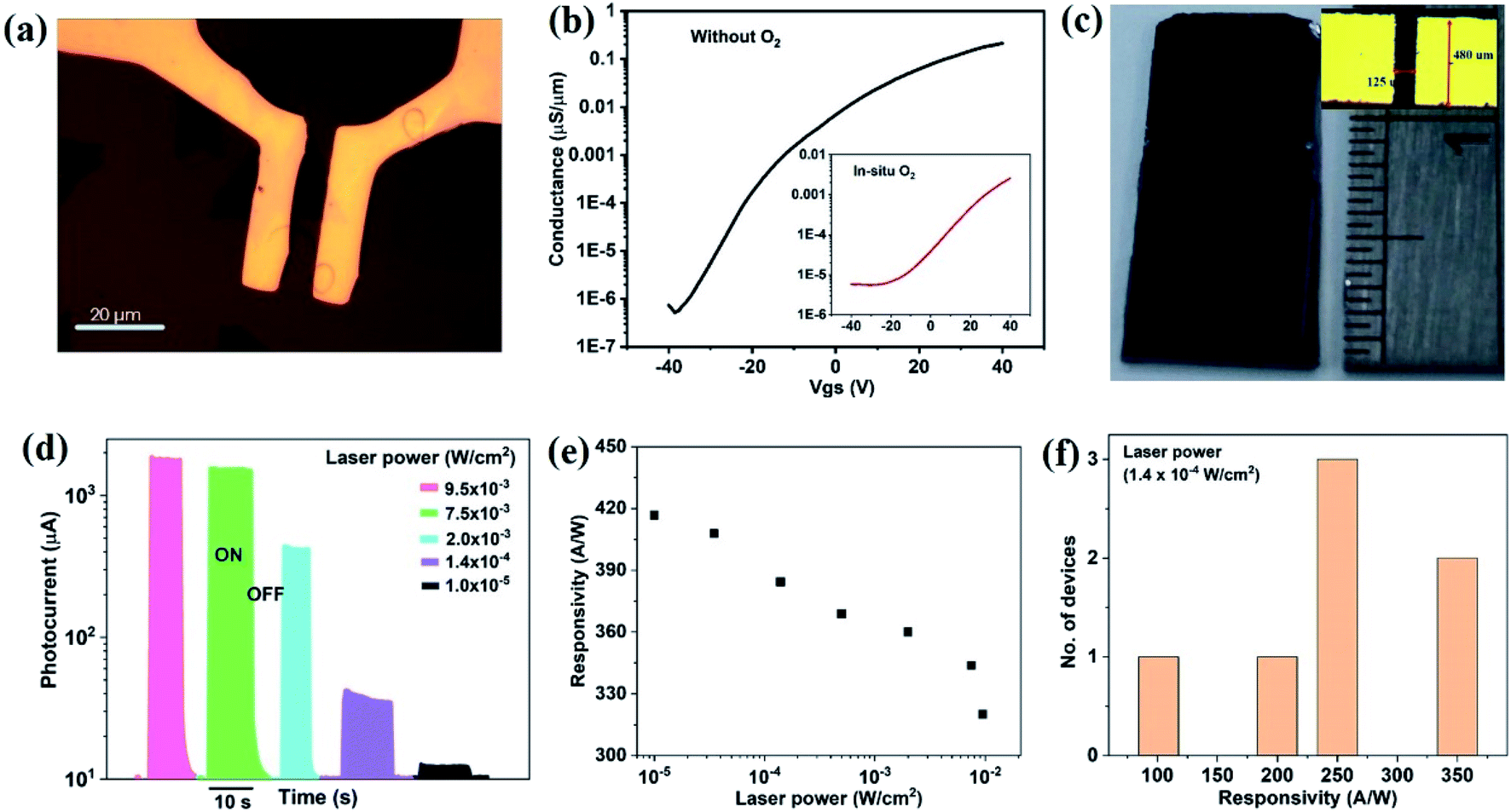 | ||
| Fig. 5 (a) Optical microscopy image of MoS2 back gate field effect transistor with channel length 6 μm (scale bar 20 μm). (b) Transfer characteristic of individual triangular MoS2 domains with fixed bias voltage (Vds) 10 V (for continuous MoS2 films, transfer characteristic shown in inset). Photosensor characteristics of in situ O2 processed continuous MoS2 films; (c) camera image of large area MoS2 photosensor array in centimetre dimension (channel length = 125 μm), (d) photocurrent variation with different laser power, (e) responsivity of the device with different laser power, (f) average responsivity of the MoS2 films shown at fixed power of 1.4 × 10⁻⁴ W cm−2. | ||
As a second application of MoS2 high optoelectronic performance, we produce centimeter-scale photosensor arrays (Fig. 5(c)). A variable photocurrent (Iph) was observed when toggling illumination with different laser power (Fig. 5(d)). The responsivity (R) of the device, defined as the ratio of photocurrent to the incident power (Pin), increases with decreasing laser power (Fig. 5(e)) and reaches values in excess of ∼420 A W−1 in two-terminal co-planar geometry. This value represents the quite higher responsivity of MoS2 as compared to other reports11,41,52,53 (for a comparison to literature, see the ESI S3†) and indicates the benefits of producing MoS2 with low trap density and efficient carrier conduction. More importantly, uniformly high responsivity could be achieved for all devices throughout the centimetre-sized samples (Fig. 5(f)). The stability of photosensor also performed using I–T measurement for 10 cycles and details are given in the ESI S4.† In the support of large scale photodetector array, a uniform photosensitivity of MoS2 on Si/SiO2 is shown in ESI S5,† where, wafer scale photosensitivity is demonstrated (Table 1).
| Responsivity (A W−1) | Wavelength and laser power | Area of devices (L/W) (in μm) | Materials | References |
|---|---|---|---|---|
| 1 at Vds = 1.5 V | 532 nm, 200 μW | A few micron/tens to 100 micron | CVD MoS2 | 1 |
| 1 × 10⁻³ at Vds = 1 V | 405 nm, 100 μW | 2/20 | CVD MoS2 | 2 |
| 59 at Vds = 1.2 V | 532 nm, 1.69 × 10⁻³ W cm−2 | 5/∼30 | Exfoliated MoS2 | 3 |
| 780 at Vds = 1 V | 532 nm, 1.3 × 10⁻⁴ W cm−2 | — | CVD MoS2 | 4 |
| 1.1 × 10⁶ at Vds = 0.15 V | 460 nm, 0.33 pW | — | Exfoliated MoS2 | 5 |
| 1.1 × 10⁻³ at Vds = 1.5 V | 514.5 nm, 1 μW | 0.8/5 | CVD MoS2 | 6 |
| 0.42 × 10⁻³ at Vds = 1 V | 550 nm, 80 W cm−2 | 2.1/2.6 | Exfoliated MoS2 | 7 |
| 7 at Vds = 1 V | 488 nm, 1 μW | — | CVD MoS2 | 8 |
| 420 at Vds = 15 V | 532 nm, 10−5 W cm−2 | 125/480 | CVD MoS2 | This work |
Conclusion
Continuous single-layer MoS2 films on Si/SiO2 substrates were successfully fabricated through an oxygen-assisted CVD growth process. Modification of the precursor transport resulted in highly crystalline material with well-interconnected domains. The absence of defects was shown to decrease the n-type doping of MoS2 and enhance its optoelectronic performance. Large array of highly sensitive photosensors were produced that exhibit uniform and 200-fold increased responsivities over the entire substrate as compared to other reports. The presented combination of increased MoS2 quality, scale, and commercial appeal open up new routes towards the future of 2D materials.Experimental section
MoS2 synthesis
MoS2 thin films on Si/SiO2 were prepared by a CVD process, where 3 inch quartz tube furnace, having three different heating zone, was used. Si/SiO2 substrates were cleaned by sonication in acetone for 15 min, and then isopropyl alcohol followed by water wash and then dry with N2 gun. MoO3 powder (20 mg) was placed into two alumina boat (10 mg in each) at the lower heating zone furnace, which was upstream relative to center zone furnace. H2S gas (99% diluted with Ar) 400 sccm was used as a source of sulfur. It also acts as a carrier gas for MoO3 vapor to react with H2S and get deposited on the substrate. Separate Ar gas of 100 sccm was also used in the process. Substrate was placed at the center zone furnace facing polished surface upside and kept at a distance of 20 cm downstream relative to MoO3 powder. MoS2 films were deposited for 40 min at a low process pressure of 4 torr. Substrates were placed at 900 °C in the centre zone furnace, while MoO3 powder were placed at lower temperature of 750 °C. After purging the furnace with pure Ar for 1 h, furnace was heated to 600 °C at a heating rate of 30 °C min−1 and then maintained at the same temperature for 5 min. Further, temperature was increased to 900 °C at a rate of 30 °C min−1. A small amount of oxygen (0.5 sccm) was also added during the deposition. After completion, furnace was cooled down naturally. Here, we have only reported for the films deposited with O2 0.5 sccm, because with higher oxygen rate the pressure inside the furnace was not stable and started to keep on increasing with increasing process time.MoS2 characterization
The surface morphology of the samples was characterized by AFM (model: Veeco, Dimension Icon) and TEM (model: JEOL, JEM-2100F) measurements. Raman spectra and PL measurements (model: HORIBA, Jobin Yvon Technology iHR 550) were recorded under ambient using a laser excitation wavelength of 532 nm. Laser spot size was ∼1 μm2 and laser power at the sample surface was 3 mW. Chemical configuration was characterized by XPS (model: ULVAC-PHI, PHI Quanterall), where XPS peak was calibrated with C 1s (284.6 eV). Work function of the sample surface was measured by Kelvin probe force microscopy (model: KP Technology Ltd., DCU series-10) using Pt coated tip in non-contact mode. The cantilever tip was calibrated using a standard Au plate electrode.Author contributions
M. S. synthesis of MoS2 films via CVD and also fabricated the devices and performed the electrical and optical measurements. M. S., Y. S.-C., and Z. L.-Y. analyzed Raman and AFM measurements. R. G. and M. S. performed the photosensor measurements and analyzed the responsivity data. Y. P.-H., Y. F.-C., and M. H. supervised the project. M. S., Y. P.-H., Y. F.-C., and M. H. have contributed to writing the paper through the input of all the authors.Conflicts of interest
There are no conflicts to declare.Acknowledgements
This work is financially supported by the Ministry of Science and Technology, Taiwan (Grant No. MOST107-2112-M-002-004-MY3, MOST107-2119-M-001-032-MY3 and MOST108-2112-M-001-040-MY3). Also, authors would like to acknowledge Centre for Emerging Material and Advanced Devices, National Taiwan University, Taiwan, for providing characterization facilities.References
- Y. L. Huang, Y. Chen, W. Zhang, S. Y. Quek, C. Chen, L. Li, W. Hsu, W. Chang, Y. J. Zheng, W. Chen and A. T. S. Wee, Nat. Commun., 2015, 6, 6298 CrossRef PubMed.
- J. Jeon, S. K. Jang, S. M. Jeon, G. Yoo, Y. H. Jang, J. H. Park and S. Lee, Nanoscale, 2015, 7, 1688–1695 RSC.
- B. Radisavljevic, A. Radenovic, J. Brivio, V. Giacometti and A. Kis, Nat. Nanotechnol., 2011, 6, 147–150 CrossRef CAS PubMed.
- A. Azcatl, X. Qin, A. Prakash, C. Zhang, L. Cheng, Q. Wang, N. Lu, M. J. Kim, J. Kim, K. Cho, R. Addou, C. L. Hinkle, J. Appenzeller and R. M. Wallace, Nano Lett., 2016, 16, 5437–5443 CrossRef CAS PubMed.
- P. Budania, P. Baine, J. Montgomery, C. McGeough, T. Cafolla, M. Modreanu, D. McNeill, N. Mitchell, G. Hughes and P. Hurley, MRS Commun., 2017, 7, 813–818 CrossRef CAS.
- K. F. Mak, C. Lee, J. Hone, J. Shan and T. F. Heinz, Phys. Rev. Lett., 2010, 105, 136805 CrossRef PubMed.
- J. K. Ellis, M. J. Lucero and G. E. Scuseria, Appl. Phys. Lett., 2011, 99, 261908 CrossRef.
- H. Wang, L. Yu, Y. H. Lee, Y. Shi, A. Hsu, M. L. Chin, L. J. Li, M. Dubey, J. Kong and T. Palacios, Nano Lett., 2012, 12, 4674–4680 CrossRef CAS PubMed.
- P. V. K. Yadav, B. Ajitha, Y. A. Kumar Reddy and A. Sreedhar, Chemosphere, 2021, 279, 130473 CrossRef CAS PubMed.
- Z. Yin, H. Li, H. Li, L. Jiang, Y. Shi, Y. Sun, G. Lu, Q. Zhang, X. Chen and H. Zhang, ACS Nano, 2012, 6, 74–80 CrossRef CAS PubMed.
- N. Perea-López, Z. Lin, N. R. Pradhan, A. Iñiguez-Rábago, A. L. Elías, A. McCreary, J. Lou, P. M. Ajayan, H. Terrones, L. Balicas and M. Terrones, 2D Mater., 2014, 1, 011004 CrossRef.
- P. V. K. Yadav, B. Ajitha, Y. A. Kumar Reddy and V. R. Minnam Reddy, ACS Appl. Electron. Mater., 2021, 3, 2056–2066 CrossRef CAS.
- P. V. K. Yadav, B. Ajitha, V. Annapureddy, Y. A. K. Reddy and A. Sreedhar, Mater. Lett., 2021, 301, 130296 CrossRef CAS.
- P. V. K. Yadav, B. Ajitha, Y. A. K. Reddy, V. R. M. Reddy, M. Reddeppa and M. D. Kim, Appl. Surf. Sci., 2021, 536, 147947 CrossRef.
- P. V. K. Yadav, Y. A. K. Reddy, B. Ajitha and V. R. M. Reddy, J. Alloys Compd., 2020, 816, 152565 CrossRef CAS.
- E. Singh, P. Singh, K. S. Kim, G. Y. Yeom and H. S. Nalwa, ACS Appl. Mater. Interfaces, 2019, 11, 11061–11105 CrossRef CAS PubMed.
- W. Zhang, P. Zhang, Z. Su and G. Wei, Nanoscale, 2015, 7, 18364–18378 RSC.
- M. Park, Y. J. Park, X. Chen, Y. K. Park, M. S. Kim and J. H. Ahn, Adv. Mater., 2016, 28, 2556–2562 CrossRef CAS PubMed.
- H. Yu, M. Liao, W. Zhao, G. Liu, X. J. Zhou, Z. Wei, X. Xu, K. Liu, Z. Hu, K. Deng, S. Zhou, J. A. Shi, L. Gu, C. Shen, T. Zhang, L. Du, L. Xie, J. Zhu, W. Chen, R. Yang, D. Shi and G. Zhang, ACS Nano, 2017, 11, 12001–12007 CrossRef CAS PubMed.
- D. Dumcenco, D. Ovchinnikov, K. Marinov, P. Lazic, M. Gibertini, N. Marzari, O. L. Sanchez, Y. Kung, D. Krasnozhon, M. Chen, S. Bertolazzi, P. Gillet, A. Fontcuberta, A. Radenovic and A. Kis, ACS Nano, 2015, 9, 4611–4620 CrossRef CAS PubMed.
- F. Zhang, Y. Wang, C. Erb, K. Wang, P. Moradifar, V. H. Crespi and N. Alem, Phys. Rev. B, 2019, 99, 155430 CrossRef CAS.
- Z. Ma, S. Wang, Q. Deng, Z. Hou, X. Zhou, X. Li, F. Cui, H. Si, T. Zhai and H. Xu, Small, 2020, 16, 2000596 CrossRef CAS PubMed.
- Q. Ji, Y. Zhang, T. Gao, Y. Zhang, D. Ma, M. Liu, Y. Chen, X. Qiao, P. H. Tan, M. Kan, J. Feng, Q. Sun and Z. Liu, Nano Lett., 2013, 13, 3870–3877 CrossRef CAS PubMed.
- Y. Zhan, Z. Liu, S. Najmaei, P. M. Ajayan and J. Lou, Small, 2012, 8, 966–971 CrossRef CAS PubMed.
- D. H. Cho, W. J. Lee, J. H. Wi, W. S. Han, S. J. Yun, B. Shin and Y. D. Chung, Phys. Chem. Chem. Phys., 2018, 20, 16193–16201 RSC.
- J. L. Benton, D. C. Jacobson, B. Jackson, J. A. Johnson, T. Boone, D. J. Eaglesham, F. A. Stevie and J. Becerro, J. Electrochem. Soc., 1999, 146, 1929–1933 CrossRef CAS.
- Z. Lin, Y. Zhao, C. Zhou, R. Zhong, X. Wang, Y. H. Tsang and Y. Chai, Sci. Rep., 2016, 5, 18596 CrossRef PubMed.
- L. Tao, K. Chen, Z. Chen, W. Chen, X. Gui, H. Chen, X. Li and J. B. Xu, ACS Appl. Mater. Interfaces, 2017, 9, 12073–12081 CrossRef CAS PubMed.
- J. Zhang, H. Yu, W. Chen, X. Tian, D. Liu, M. Cheng, G. Xie, W. Yang, R. Yang, X. Bai, D. Shi and G. Zhang, ACS Nano, 2014, 8, 6024–6030 CrossRef CAS PubMed.
- X. Ling, Y. H. Lee, Y. Lin, W. Fang, L. Yu, M. S. Dresselhaus and J. Kong, Nano Lett., 2014, 14, 464–472 CrossRef CAS PubMed.
- P. Yang, A. G. Yang, L. Chen, J. Chen, Y. Zhang, H. Wang, L. Hu, R. J. Zhang, R. Liu, X. P. Qu, Z. J. Qiu and C. Cong, Nano Res., 2019, 12, 823–827 CrossRef CAS.
- S. Li, Y. C. Lin, X. Y. Liu, Z. Hu, J. Wu, H. Nakajima, S. Liu, T. Okazaki, W. Chen, T. Minari, Y. Sakuma, K. Tsukagoshi, K. Suenaga, T. Taniguchi and M. Osada, Nanoscale, 2019, 11, 16122–16129 RSC.
- Y. Xie, Z. Wang, Y. Zhan, P. Zhang, R. Wu, T. Jiang, S. Wu, H. Wang, Y. Zhao, T. Nan and X. Ma, Nanotechnology, 2017, 28, 084001 CrossRef PubMed.
- Y. H. Lee, X. Q. Zhang, W. Zhang, M. T. Chang, C. Te Lin, K. Di Chang, Y. C. Yu, J. T. W. Wang, C. S. Chang, L. J. Li and T. W. Lin, Adv. Mater., 2012, 24, 2320–2325 CrossRef CAS PubMed.
- J. Jeon, S. K. Jang, S. M. Jeon, G. Yoo, Y. H. Jang, J. H. Park and S. Lee, Nanoscale, 2015, 7, 1688–1695 RSC.
- H. Liu, Y. Zhu, Q. Meng, X. Lu, S. Kong, Z. Huang, P. Jiang and X. Bao, Nano Res., 2017, 10, 643–651 CrossRef CAS.
- Y. C. Lin, W. Zhang, J. K. Huang, K. K. Liu, Y. H. Lee, C. Te Liang, C. W. Chu and L. J. Li, Nanoscale, 2012, 4, 6637–6641 RSC.
- A. N. Desikan, L. Huang and S. T. Oyama, J. Phys. Chem., 1991, 95, 10050–10056 CrossRef CAS.
- S. H. Baek, Y. Choi and W. Choi, Nanoscale Res. Lett., 2015, 10, 388 CrossRef PubMed.
- N. A. Lanzillo, A. Glen Birdwell, M. Amani, F. J. Crowne, P. B. Shah, S. Najmaei, Z. Liu, P. M. Ajayan, J. Lou, M. Dubey, S. K. Nayak and T. P. O'Regan, Appl. Phys. Lett., 2013, 103, 093102 CrossRef.
- S. Khadka, T. E. Wickramasinghe, M. Lindquist, R. Thorat, S. H. Aleithan, M. E. Kordesch and E. Stinaff, Appl. Phys. Lett., 2017, 110, 261109 CrossRef.
- H. Li, Q. Zhang, C. C. R. Yap, B. K. Tay, T. H. T. Edwin, A. Olivier and D. Baillargeat, Adv. Funct. Mater., 2012, 22, 1385–1390 CrossRef CAS.
- S. Hussain, J. Singh, D. Vikraman, A. K. Singh, M. Z. Iqbal, M. F. Khan, P. Kumar, D. C. Choi, W. Song, K. S. An, J. Eom, W. G. Lee and J. Jung, Sci. Rep., 2016, 6, 30791 CrossRef CAS PubMed.
- P. Kumar, M. Singh, R. K. Sharma and G. B. Reddy, J. Alloys Compd., 2016, 671, 440–445 CrossRef CAS.
- X. Wang, H. Feng, Y. Wu and L. Jiao, J. Am. Chem. Soc., 2013, 135, 5304–5307 CrossRef CAS PubMed.
- J. Jadwiszczak, G. Li, C. P. Cullen, J. J. Wang, P. Maguire, G. S. Duesberg, J. G. Lunney and H. Zhang, Appl. Phys. Lett., 2019, 114, 091103 CrossRef.
- S. Y. Lee, U. J. Kim, J. Chung, H. Nam, H. Y. Jeong, G. H. Han, H. Kim, H. M. Oh, H. Lee, H. Kim, Y. G. Roh, J. Kim, S. W. Hwang, Y. Park and Y. H. Lee, ACS Nano, 2016, 10, 6100–6107 CrossRef CAS PubMed.
- D. Liu, Y. Guo, L. Fang and J. Robertson, Appl. Phys. Lett., 2013, 103, 183113 CrossRef.
- D. H. Lien, S. Z. Uddin, M. Yeh, M. Amani, H. Kim, J. W. Ager, E. Yablonovitch and A. Javey, Science, 2019, 364, 468–471 CrossRef CAS PubMed.
- M. Amani, M. L. Chin, A. G. Birdwell, T. P. O'Regan, S. Najmaei, Z. Liu, P. M. Ajayan, J. Lou and M. Dubey, Appl. Phys. Lett., 2013, 102, 193107 CrossRef.
- N. Huo, Y. Yang, Y. N. Wu, X. G. Zhang, S. T. Pantelides and G. Konstantatos, Nanoscale, 2018, 10, 15071–15077 RSC.
- A. E. Yore, K. K. H. Smithe, S. Jha, K. Ray, E. Pop and A. K. M. Newaz, Appl. Phys. Lett., 2017, 111, 043110 CrossRef.
- R. Nur, T. Tsuchiya, K. Toprasertpong, K. Terabe, S. Takagi and M. Takenaka, Commun. Mater., 2020, 1, 103 CrossRef.
Footnote |
| † Electronic supplementary information (ESI) available. See DOI: 10.1039/d1ra06933k |
| This journal is © The Royal Society of Chemistry 2022 |