
 Open Access Article
 This Open Access Article is licensed under a
 Creative Commons Attribution 3.0 Unported Licence
Gas-assisted blade-coating of organic semiconductors: molecular assembly, device fabrication and complex thin-film structuring†
Hadhemi
Mejri
ab,
Anika
Haidisch
ab,
Peter
Krebsbach
ab,
Mervin
Seiberlich
 ab,
Gerardo
Hernandez-Sosa
*abc and
Aleksandr
Perevedentsev
*ab
ab,
Gerardo
Hernandez-Sosa
*abc and
Aleksandr
Perevedentsev
*ab
aLight Technology Institute, Karlsruhe Institute of Technology, Engesser Str. 13, 76131 Karlsruhe, Germany. E-mail: gerardo.sosa@kit.edu; aperevedentsev@icmab.es
bInnovationLab, Speyerer Str. 4, 69115 Heidelberg, Germany
cInstitute of Microstructure Technology, Karlsruhe Institute of Technology, Hermann-von-Helmholtz-Platz 1, 76344 Eggenstein-Leopoldshafen, Germany
First published on 21st November 2022
Abstract
The competitive performance of optoelectronic devices based on advanced organic semiconductors increasingly calls for suitably scalable processing schemes to capitalise on their application potential. With performance benchmarks typically established by spin-coating fabrication, doctor-blade deposition represents a widely available roll-to-roll-compatible means for the preparation of large-area samples and establishing the device upscaling potential. However, the inherently slower film formation kinetics often result in unfavourable active layer microstructures, requiring empirical and material-inefficient optimisation of solutions to reach the performance of spin-coated devices. Here we present a versatile approach to achieving performance parity for spin- and blade-coated devices using in situ gas-assisted drying enabled by a modular 3D-printed attachment. This is illustrated for organic photodetectors (OPDs) featuring bulk heterojunction active layers comprising blends of P3HT and PM6 polymer donors with the nonfullerene acceptor ITIC. Compared to conventionally blade-coated devices, mild drying gas pressures of 0.5–2 bar yield up to a 10-fold enhancement of specific detectivity by maximising external quantum efficiency and suppressing dark-current. Furthermore, controlling gas flux distribution enables one-step fabrication of 1D chain conformation and 2D chain orientation patterns in, respectively, PFO and P3HT:N2200 blend films, opening the possibility for high-throughput fabrication of devices with complex structured active layers.
1. Introduction
Recent advances in synthetic chemistry and the understanding of structure–property relationships have led to the increasing advent of high-performance molecular semiconductors, such as organic conjugated small molecules and polymers, nonfullerene acceptors (NFAs) and organic–inorganic hybrid perovskite materials.1–3 In the vast majority of cases, molecular semiconductors are evaluated on the laboratory scale in the form of spin-coated films which thus establish performance benchmarks for the resulting devices that include solar cells, thin-film transistors, photodetectors, sensors, and numerous others. With the performance of spin-coated devices increasingly reaching commercially viable benchmarks in terms of, e.g., power conversion efficiency, detectivity and stability,1,3–5 a growing emphasis is placed on their upscaling potential.The next level active-layer deposition methods include blade- and spray-coating, as well as inkjet- and screen-printing.6–9 Of these, blade-coating—a misnomer for ‘meniscus-guided deposition’6 that is generally adopted in the field—represents the most widely employed laboratory-scale technique due to minimal associated hardware costs and reduced material waste by eliminating spin-off. Besides representing pre-scaleup fabrication, large-area blade-coated films are indispensable for high-throughput combinatorial material and (post-)processing optimisation for, e.g., photovoltaic blends.10 Furthermore, by virtue of sharing a number of common parameters, blade-coating enables straightforward process transfer to slot-die coating and eventual roll-to-roll-based production.2,11,12 These parameters include processing temperature, coating speed, blade gap and solution formulation, for which detailed overviews can be found in ref. 6, 13 and 14.
However, the transfer from spin-coating to blade-coating remains highly challenging in terms of maintaining maximal performance of devices – particularly those based on donor–acceptor bulk heterojunction (BHJ) active layers.10,14–16 This is related to the extreme differences between the two processes in terms of fluid dynamics and drying kinetics that underpin the solution-to-solid phase transformation and, as a result, define the essential aspects of the solid-state microstructure in terms of, e.g., phase-separation length scales, vertical stratification and crystallinity.14 Hence, a matching of drying conditions is understood to be imperative for blade-coated devices to reach the performance benchmarks set by spin-coating-based-fabrication.14,15 Here, the use of elevated deposition temperatures or modified solution formulation appear to offer the most straightforward approach. However, the use of high temperatures, typically in the 80–90 °C range,10 increases the propensity for thermo-oxidative degradation and invariably requires additional solution optimisation.15 Modifying the formulation of solutions necessitates labour-intensive and material-inefficient trials which are further restricted by the increasing emphasis placed on the use of non-toxic, ‘green’ solvents.17,18 Moreover, given that microstructure formation is highly sensitive to material-specific solubilities and miscibilities, such solution optimisation remains, essentially, empirical.19,20
An alternative approach to accelerating the film formation kinetics for deposition by blade-coating involves in situ external gas drying. Recent reports have highlighted the potential of this method (generally termed ‘N2-knife’) for high-throughput fabrication of efficient perovskite solar cells.21–23 However, the general applicability of this approach for organic semiconductors remains unexplored due to restrictive hardware requirements.22 Elsewhere, our recent work reported the use of an electric fan placed adjacent to the doctor blade to obtain, via the use of crystallisable co-solvents,24–26 high-performance polarised organic photodetectors (OPDs) based on directionally oriented bulk heterojunction active layers.27 However, despite its essential role in obtaining maximally anisotropic organic semiconductor blend films,27 this ‘fan-assisted drying’ method generates a non-uniform airflow and remains poorly controllable.
Here we present a versatile gas-assisted blade-coating method enabled by a modular 3D-printed attachment that generates controllable gas flow with a precise profile over the sample. Using common (macro-)molecular semiconductors, we study the broad scope of the influence of in situ drying on the resulting thin-film microstructure as well as the characteristics of devices based on blade-coated active layers. Specifically, using organic photodetectors (OPDs) as an exemplary class of optoelectronic devices,8,27–29 we demonstrate that, for a given solution formulation, employing gas-assisted drying improves the overall device performance up to the benchmarks set by spin-coating-based fabrication. Finally, while conventional blade-coating and its ‘N2-knife’ extension, as well as spin-coating, are limited to the fabrication of spatially uniform material layers, we show that varying the spatial distribution of drying gas enables one-step deposition of 1D- and 2D-patterned organic semiconductor films for rapid prototyping and fabrication of complex device arrays.
2. Results and discussion
2.1. Instrumentation
The purpose of the attachment for gas-assisted blade-coating is to direct a controlled flux of drying gas at the wet film formed behind the receding meniscus during deposition. The optimised configuration (Fig. 1a–d) comprises a gas inlet, a slot die to homogenise the gas pressure and an array of gas outlet nozzles to yield the desired distribution of gas flux in close proximity to the substrate. While the modular design allows for fine-tuning to suit specific substrates and instrumentation, the configuration employed herein was optimised for deposition onto standard 25 mm-wide glass substrates, thus featuring a 40 mm-wide slot die to minimise edge effects positioned 16 mm behind the centre of the doctor blade. (Additional images illustrating the design are given in Fig. S1 in the ESI.†) The interchangeable gas outlet nozzles feature an array of 0.75 mm-diametre perforations (Fig. S2†) that can be placed within 0.5–20 mm of the substrate via the use of spacers. Finally, a two-terminal vessel (Fig. 1c) may optionally be employed for generating a solvent-saturated gas flux. The corresponding FreeCAD design files for the 3D-printed attachment are provided in the ESI.†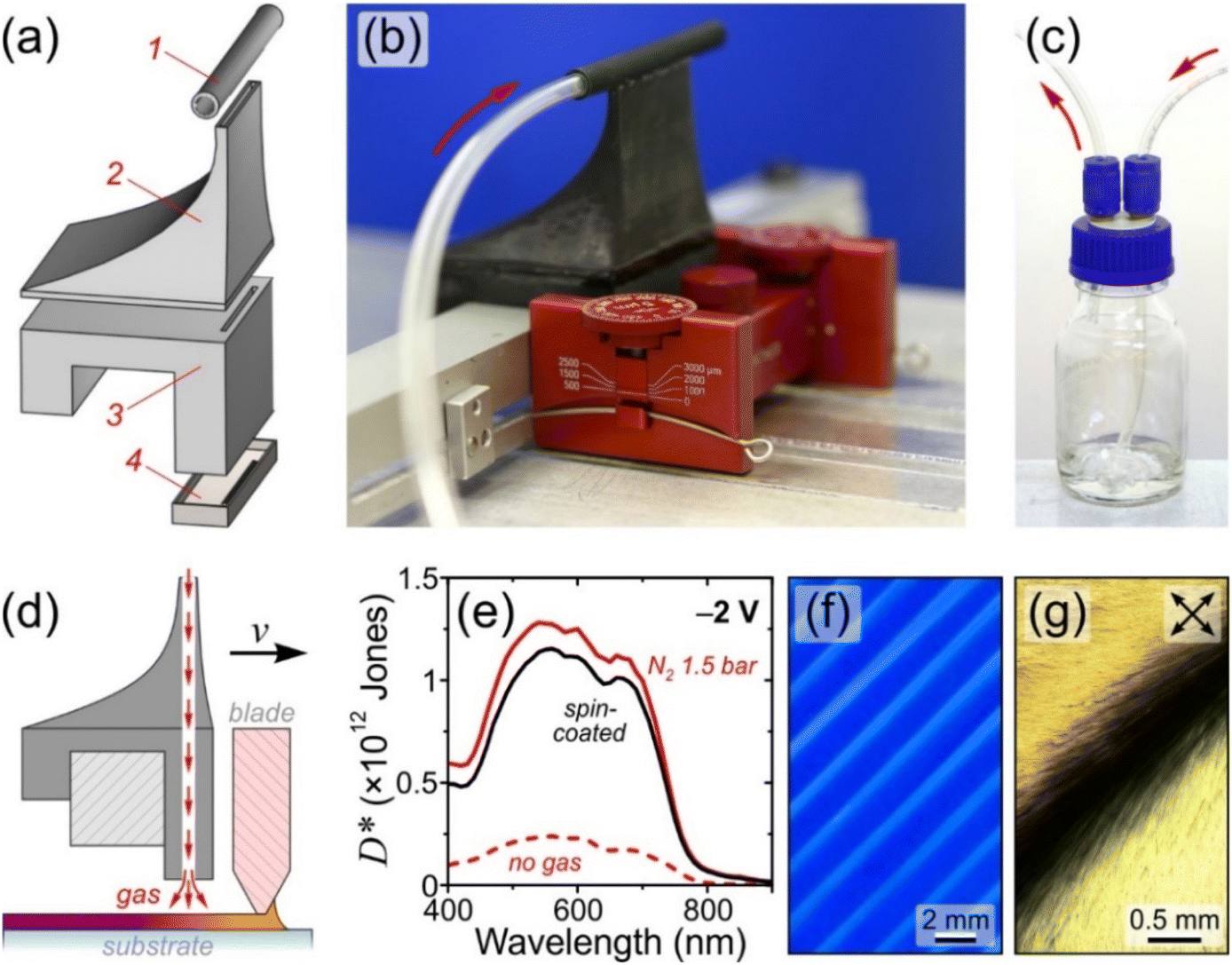 | ||
| Fig. 1 Additional hardware used in gas-assisted blade-coating: (a) schematic illustration of the 3D-printed attachment (1: gas inlet; 2: slot die; 3: slot die and mount, and 4: gas outlet nozzles) and (b and c) photographs of the actual components. (d) Placement in relation to the doctor blade and the substrate. (e) Comparison of specific detectivities D* for OPDs based on spin- and blade-coated (no gas vs. 1.5 bar N2 pressure) P3HT:ITIC active layers. (f) Fluorescence microscopy image of chain conformation line patterns in a polyfluorene film. (g) Cross-polarised micrograph of a chain orientation line pattern in a P3HT:N2200 blend film. | ||
The following sections present the use of drying gas for achieving performance parity between OPDs based on spin- and blade-coated active layers (Fig. 1e), as well as one-step fabrication of chain conformation and orientation patterns (Fig. 1f and g, respectively).
2.2. Upscaling of OPDs
Fig. 2a presents images of selected P3HT:ITIC films blade-coated at increasing N2 drying gas pressures (For completeness, the full set of images is given in Fig. S3a†). Evidently, the reference film coated without drying gas is both highly crystalline and inhomogeneous due to its uncontrolled drying occurring slowly at ambient conditions, additionally resulting in high root-mean-square (RMS) surface roughness, Rq, of 10 ± 4 nm (Fig. S3b†). On the contrary, with the drying gas directed at the substrate through an array of nozzles (inset in Fig. 2b and Fig. S2†), macroscopically homogeneous films with smooth surface topography (Rq = 0.7 ± 0.1 nm; Fig. S3b†) are obtained for gas pressures P ranging from 0.25 to 4 bar. A close inspection of the corresponding film thickness and absorption data in Fig. 2b and c reveal two distinct regimes for the evolution of thin-film characteristics with increasing P.
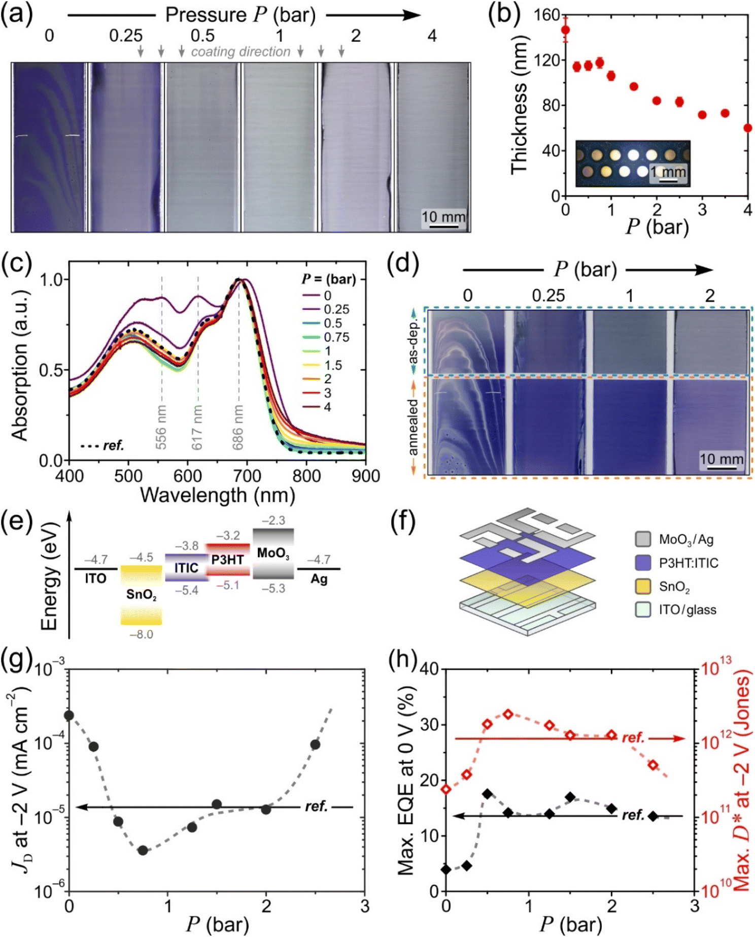 | ||
| Fig. 2 Gas-assisted blade-coating of P3HT:ITIC blend films and their performance as active layers in OPDs. (a) Transmitted-light images of the films blade-coated at increasing N2 gas pressures and the corresponding (b) film thickness and (c) peak-normalised absorption spectra. Coating direction is top-to-bottom in the images. Also shown in (c) is the normalised absorption spectrum of a reference (‘ref.’) spin-coated film. The inset in (b) shows a section of the employed array of gas nozzles. (d) Reflected-light images comparing as-deposited (‘as-dep.’) and thermally annealed films. (e) Energy level diagram for P3HT:ITIC OPDs and (f) the inverted device architecture. (g) Dark-current density JD at −2 V. (h) Maximum values of EQE at 0 V and specific detectivity D* at −2 V. In (g and h) the corresponding values obtained for a reference spin-coated device are indicated by horizontal arrow markers, while the dotted lines are a guide to the eye. | ||
For P = 0.25–0.75 bar, the film thickness remains constant at ∼115 nm. Simultaneously, the peak-normalised absorption spectra in Fig. 2c indicate that crystallinity of the materials is rapidly reduced with increasing P. The increasing A0–0/A0–1 intensity ratio of the ITIC absorption features at, respectively, 686 and 617 nm is characteristic of a progressively lower degree of intermolecular coupling, i.e. a less ordered semicrystalline microstructure.32 Similar observation holds for P3HT, which exhibits an attenuation of its crystalline-phase absorption features at 605 nm (partially overlapping with A0–1 of ITIC) and 556 nm relative to the broad absorption peak centred at ∼500 nm.33 In both cases, the crystallinity reduction saturates rapidly with increasing drying gas pressure, indicating that maximal crystallisation suppression for the blend is achieved for P ≈ 0.5–0.75 bar, which is further evident from the rapid colour change of the films from purple to grey (Fig. 2a). Reassuringly, the normalised absorption spectra recorded for corresponding blade-coated films are identical to that of the reference spin-coated film (dotted line in Fig. 2c).
As an additional confirmation of the relative reduction of blend crystallinity upon gas-assisted drying, Raman spectra were recorded for as-deposited P3HT:ITIC films (Fig. S4†). By virtue of resonant enhancement for excitation at 488 nm (see Materials and Methods), the analysis preferentially probes P3HT, the symmetric C![[double bond, length as m-dash]](https://www.rsc.org/images/entities/char_e001.gif) C stretch mode of which exhibits a characteristic 4 cm−1 shift to higher energies with increasing pressure, saturating for P = 0.5 bar. Such spectral signature is commonly ascribed to increasing molecular disorder24 which herein arises due to a more rapid solvent evaporation and blend vitrification by the drying gas flow.
C stretch mode of which exhibits a characteristic 4 cm−1 shift to higher energies with increasing pressure, saturating for P = 0.5 bar. Such spectral signature is commonly ascribed to increasing molecular disorder24 which herein arises due to a more rapid solvent evaporation and blend vitrification by the drying gas flow.
For P ≥ 1 bar, the degree of crystallinity remains unchanged while the film thickness (Fig. 2b) decreases with pressure at a linear rate of −15 nm bar−1. This may appear counterintuitive given the expectation that high drying gas pressures lead to a transition from the Landau–Levich (decoupled coating and drying) to the evaporative (matching timescales of coating and solvent evaporation) deposition regime.6 However, the data can be rationalised by considering that in the present configuration (Fig. 1d) the non-negligible lateral drying gas flow across the substrate exerts a force on the receding meniscus, thereby resisting the formation of the wet film layer at elevated pressures.
Finally, we confirm that post-deposition annealing at 140 °C can recover the kinetically arrested crystallinity of the blend films fabricated by gas-assisted blade-coating and yield the desired nanoscale phase-separated BHJ microstructure. This moderate annealing temperature in comparison to the glass transition temperature of the P3HT:ITIC blend (estimated to be 75 °C using the Fox equation34) avoids coarse phase-separation35 and is therefore commonly used for polymer:NFA blends.10,27,28,31Fig. 2d compares the images of blade-coated films recorded before and after annealing and shows the reappearance of the characteristic purple colour of crystalline P3HT:ITIC blend for the annealed samples, with identical absorption spectra for the reference spin-coated film and the films blade-coated with P = 0.5–1.5 bar (Fig. S5†). In addition, an exemplary comparison of Raman spectra for films blade-coated using P = 2 bar shows the expected 3 cm−1 shift of the symmetric CC stretching mode of P3HT to lower energies following post-deposition annealing, indicating an increase in molecular order that accompanies crystallisation (Fig. S6†).
 | (1) |
 | (2) |
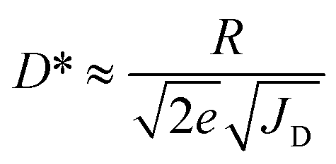
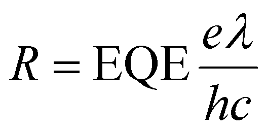
As shown in Fig. 2g, the OPD based on a conventionally (no drying gas) blade-coated active layer exhibits a high JD of 2 × 10⁻⁴ mA cm−2 at 2 V reverse bias. The application of drying gas leads to a rapid suppression of JD by nearly two orders of magnitude, reaching 4 × 10⁻⁶ mA cm−2 for P = 0.75 bar – in fact, marginally surpassing the corresponding value (1 × 10⁻⁵ mA cm−2) measured for the reference spin-coated device and P3HT:ITIC devices reported in the literature.39 At pressures exceeding 1 bar, for which the active layer thickness begins to decrease (Fig. 2b), the expected gradual increase of JD is observed. (For completeness, the full J–V curves are given in Fig. S7.†)
The corresponding maximum EQE (Fig. 2h, left ordinate) of blade-coated devices is similarly enhanced by the use of drying gas, increasing from 3.8% (0 bar) to 13.5–17.5% over the 0.5–2.5 bar range of gas pressures. In comparison, the reference spin-coated device exhibits a maximum EQE of 13.4%. Note that the highest obtained values surpass those reported in the literature for blade-coated P3HT:ITIC devices of comparable architecture (8%)10 while being somewhat lower than those of spin-coated devices using optimised architectures (36%).39 The combined improvements of JD and EQE via the use of in situ drying at P = 0.5–1.5 bar therefore resulted in an order-of-magnitude enhancement of D* up to ∼2 × 10¹² Jones, on par with the spin-coated device (Fig. 2h, right ordinate). To confirm that no further improvements in device performance are possible by harnessing yet more rapid thin-film solidification kinetics, the analysis above was repeated using drying gas saturated in acetonitrile—a non-solvent for both P3HT and ITIC—via a two-terminal vessel (Fig. 1c). As shown in Fig. S7 and S8,† the characteristics of the resulting OPDs match those obtained with using dry N2.
The observations above, summarised in Table 1, can be qualitatively interpreted in terms of the differences in phase-separated BHJ microstructure. Its influence on OPD characteristics has been elegantly studied in the recent work by Go et al.29 for a series of model semiconducting terpolymers, reporting that reduced phase-separation length scales lead to increased responsivity and dark-current suppression. The conventionally blade-coated P3HT:ITIC blend film (P = 0 bar) undergoes very slow drying in comparison to the spin-coated film, resulting in a coarsely phase-separated BHJ microstructure with poor EQE and high JD. The use of mild drying gas pressures (P ≈ 0.5–1.5 bar) accelerates the film formation kinetics for the same solution, matching them with those of spin-coating and yielding comparably vitrified blend microstructures. Thereafter, post-deposition thermal annealing controllably re-introduces both crystallinity and nanoscale phase-separation, for which domain sizes on the order of 10–20 nm are considered optimal for the employed materials.40 The finer scale of phase-separation increases the donor![[thin space (1/6-em)]](https://www.rsc.org/images/entities/char_2009.gif) :acceptor interface area and facilitates exciton dissociation, thereby resulting in improved charge generation efficiency, EQE and spectral responsivity. Simultaneously, the increasingly complex network of charge-transporting pathways leads to a reduction of dark-current.29
:acceptor interface area and facilitates exciton dissociation, thereby resulting in improved charge generation efficiency, EQE and spectral responsivity. Simultaneously, the increasingly complex network of charge-transporting pathways leads to a reduction of dark-current.29
| Deposition | EQEmax at 0 V (%) | J D at −2 V (mA cm−2) | R max at −2 V (mA W−1) |
|
|
|---|---|---|---|---|---|
| 530 nm | 690 nm | ||||
| Blade-coated (no gas) | 3.8 | 1.8 | 2 × 10⁻⁴ | 66 | 0.2 |
| Blade-coated (P = 0.5–1.5 bar) | 15.6 ± 1.6 | 10.5 ± 1.2 | 9 ± 4 × 10⁻⁶ | 88 ± 5 | 1.8 ± 0.4 |
| Spin-coated | 13.4 | 8.8 | 1 × 10⁻⁵ | 77 | 1.2 |

Finally, it is interesting to note that, as shown by the peak-normalised EQE spectra in Fig. S8 in the ESI,† the ITIC band centred at ∼690 nm consistently exhibits a more pronounced enhancement via the use of accelerated drying in comparison to the P3HT band. This indicates the higher tendency of the small-molecular acceptor to form unfavourable solid-state microstructures under slower drying conditions and, therefore, highlights the importance of controlling its solidification kinetics during active layer deposition.
| Deposition | J D (mA cm−2) | R max (mA W−1) |
|
|---|---|---|---|
| Blade-coated (no gas) | 6 × 10⁻⁶ | 240 | 0.5 |
| Blade-coated (P = 1–2 bar) | 2 ± 1 × 10⁻⁶ | 290 ± 9 | 1.4 ± 0.4 |
| Spin-coated | 2 × 10⁻⁶ | 302 | 1.4 |
2.3. 1D chain conformation patterns
While the previous examples employed an array of nozzles to obtain a spatially homogeneous exposure to drying gas, the use of discrete nozzles delivering non-uniform gas flux can enable one-step blade-coating-based fabrication of patterned structures. Here we select poly(9,9-dioctylfluorene) (PFO) as an exemplary light-emitting organic semiconductor for which the differences in drying kinetics can result in dramatic changes in microstructure and optoelectronic properties.42,43 Solution-deposition of PFO films with rapid solvent evaporation forms in-plane isotropic, ‘glassy’ films characterised by disordered, kinetically trapped distribution of chain conformations and deep-blue emission. Delayed solvent evaporation, however, allows a fraction of chain segments to undergo co-crystallisation with the solvent molecules,44,45 forming the uniquely well-defined ‘β-phase’ conformational isomer. By virtue of its extended planar-zigzag conformation, β-phase PFO acts as a ‘self-doped’ system, whereby the presence of a nominally small (typically < 10%) fraction of β-phase chain segments leads to a distinct red-shifted photoluminescence (PL) spectrum, increased PL quantum yield and significant differences in polaron generation and charge transport phenomena.43,46,47 Hence, β-phase PFO is actively used as a model system to study intramolecular-disorder-mediated structure–property relations.46–50 However, obtaining spatial patterns of β-phase for such studies invariably requires inconvenient post-deposition treatments via masked solvent exposure.43One-step formation of alternating β-phase/glassy chain conformation patterns in PFO films by gas-assisted blade-coating is illustrated in Fig. 3. N2 flux is directed at the substrate via an attachment featuring two nozzles spaced 8 mm apart (Fig. S2†). The commonly employed PFO solutions in toluene additionally comprise a small amount of a high-boiling co-solvent (1,2-dichlorobenzene, Tb = 181 °C; see Materials and methods). As shown by the images in Fig. 3a, applying drying gas at P = 0.25 suppresses β-phase formation in film areas directly under the nozzles, yielding essentially pure glassy PFO. This is confirmed by the locally acquired absorption spectrum (Fig. 3b), while the corresponding PL spectrum (Fig. 3c) indicates the presence of only a trace (∼0.1%)43 β-phase fraction. Outside the gas-exposed areas, however, slower drying facilitates β-phase formation, as shown by its well-resolved absorption peak at 435 nm (Fig. 3b) and the characteristic red-shifted PL spectrum (Fig. 3c). Lateral profiling of absorption at 435 nm (Fig. 3d) across the film highlights the smooth variation of β-phase fraction due to the broadened spatial distribution of drying gas flux from nozzles placed at a relatively high distance of 11 mm above the substrate. Importantly, however, the corresponding absorption profile at 385 nm is spatially invariant, indicating that the overall film thickness is not affected by locally applied drying gas at mild pressures.
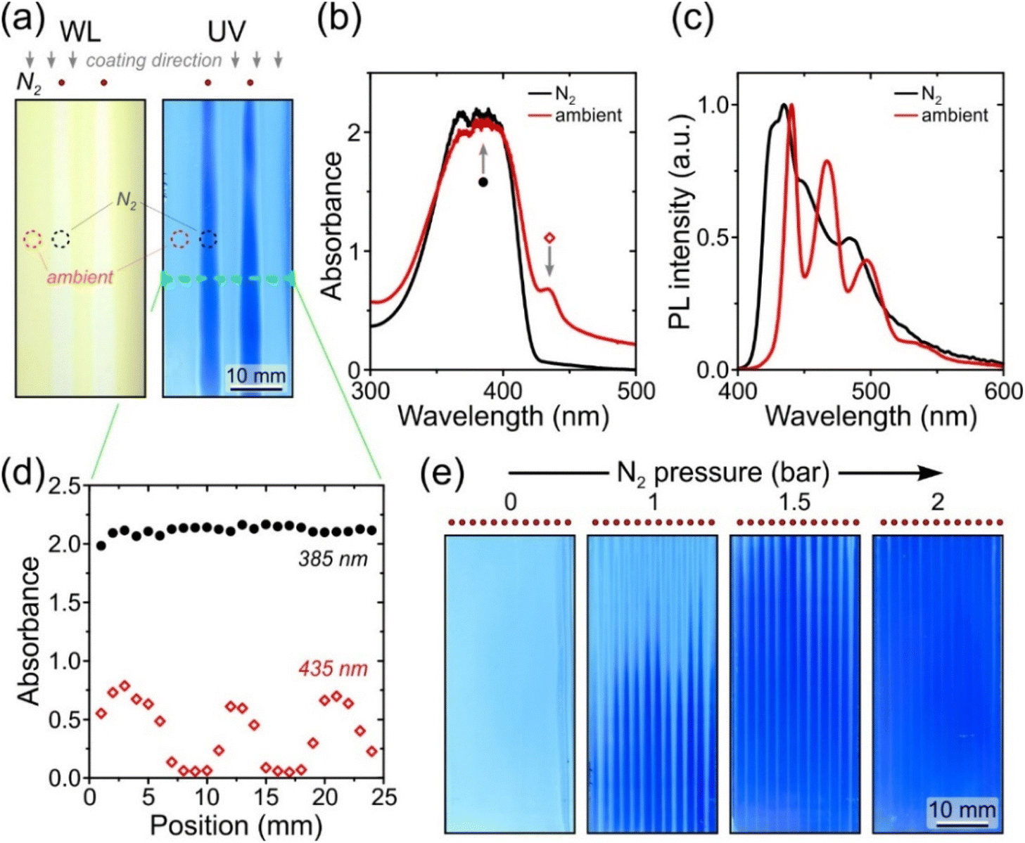 | ||
| Fig. 3 PFO films featuring chain conformation line patterns. (a) Images under white-(WL) and UV-light illumination of a blade-coated PFO film with N2 flux directed via two nozzles (depicted by red circles). (b) Absorption and (c) photoluminescence spectra recorded for film areas directly under, and away from, the nozzles as indicated by the markers in (a). (d) Absorption profiles at 385 nm (predominantly glassy PFO) and 435 nm (β-phase PFO) across the width of the film, as indicated by the dashed line in (a). (e) Fluorescence images of PFO films featuring 1D chain conformation patterns fabricated by directing the N2 flux at increasing pressures through an array of 2 mm-spaced nozzles (depicted by red circles). | ||
The resolution of chain conformation line patterns can be substantially enhanced by placing the nozzles closer, within 3 mm of the substrate, to minimise the effects of lateral spreading of the gas flux exiting the nozzles. As shown by the UV-light images of the films blade-coated with gas-assisted drying through an array of 2 mm-spaced nozzles (Fig. 3e), the fluorescence of the films evolves from homogeneous β-phase (no gas) to β-phase line patterns with progressively diminishing widths for increasing gas pressures. Hence, homogeneous β-phase line patterns can be obtained with widths tuneable from 790 μm (P = 1 bar) to 340 μm (P = 2 bar), as shown by the fluorescence microscopy images in Fig. S10.† Applications of such one-step β-phase patterning in PFO films include the optimisation and prototyping of the recently demonstrated circularly polarised light-emitting diodes based on blends of PFO and chiral small molecules, for which accurate control of β-phase fraction is found to improve device characteristics.50 Elsewhere, with further reduction of line pattern dimensions, the refractive index contrast between glassy and β-phase PFO may be exploited for high-throughput fabrication of photonic structures such as waveguides and refractive index gratings.42
2.4. 2D-oriented donor![[thin space (1/6-em)]](https://www.rsc.org/images/entities/h3_char_2009.gif) :acceptor blend films
:acceptor blend films
Besides governing the degree of crystallinity explored in the preceding examples, in situ gas-assisted drying can also be used to control the directionality of crystal growth for solution-deposited (macro-)molecules to obtain on-demand orientation of organic semiconductor films. As the material system with relevance to both photovoltaic and photodetection applications, we demonstrate this for an all-polymer donor:acceptor blend comprising P3HT and N2200. Directional orientation is enabled by co-deposition with the crystallisable solvent 1,3,5-trichlorobenzene (TCB) which, under particular deposition conditions described in detail in ref. 27, provides a nucleation surface for subsequent epitaxial solidification of organic semiconductors. Hence, key to achieving a high degree of molecular orientation for a given deposition method24–27 is ensuring maximally directional growth of fibrillar TCB crystals in a particular—typically, the coating—direction. The use of accelerated, gas-assisted drying represents an optimal means of obtaining a uniform drying front, which provides a moving gradient in solution supersaturation and, therewith, drives directional crystal growth.
This is illustrated in Fig. 4a by polarised transmitted-light images of a P3HT:N2200 blend film blade-coated with drying gas at P = 2 bar directed at the substrate through an array of nozzles. The dichroic contrast between the images recorded with light polarised parallel and perpendicular to the coating direction indicates both a high degree of chain orientation and its uniformity throughout the film. Polarised absorption profiles across the film confirm the uniformity of optical anisotropy which features maximum dichroic ratios of 5 for both P3HT and N2200 spectral components (Fig. S11†). Reassuringly, the surface roughness of the film (Rq = 15 and 11 nm parallel and perpendicular to the coating direction) is substantially lower than Rq ≈ 30 nm obtained previously for the identical solution and coating parameters but using the less optimal fan-assisted drying.27 This aspect is particularly relevant for the use of these oriented films as active layers in optoelectronic devices.
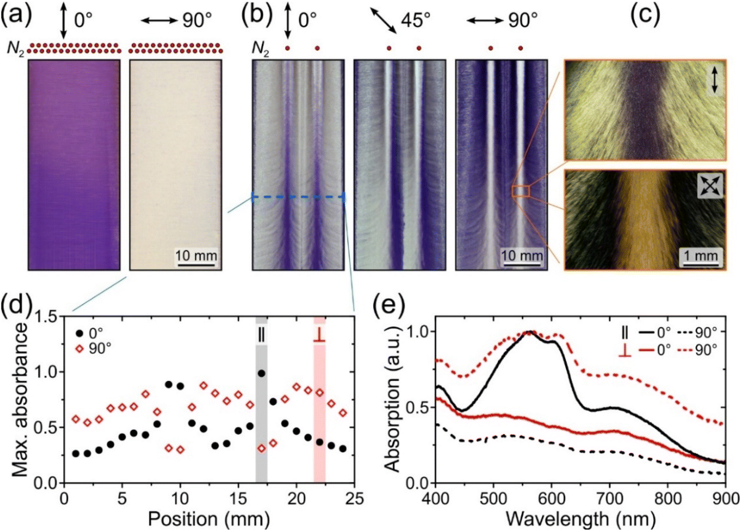 | ||
| Fig. 4 2D-oriented P3HT:N2200 blend films. Polarised transmitted-light images of (a) a reference, uniformly oriented film using N2 flux directed via an array of nozzles and (b) 2D-oriented film using N2 flux directed via two nozzles (depicted by red circles). Polarisation of light with respect to the coating direction (top to bottom in the images) is indicated by ↔. (c) Polarised transmitted-light micrographs centred on the parallel-oriented film area. (d) Profiles of maximum absorbance across the width of the film, as indicated by the dashed line in (b), recorded at 0° and 90° polarisation angles. (e) Polarised absorption spectra for film areas with preferentially parallel (∥, black lines) and perpendicular (⊥, red lines) chain orientation, as indicated by the vertical markers in (d). | ||
An advanced extension of the method involves shaping the drying front to obtain controllable, spatially varying orientation direction. Polarised light images of a P3HT:N2200 film blade-coated using N2 at P = 0.25 bar directed via two nozzles spaced 8 mm apart are shown in Fig. 4b. Image recorded with incident polarisation at 0° with respect to the coating direction exhibits maximal absorption for the film areas directly under the nozzles, indicating local chain orientation parallel to the coating direction enabled by the drying gas. Outside these areas, however, the chain orientation direction progressively changes towards perpendicular to the coating direction, as shown by the 45°- and 90°-polarised images in which film areas exhibiting maximal absorption shift towards substrate edges. Polarised micrographs in Fig. 4c centred on the film area directly under one of the nozzles illustrate this further. The image recorded under 0°-polarised incident light shows a 1 mm-wide stripe exhibiting maximal absorption, outside of which absorption rapidly decreases as the chain orientation veers off axis. Confirming this, the ±45° cross-polarised image shows a reduction of transmitted light intensity outside the central, vertically oriented stripe.
Polarised absorption profiles in Fig. 4d illustrate the presence of well-defined mm-wide film areas where chain orientation is preferentially parallel and perpendicular to the coating direction. Polarised absorption spectra recorded at two representative locations on the sample (Fig. 4e) reveal a somewhat lower optical anisotropy for the perpendicular-oriented film regions, as well as a higher degree of crystallinity evident from the well-resolved vibronic peaks of P3HT.
Qualitatively, the formation of such 2D-oriented microstructure can be understood as follows. Rapid gas-assisted drying of the film areas directly under the nozzles results in chain orientation parallel to the coating direction, while the surrounding areas remain as a thin solution layer. Subsequent crystal growth in the latter areas is directed by the presence of crystal nuclei in parallel-oriented areas, as well as depleted solvent concentration in the immediately adjacent regions, resulting in a preferentially perpendicular-oriented chain orientation. Given this mechanism, the interplay between parallel and perpendicular orientation can be conveniently controlled by solution formulation and deposition conditions. Specifically, maximally sharp transition between parallel- and perpendicular-oriented areas can be achieved by reducing the TCB fraction in solutions and increasing the coating speed (Fig. S12 and S13,† respectively). The applications of one-step blade-coating of 2D-oriented donor:acceptor blend films include the fabrication of complex device arrays within a single substrate, e.g. polarised OPDs with polarisation axes of individual devices oriented in multiple different directions for imaging-based polarimetry analysis.27 Elsewhere, 2D-oriented organic semiconductor films offer a versatile and highly tuneable test-bed for studying anisotropic thermal transport using the emerging high-resolution optical methods.51
3. Conclusions
In summary, we have demonstrated a diverse range of applications of combining in situ gas-assisted drying with the conventional laboratory-scale doctor-blade deposition for organic semiconductor thin-film and device fabrication. Upscaling of active layer deposition without compromising device performance was demonstrated for OPDs based on P3HT:ITIC and PM6:ITIC donor:acceptor blends. For a given solution formulation, the use of mild drying gas pressures of 0.5–2 bar achieved full performance parity with spin-coated devices by matching the drying kinetics. The improvements in responsivity and dark-current suppression yielded a 10-fold improvement in specific detectivity for P3HT:ITIC OPDs relative to conventionally blade-coated devices which was attributed to the formation of a more favourable bulk heterojunction microstructure. In addition, we presented one-step deposition of conformationally structured PFO films featuring β-phase line pattern widths down to 340 μm, as well as 2D-oriented P3HT:N2200 films exhibiting on-demand spatially varying optical anisotropy. Common to these was the use of a 3D-printed attachment, the optimised design of which delivered drying gas flux with a controllable spatial distribution.
Looking ahead, further upscaling of organic semiconductor device fabrication would aim to eliminate the discrete time-consuming post-deposition annealing treatments or the use of degradation-susceptible additives such as 1,8-diiodooctane that are often necessary to optimise crystallinity of donor:acceptor blends. Hence, future work will aim to explore the use of drying gas saturated in selected solvents to direct one-step formation of optimal high-performance microstructures in blade- and slot-die-coated active layers. Elsewhere, the use of solvent-vapour-saturated drying gas to direct favourable, device-architecture-specific vertical phase separation presents a promising avenue for ongoing research.
4. Materials and methods
4.1. Materials
Poly(3-hexylthiophene) (‘P3HT’; Mw ≈ 68000 g mol−1, PDI = 2.4, RR = 95%) was purchased from Rieke Metals. N2200 (CAS no.: 1100243-40-0; Mw ≈ 150000 g mol−1, PDI = 2–3, RR > 99%) and ITIC (CAS no.: 1664293-06-4) were purchased from 1-material. Poly(9,9-dioctylfluorene) (‘PFO’) and 1,3,5-trichlorobenzene (‘TCB’) were purchased from Sigma-Aldrich. PM6 (CAS no.: 1802013-83-7) was purchased from Solarmer. SnO2 dispersion (‘N-31’) was purchased from Avantama. Laboratory-grade solvents purchased from Merck were used throughout. All materials were used as received.
4.2. 3D printing
The additional hardware for gas-assisted blade-coating was fabricated using a SL1 tabletop stereolithographic 3D printer, UV-sensitive thermoset resin (‘tough’ grade) and a CW1 curing/washing accessory (Prusa Research). The design files (FreeCAD; included as part of the ESI†) were converted using the Prusa Slicer software to generate the final model and printing parameters (50 μm lateral resolution and layer height; hollowed-out resin-saving option used).4.3. Thin-film deposition
Blade-coating (Erichsen Coatmaster 510 stage and Zehntner ZUA 2000 applicator) was performed under ambient atmosphere using solutions and substrates preheated to 30 °C and, typically, 50–80 μL of deposited solution, blade gap Δ = 300–500 μm, coating speeds ν = 5–10 mm s−1 and gas nozzles placed 11 mm above the substrate. Unless noted otherwise, dry nitrogen was employed as the gas. P3HT:ITIC and PM6:ITIC films were blade-coated from solutions in chlorobenzene (3.5 wt% and 2.5 wt% respectively, 1:1 wt/wt donor–acceptor ratio; ν = 7 and 5 mm s−1 respectively). The high boiling point of chlorobenzene and near-ambient deposition temperatures ensure slow film-formation kinetics under ambient drying and a gradual transition between Landau–Levich and evaporative deposition regimes for gas-assisted drying. Reference P3HT:ITIC and PM6:ITIC films were spin-coated using the same solutions and substrates pre-heated to 50 °C. PFO films were blade-coated from 3.3 wt% solutions in 4:1 wt/wt toluene:1,2-dichlorobenzene using ν = 5 mm s−1. Uniaxially oriented P3HT:N2200 films were blade-coated from 1.3 wt% solutions in 1:0.22 wt/wt chloroform:TCB. 2D-oriented P3HT:N2200 films were blade-coated from 1.3 wt% solutions in chlorobenzene:TCB (wt/wt solvent ratios ranging from 1:0.5 to 1:1).
4.4. Device fabrication
Glass substrates with pre-structured ITO electrodes (180 nm, 10 Ω □−1; Kintec Co.) were cleaned by sequential sonication in acetone and isopropanol, following which 30 nm-thick SnO2 hole-blocking layers were spin-coated and annealed at 120 °C for 5 min in air. Active layer deposition was performed as described above, followed by annealing for 10 min under N2 atmosphere at 140 °C (P3HT:ITIC) or 100 °C (PM6:ITIC). Devices were completed by thermal evaporation of a 10 nm MoO3 hole transport layer and 100 nm Ag electrode, yielding four 6 × 4 mm2 devices per substrate.4.5. Characterisation
Absorption spectra were recorded using a custom-built setup comprising an AvaLight-DHS-Bal light source and an AvaSpec-ULS3648 spectrometer (no correction for scattering or reflection losses). EQE and spectral responsivity analysis was performed using a 450 W Osram XBO Xenon discharge lamp as a white-light source and an Acton SP-2150i monochromator, while the photocurrent signal was measured with a Stanford Research 830 lock-in amplifier using additional amplification with a Femto DHPCA-100 amplifier. All reported device characteristics correspond to the best-performing, ‘hero’ devices, while the reported average values correspond to 3–4 blade-coated devices with the drying gas pressures in the indicated range. Raman spectroscopy (λex = 488 nm; incident power ≈75 μW) was performed using a WITec Alpha300RA instrument, with the spectra recorded over 60 × 60 μm2 sample areas in scanning mode (0.2 s integration time per spectrum), followed by averaging data from ∼3600 points and subtraction of a polynomial background. Topography analysis was performed with a KLA Tencor D-500 stylus profilometer.Author contributions
AP and GHS conceived and supervised the project. AH and AP undertook preliminary experiments related to gas-assisted blade-coating of directionally oriented blend films. HM and AP performed all other experiments and data analysis. PK and MS advised HM on 3D printing and OPD characterisation. AP wrote the manuscript with contributions from HM and GHS.Conflicts of interest
There are no conflicts to declare.Acknowledgements
AP acknowledges funding by the Federal Ministry of Education and Research (BMBF) and the Baden-Württemberg Ministry of Science as part of the Excellence Strategy of the German Federal and State Governments. The authors are indebted to Prof. Mariano Campoy-Quiles (ICMAB-CSIC) for assistance with Raman spectroscopy and Prof. em. Paul Smith (ETH Zürich) for the many freely shared insights on polymer processing. This work was financially supported by Deutsche Forschungsgemeinschaft (DFG, German Research Foundation) through grant HE 7056/3-1.References
- X. Du, T. Heumueller, W. Gruber, A. Classen, T. Unruh, N. Li and C. J. Brabec, Joule, 2019, 3, 215 CrossRef CAS.
- X. Dai, Y. Deng, C. H. van Brackle and J. Huang, Int. J. Extreme Manuf., 2019, 1, 022004 CrossRef CAS.
- Q. Guo, Q. Guo, Y. Geng, A. Tang, M. Zhang, M. Du, X. Sun and E. Zhou, Mater. Chem. Front., 2021, 5, 3257–3280 RSC.
- J.-L. Wu, L.-H. Lai, Y.-T. Hsiao, K.-W. Tsai, C.-M. Yang, Z.-W. Sun, J.-C. Hsieh and Y.-M. Chang, Adv. Opt. Mater., 2022, 10, 2101723 CrossRef CAS.
- Y. Cui, H. Yao, J. Zhang, K. Xian, T. Zhang, L. Hong, Y. Wang, Y. Xu, K. Ma, C. An, C. He, Z. Wei, F. Gao and J. Hou, Adv. Mater., 2020, 32, 1908205 CrossRef CAS PubMed.
- X. Gu, L. Shaw, K. Gu, M. F. Toney and Z. Bao, Nat. Commun., 2018, 9, 534 CrossRef PubMed.
- L. Merklein, D. Daume, F. Braig, S. Schlisske, T. Rödlmeier, M. Mink, D. Kourkoulos, B. Ulber, M. Di Biase, K. Meerholz, G. Hernandez-Sosa, U. Lemmer, H. M. Sauer, E. Dörsam, P. Scharfer and W. Schabel, Colloids Interfaces, 2019, 3, 32 CrossRef CAS.
- N. Strobel, M. Seiberlich, R. Eckstein, U. Lemmer and G. Hernandez-Sosa, Flexible Printed Electron., 2019, 4, 043001 CrossRef CAS.
- A. S. Gertsen, M. Fernández Castro, R. R. Søndergaard and J. W. Andreasen, Flexible Printed Electron., 2020, 5, 014004 CrossRef CAS.
- E. Pascual-San-José, X. Rodríguez-Martínez, R. Adel-Abdelaleim, M. Stella, E. Martínez-Ferrero and M. Campoy-Quiles, J. Mater. Chem. A, 2019, 7, 20369–20382 RSC.
- J. B. Whitaker, D. H. Kim, B. W. Larson, F. Zhang, J. J. Berry, M. F. A. M. van Hest and K. Zhu, Sustainable Energy Fuels, 2018, 2, 2442–2449 RSC.
- H. Zhao, B. Lin, J. Xue, H. B. Naveed, C. Zhao, X. Zhou, K. Zhou, H. Wu, Y. Cai, D. Yun, Z. Tang and W. Ma, Adv. Mater., 2022, 2105114 CrossRef CAS PubMed.
- C. M. Stafford, K. E. Roskov, T. H. Epps III and M. J. Fasolka, Rev. Sci. Instrum., 2006, 77, 023908 CrossRef.
- L. J. Richter, D. M. DeLongchamp and A. Amassian, Chem. Rev., 2017, 117, 6332–6366 CrossRef CAS PubMed.
- K. Zhao, H. Hu, E. Spada, L. K. Jagadamma, B. Yan, M. Abdelsamie, Y. Yan, L. Yu, R. Munir, R. Li, G. O. Ngongang Ndjawa and A. Amassian, J. Mater. Chem. A, 2016, 4, 16036–16046 RSC.
- G. Ji, W. Zhao, J. Wei, L. Yan, Y. Han, Q. Luo, S. Yang, J. Hou and C.-Q. Ma, J. Mater. Chem. A, 2019, 7, 212–220 RSC.
- S. Lee, D. Jeong, C. Kim, C. Lee, H. Kang, H. Y. Woo and B. J. Kim, ACS Nano, 2020, 14, 14493–14527 CrossRef PubMed.
- C. Sprau, A. M. Cruz, L. Bautista, L. Molina, M. Wagner, C. L. Chochos, M. Della Pirriera and A. Colsmann, Adv. Energy Sustainability Res., 2021, 2, 2100043 CrossRef.
- T. R. Andersen, F. Zhao, Y. Li, M. Dickinson and H. Chen, Sol. RRL, 2020, 4, 2000246 CrossRef CAS.
- I. Pelse, A. L. Jones, L. J. Richter and J. R. Reynolds, Chem. Mater., 2021, 33, 657–667 CrossRef CAS.
- D. Burkitt, R. Swartwout, J. McGettrick, P. Greenwood, D. Beynon, R. Brenes, V. Bulovic and T. Watson, RSC Adv., 2019, 9, 37415–37423 RSC.
- S. Ternes, T. Börnhorst, J. A. Schwenzer, I. M. Hossain, T. Abzieher, W. Mehlmann, U. Lemmer, P. Scharfer, W. Schabel, B. S. Richards and U. W. Paetzold, Adv. Energy Mater., 2019, 9, 1901581 CrossRef CAS.
- J. Ding, Q. Han, Q.-Q. Ge, D.-J. Xue, J.-Y. Ma, B.-Y. Zhao, Y.-X. Chen, J. Liu, D. B. Mitzi and J.-S. Hu, Joule, 2019, 3, 402–416 CrossRef CAS.
- A. Perevedentsev and M. Campoy-Quiles, Nat. Commun., 2020, 11, 3610 CrossRef PubMed.
- B. Dörling, V. Vohra, T. T. Dao, M. Garriga, H. Murata and M. Campoy-Quiles, J. Mater. Chem. C, 2014, 2, 3303–3310 RSC.
- T. Rödlmeier, T. Marszalek, M. Hel, S. Beck, C. Müller, R. Eckstein, A. J. Morfa, R. Lovrincic, A. Pucci, U. Lemmer, J. Zaumseil, W. Pisula and G. Hernandez-Sosa, Chem. Mater., 2017, 29, 10150–10158 CrossRef.
- A. Perevedentsev, H. Mejri, L. A. Ruiz-Preciado, T. Marszalek, U. Lemmer, P. W. M. Blom and G. Hernandez-Sosa, Adv. Opt. Mater., 2022, 10, 2102397 CrossRef CAS.
- N. Strobel, N. Droseros, W. Köntges, M. Seiberlich, M. Pietsch, S. Schlisske, F. Lindheimer, R. R. Schröder, U. Lemmer, M. Pfannmöller, N. Banerji and G. Hernandez-Sosa, Adv. Mater., 2020, 32, 1908258 CrossRef CAS PubMed.
- E. Go, H. Jin, S. Yoon, S. Park, S. H. Park, H. Yu and H. J. Son, ACS Photonics, 2022, 9, 2056–2065 CrossRef CAS.
- V. Belova, A. Perevedentsev, J. Gorenflot, C. S. P. de Castro, M. Casademont-Viñas, S. H. K. Paleti, S. Karuthedath, D. Baran, F. Laquai and M. Campoy-Quiles, Sol. RRL, 2021, 2100822 Search PubMed.
- Y. Qin, M. A. Uddin, Y. Chen, B. Jang, K. Zhao, Z. Zheng, R. Yu, T. J. Shin, H. Y. Woo and J. Hou, Adv. Mater., 2016, 28, 9416–9422 CrossRef CAS PubMed.
- L. Ciammaruchi, O. Zapata-Arteaga, E. Gutierrez-Fernandez, J. Martin and M. Campoy-Quiles, Mater. Adv., 2020, 1, 2846–2861 RSC.
- N. Seidler, G. M. Lazzerini, G. L. Destri, G. Marletta and F. Cacialli, J. Mater. Chem. C, 2013, 1, 7748–7757 RSC.
- T. G. Fox, Bull. Am. Phys. Soc., 1956, 1, 123–125 CAS.
- Z. Wang, K. Gao, Y. Kan, M. Zhang, C. Qiu, L. Zhu, Z. Zhao, X. Peng, W. Feng, Z. Qian, X. Gu, A. K. Y. Jen, B. Z. Tang, Y. Cao, Y. Zhang and F. Liu, Nat. Commun., 2021, 12, 332 CrossRef CAS PubMed.
- C. M. Lochner, Y. Khan, A. Pierre and A. C. Arias, Nat. Commun., 2014, 5, 5745 CrossRef CAS PubMed.
- Y. Guo, Y. Li, Q. Zhang and H. Wang, J. Mater. Chem. C, 2017, 5, 1436–1442 RSC.
- G. Simone, M. J. Dyson, C. H. L. Weijtens, S. C. J. Meskers, R. Coehoorn, R. A. J. Janssen and G. H. Gelinck, Adv. Opt. Mater., 2020, 8, 1901568 CrossRef CAS.
- G. Yang, Z. Wang, Y. Duan, D. Zhao and J. Yu, Nanoscale Res. Lett., 2019, 14, 201 CrossRef PubMed.
- F. Zhao, C. Wang and X. Zhan, Adv. Energy Mater., 2018, 8, 1703147 CrossRef.
- Y. Wang, Q. Fan, X. Guo, W. Li, B. Guo, W. Su, X. Ou and M. Zhang, J. Mater. Chem. A, 2017, 5, 22180–22185 RSC.
- A. Perevedentsev, Y. Sonnefraud, C. R. Belton, S. Sharma, A. E. G. Cass, S. A. Maier, J.-S. Kim, P. N. Stavrinou and D. D. C. Bradley, Nat. Commun., 2015, 6, 5977 CrossRef CAS PubMed.
- A. Perevedentsev, N. Chander, J.-S. Kim and D. D. C. Bradley, J. Polym. Sci., Part B: Polym. Phys., 2016, 54, 1995–2006 CrossRef CAS PubMed.
- A. Perevedentsev, P. N. Stavrinou, D. D. C. Bradley and P. Smith, J. Polym. Sci., Part B: Polym. Phys., 2015, 53, 1481–1491 CrossRef CAS PubMed.
- A. Perevedentsev, P. N. Stavrinou, P. Smith and D. D. C. Bradley, J. Polym. Sci., Part B: Polym. Phys., 2015, 53, 1492–1506 CrossRef CAS PubMed.
- N. J. Cheetham, M. Ortiz, A. Perevedentsev, L. I. Dion-Bertrand, G. M. Greetham, I. V. Sazanovich, M. Towrie, A. W. Parker, J. Nelson, C. Silva, D. D. C. Bradley, S. C. Hayes and P. N. Stavrinou, Chem. Mater., 2019, 31, 6787–6797 CrossRef CAS.
- X. Shi, V. Nádaždy, A. Perevedentsev, J. M. Frost, X. Wang, E. Von Hauff, R. C. I. MacKenzie and J. Nelson, Phys. Rev. X, 2019, 9, 021038 CAS.
- A. Perevedentsev, S. Aksel, K. Feldman, P. Smith, P. N. Stavrinou and D. D. C. Bradley, J. Polym. Sci., Part B: Polym. Phys., 2015, 53, 22–38 CrossRef CAS.
- B. Laidlaw, J. Eng, J. Wade, X. Shi, F. Salerno, M. J. Fuchter and T. J. Penfold, Chem. Commun., 2021, 57, 9914–9917 RSC.
- L. Wan, X. Shi, J. Wade, A. J. Campbell and M. J. Fuchter, Adv. Opt. Mater., 2021, 9, 2100066 CrossRef CAS.
- L. A. Pérez, K. Xu, M. R. Wagner, B. Dörling, A. Perevedentsev, A. R. Goñi, M. Campoy-Quiles, M. I. Alonso and J. S. Reparaz, Rev. Sci. Instrum., 2022, 93, 034902 CrossRef PubMed.
Footnote |
| † Electronic supplementary information (ESI) available. See DOI: https://doi.org/10.1039/d2nr05947a |
| This journal is © The Royal Society of Chemistry 2022 |